Download to read offline


![International Research Journal of Engineering and Technology (IRJET) e-ISSN: 2395-0056
Volume: 04 Issue: 08 | Aug -2017 www.irjet.net p-ISSN: 2395-0072
RESULT REFERENCES
[1]. Farshad Moradi, Dag T. Wisland, Ali Peiravi , Hamid
Mahmoodi (2008)1-Bit Sub Threshold Full Adders in
65nm CMOS Technology International conference on
Microelectronics 1- 4244-2370-5/08/$20.00 ©2008
IEEE
[2]. S. Wariya, Himanshu Pandey, R. K. Nagaria and
S. Tiwari ,(2010)Ultra low voltage high speed 1bit adder,
IEEE Transactions Very Large Scale Integeration.
[3]. Praveer Saxena, Dinesh Chandra, Sampath Kumar
V(2011) Design of 1-Bit Full Adder for Low Power
Applications IJAEST,Vol No. 10 Issue No.1,019-025
[4]. Shamima Khatoon (2012)A novel design for highly
compact low power area efficient 1-bit Full Adders
,IJAET
[5]. Keivan Navi and Omid Kavehei(2008)Low- Power and
High-Performance 1-Bit CMOS Full- Adder Cell
JOURNAL OF COMPUTERS, VOL. 3, NO. 2, FEBRUARY
2008
AUTHOR’S BIOGRAPHY
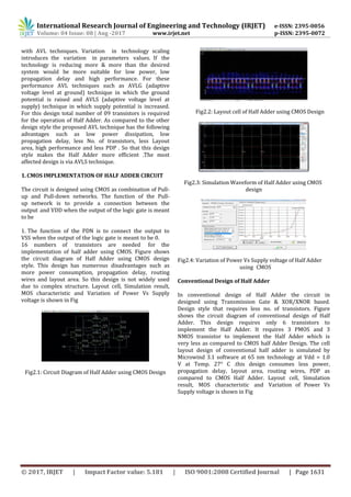
CONCLUSIONS
From the above result we can see that the simulation
result of this half adder using Adaptive Voltage Level
technique shows that the power consumption is much
reduced as compared to other techniques .Propagation
delay, layout area, PDP also reduced as compared to
other technique. It also requires less routed wires as
compared to CMOS design. Various parameters have
been calculated by using Micro wind 3.1 at 65 nm
technology. Design of Half Adder using AVLS technique is
more efficient in speed, layout area, power
consumption, routed wires and propagation delay as
compared to other technique. All the circuits operate at
supply voltage of 1.2 V and temp. of 27°C.By using AVL
technique size of circuit is also reduced. The application of
AVL technique is used to reduce the power dissipation of
digital circuits. By using AVL technique power can be
saved up to 60 %.
Mateshwar Singh received his B. Tech
Degree in Electronics and Communication
Engineering from H.C.S.T Farah Mathura
and he is pursuing M.Tech in VLSI Design
from NIET Greater Noida.
Surya Deo Choudhary has received his
Ph.D. degree in Electronics & Communication
Engineering from B.R. Ambedkar Bihar
University in 2015. He has received his
M.Tech. degree from BIT Sindri, Dhanbad in
2011 and B.Tech. in 2008.
He is working as an Assistant Professor in
Department of Electronics and
Communication Engineering at Noida
Institute of Engineering and Technology,
Greater Noida. He has published many
International and National Journals. His area
of research is Antenna & Microwave,
Passive Filters.
Ashutosh Kumar Singh has 8 years of
Teaching Experience and currently working
as an Assistant Professor in Department of
Electronics and Communication Engineering
at Noida Institute of Engineering and
Technology, Greater Noida.
He has completed his Masters in VLSI Design,
2013 and B.Tech in Electronics and
communication Engineering, 2009 from
Uttar Pradesh Technical University,
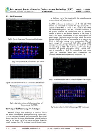
S.
No. Parameters C-CMOS Conventional
AVL
G AVLS
1. Power
Consumption
(µw)
7.348 0.502 0.383 0.321
2. Routed Wires 50 14 35 30
3. Compiled Cells 16 / 16 6 / 6 9 / 9 9 / 9
4.
Layout Area
2
(µm ) 232 96 136 128
5.
Propagation
Delay (ns) 0.70 0.67 0.65 0.54
6. PDP (fj) 5.1436 0.33634 0.2485
0.173
34
7.
No. of N-MOS
and P- MOS
transistors
8, 8 3, 3 5,4 4 ,5
© 2017, IRJET | Impact Factor value: 5.181 | ISO 9001:2008 Certified Journal | Page 1634](https://image.slidesharecdn.com/irjet-v4i8292-170922104145/85/Design-Simulation-of-Half-Adder-Circuit-using-AVL-Technique-Based-on-CMOS-Technology-5-320.jpg)


The document describes the design and simulation of a half adder circuit using an adaptive voltage level (AVL) technique based on 65nm CMOS technology. It summarizes that the AVL technique can significantly reduce the power consumption of half adder circuits compared to conventional CMOS and transmission gate-based designs. Specifically, simulation results show that an AVL design using an adaptive voltage level at the supply achieves the lowest power consumption of 0.321μW, fastest propagation delay of 0.54ns, and smallest power-delay product of 0.1734fJ compared to other techniques. The AVL supply technique provides the most efficient half adder design in terms of speed, area, power, and routing.