Download to read offline
![International Research Journal of Engineering and Technology (IRJET) e-ISSN: 2395-0056
Volume: 07 Issue: 03 | Mar 2020 www.irjet.net p-ISSN: 2395-0072
© 2020, IRJET | Impact Factor value: 7.34 | ISO 9001:2008 Certified Journal | Page 2567
Low Power Design for Fast Full Adder
R.Deebigai1, P.Krishnakumar2
1Student, Dept. of Electronics and Communication Engineering, Tamil Nadu, India
2Assistant Professor, Dept. of Electronics and Communication Engineering, Tamil Nadu, India
---------------------------------------------------------------------***---------------------------------------------------------------------
Abstract - Inthe era of digitalization, the unbendingdrive
in the semiconductor industry for smaller, faster, cheaper
integrated circuits has brought the industry to the 45nm
technology. In this paper, the design for full adder which is
highly optimized in terms of power consumption and area,
featuring hybrid CMOS design style. To examine the
performance of the proposed system, Tanner EDA
simulations based on 45nm Complementary Metal-Oxide
Semiconductor (CMOS) process technology used. This
technology significantly reduces the power of the circuit
during idle periods such that leakage power is no longer
factor. This, in turn, helps extend battery life in battery-
operated portable devices and has major advancement over
previous. This paper explores the fast full addercircuitusing
XOR/XNOR gates and optimizes the PDP (Power Delay
Product). By reducing area and power consumption, this
circuit has high speed, optimized PDP. The proposed full
adder has the good driving capability, power consumption
and so on. The proposed architecture results are compared
to area, power and delay of the existing.
Key Words: 45nm, Area, Full Adder, Hybrid-CMOS
design style, PDP, XOR/XNOR.
1. INTRODUCTION
In the past decades, the major challenge for the VLSI
designer was area, performance, cost and power
consumption. In recent years,thetrendforCMOStechnology
has improved and need to integrate more functions in a
given silicon area. According to Moore’s law, number of
transistor in a chip doubles every two year at the same time
the cost of the computer is halved. In detail, the speed and
capability of computer increases for every two yearandcost
will reduced. As increase in no. of transistor in a chip, power
will be increased and processing time of each transistoralso
increases. Thus, there will be loss in performance, to
compensate for the performanceloss useofeitherparallel or
pipelined implementations [2]. A parallel implementation
just doubles hardware thus pipelining is for low power
solutions. Many full adder circuits were designed using
various logic styles; each of them has its own merits and
demerits. A full adder is a basic circuit that does all
computations from counting to multiplication to filtering. A
fast and accurate operation of a digital system is greatly
influenced by the performance of the resident adders.These
in turn, form the core of any system and thereby influence
the overall performance of the entire system.
1.1 65nm to 45nm CMOS TECHNOLOGY
CMOS manufacturing for the design of processortoshrink in
the size of the transistors, which means more can befitted in
the same space, with a number of implications. At the
starting stage, today’s processor design cannot be
implemented as it is unfeasiblymassive.Powerconsumption
is also another issue.Smaller transistorconsumeslesspower
but practically there will more transistors than with a larger
process technology. Due to low power consumption,
transistor won’t get hot thus at higher frequency the
processor performs without burning or overloading the
mother-board power supply [11]. The production cost will
become cheaper to make. Thus, a 45nm processor takes up
half the area of a 65nm one with the same design. It has 23%
gate delay reduction compared to 65nm at the Ioff and 10%
lower VDD. It has less power leakage and greater power
efficiency [12].
1.2 LOW POWER DESIGN
As VLSI technology advances, the complexity and speed of
the circuit increases, resulting in high power dissipation.
Power dissipation has become important constraint in
semiconductor industry. The two major power dissipations
are
1. Dynamic power dissipation, which is caused by two
factors:
Charging and discharging of the capacitor
Short-circuit current, when both pMOS and nMOS
are partially ON.
2. Static power dissipation, when the circuit remains in the
idle state over a period of time, then there will leakage of
current. These leakage current are caused by factors:
Sub-threshold leakage
Gate leakage
Diode leakage
Gate oxide tunneling
Increased usage of the battery-operated portable
devices like, cellular phones, personal digital assistants
(PDAs) and tablets demand VLSIandULSI(Ultra-Large-Scale
Integration) designs, with an improved power-delay
characteristic [3]. For all the aforementioned devices, most
or all of them switching activity may be stopped when it
arrive in idle i.e., sleep mode. Consequently, in addition to](https://image.slidesharecdn.com/irjet-v7i3510-201221025331/85/IRJET-Low-Power-Design-for-Fast-Full-Adder-1-320.jpg)
![International Research Journal of Engineering and Technology (IRJET) e-ISSN: 2395-0056
Volume: 07 Issue: 03 | Mar 2020 www.irjet.net p-ISSN: 2395-0072
© 2020, IRJET | Impact Factor value: 7.34 | ISO 9001:2008 Certified Journal | Page 2567
Low Power Design for Fast Full Adder
R.Deebigai1, P.Krishnakumar2
1Student, Dept. of Electronics and Communication Engineering, Tamil Nadu, India
2Assistant Professor, Dept. of Electronics and Communication Engineering, Tamil Nadu, India
---------------------------------------------------------------------***---------------------------------------------------------------------
Abstract - Inthe era of digitalization, the unbendingdrive
in the semiconductor industry for smaller, faster, cheaper
integrated circuits has brought the industry to the 45nm
technology. In this paper, the design for full adder which is
highly optimized in terms of power consumption and area,
featuring hybrid CMOS design style. To examine the
performance of the proposed system, Tanner EDA
simulations based on 45nm Complementary Metal-Oxide
Semiconductor (CMOS) process technology used. This
technology significantly reduces the power of the circuit
during idle periods such that leakage power is no longer
factor. This, in turn, helps extend battery life in battery-
operated portable devices and has major advancement over
previous. This paper explores the fast full addercircuitusing
XOR/XNOR gates and optimizes the PDP (Power Delay
Product). By reducing area and power consumption, this
circuit has high speed, optimized PDP. The proposed full
adder has the good driving capability, power consumption
and so on. The proposed architecture results are compared
to area, power and delay of the existing.
Key Words: 45nm, Area, Full Adder, Hybrid-CMOS
design style, PDP, XOR/XNOR.
1. INTRODUCTION
In the past decades, the major challenge for the VLSI
designer was area, performance, cost and power
consumption. In recent years,thetrendforCMOStechnology
has improved and need to integrate more functions in a
given silicon area. According to Moore’s law, number of
transistor in a chip doubles every two year at the same time
the cost of the computer is halved. In detail, the speed and
capability of computer increases for every two yearandcost
will reduced. As increase in no. of transistor in a chip, power
will be increased and processing time of each transistoralso
increases. Thus, there will be loss in performance, to
compensate for the performanceloss useofeitherparallel or
pipelined implementations [2]. A parallel implementation
just doubles hardware thus pipelining is for low power
solutions. Many full adder circuits were designed using
various logic styles; each of them has its own merits and
demerits. A full adder is a basic circuit that does all
computations from counting to multiplication to filtering. A
fast and accurate operation of a digital system is greatly
influenced by the performance of the resident adders.These
in turn, form the core of any system and thereby influence
the overall performance of the entire system.
1.1 65nm to 45nm CMOS TECHNOLOGY
CMOS manufacturing for the design of processortoshrink in
the size of the transistors, which means more can befitted in
the same space, with a number of implications. At the
starting stage, today’s processor design cannot be
implemented as it is unfeasiblymassive.Powerconsumption
is also another issue.Smaller transistorconsumeslesspower
but practically there will more transistors than with a larger
process technology. Due to low power consumption,
transistor won’t get hot thus at higher frequency the
processor performs without burning or overloading the
mother-board power supply [11]. The production cost will
become cheaper to make. Thus, a 45nm processor takes up
half the area of a 65nm one with the same design. It has 23%
gate delay reduction compared to 65nm at the Ioff and 10%
lower VDD. It has less power leakage and greater power
efficiency [12].
1.2 LOW POWER DESIGN
As VLSI technology advances, the complexity and speed of
the circuit increases, resulting in high power dissipation.
Power dissipation has become important constraint in
semiconductor industry. The two major power dissipations
are
1. Dynamic power dissipation, which is caused by two
factors:
Charging and discharging of the capacitor
Short-circuit current, when both pMOS and nMOS
are partially ON.
2. Static power dissipation, when the circuit remains in the
idle state over a period of time, then there will leakage of
current. These leakage current are caused by factors:
Sub-threshold leakage
Gate leakage
Diode leakage
Gate oxide tunneling
Increased usage of the battery-operated portable
devices like, cellular phones, personal digital assistants
(PDAs) and tablets demand VLSIandULSI(Ultra-Large-Scale
Integration) designs, with an improved power-delay
characteristic [3]. For all the aforementioned devices, most
or all of them switching activity may be stopped when it
arrive in idle i.e., sleep mode. Consequently, in addition to](https://image.slidesharecdn.com/irjet-v7i3510-201221025331/75/IRJET-Low-Power-Design-for-Fast-Full-Adder-1-2048.jpg)
![International Research Journal of Engineering and Technology (IRJET) e-ISSN: 2395-0056
Volume: 07 Issue: 03 | Mar 2020 www.irjet.net p-ISSN: 2395-0072
© 2020, IRJET | Impact Factor value: 7.34 | ISO 9001:2008 Certified Journal | Page 2568
dynamic power, static power consumptionlimitsthebattery
life while idle. Dynamic power dissipation dominates chip
when active and it can written as
Pdynamic=αCVDD
2f
Thus, by reducing the activity factor (α), switching
capacitance (C), power-supply (VDD) and operating
frequency (f) dynamic power can be reduced. As mentioned
before static power appears when the deviceintheidlestate
and it can be written as
Pstatic=IstaticVDD
Static power dissipation is the product of total leakage
current (Istatic) and the supply voltage (VDD), thus by
minimizing the Istatic static power is reduced.
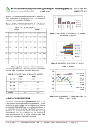
2. DESIGN APPORACH
Hybrid FAs are designed using more than one logic style and
these adders are made of three modules, XOR/XNOR gate to
generate So and 2 to 1 multiplexer to generate Co[3] in fig-1.
Optimum design of XOR/XNOR is required, as it consumes
more power, there will be performance loss. Based on the
output voltage level, circuits can be divided into full swing
and non-full swing categories [1].
Fig-1: MODULE OF FULL ADDER
2.1 GATE LOGIC STYLE
Fig-2: FULL SWING XOR/XNOR USING DPL
Fig-2, the full swing XOR/XNOR gatecircuits[6]basedon the
Double Pass-transistorLogic (DPL) style.Themodel contains
8 transistors but the problem associated with this structure
is that it has NOT gate on the critical path which consumes
more power. The increasing size of the transistor in NOT
gate will lower the critical path delay but it causes large
output capacitance.
Fig-3: FULL SWING XOR/XNOR USING PASS-TRANSISTOR
Fig-3 [7] is based on the Pass-transistor logic style. This
model consists of 6 transistors. The problemassociated with
this structure is that the XOR circuit has lowerdelaythanthe
XNOR circuit since the critical path of the XNOR circuit has
pMOS and NOT gate which is slower than nMOS transistor.
Fig-4: XOR/XNOR CIRCUIT USING CPL
Fig-4 [6], the circuit is based on Complementary Pass
transistor Logic (CPL) this increase the speed and overcome
the above drawback but problem associated with this is that
is cross-coupled (feedback)which increase the delay of the
circuit, another drawback is that existence of the two NOT
gates on the circuit.
2.2 XOR/XNOR CIRCUITS
Fig-5(a): NON-FULL SWING XOR/XNOR
The non-full swing XOR/XNOR fig-5(a)isefficientinterms of
the power and delay, but this structure has one drawback
that at one logical value there is an output voltage drop
problem. To overcome, they introduce the NOT gates. Thus](https://image.slidesharecdn.com/irjet-v7i3510-201221025331/85/IRJET-Low-Power-Design-for-Fast-Full-Adder-2-320.jpg)
![International Research Journal of Engineering and Technology (IRJET) e-ISSN: 2395-0056
Volume: 07 Issue: 03 | Mar 2020 www.irjet.net p-ISSN: 2395-0072
© 2020, IRJET | Impact Factor value: 7.34 | ISO 9001:2008 Certified Journal | Page 2569
for all possible input combinations, the output of the
structure is full swing in fig-5(b) [1].
Fig-5(b): FULL SWING XOR/XNOR GATE
2.3 SIMULTANEOUS XOR/XNOR
Fig-6: SIMULTANEOUS XOR/XNOR CIRCUIT
This structure made of 12 transistors shown in the fig-6. The
model is obtained by combining two fig-5(b) [1].This model
doesn’t have any NOT gate on the critical path of the circuit
and there will be very small output capacitance, thus the
performance of the system is high i.e., processing speed is
high and it consumes less power. Due to this, it has the good
driving capability.
3. PROPOSED FULL ADDER
The proposed full adder is implemented based on the Swith
hybrid logic style, in 45nmCMOSprocess technology.For the
module I, implementation of 6newhybridfull addersand for
module 3,2to1 MUX been used to generate Co. The most
common implementationof MUXis usingTransmissiongates
(TG) in fig-7.But the problem with that, it cannot provide a
good driving capability to drive cascaded stages [3].Thus
introducing output buffer which overcome that problem.
Fig-7: 2-1MUX USING TG LOGIC STYLE
The new hybrid full adder is designed with 20T, 17T, 26T,
22T, 19T in fig-8. The first hybrid FA is designed using 20T
along with MUX.
Fig-8: PROPOSED 6 NEW HYBRID FULL ADDER CIRCUITS
The structure doesn’t have NOT gate on the critical path of
the circuit, thus it has high speed and low power dissipation.
But when this structure is used in cascaded stages, output
driving capability will reduce. To, overcome the
implementation of 17T in fig-8 (b). In this structure, NOT
gate is used. The usage of NOT gate slightly improves the
driving capability. The power consumption is almost the
same as the 20T model as using NOT gate consumes power.
For good driving capability, using a buffer is important. As
VLSI technologyimproves its drivingcapabilitydegrades due
to the presence of the parasitic capacitance and resistance,
the output buffers improve the situation [1]. Fig-8(c) HFA-
26T designed with 26 transistors, MUX, bufferandNOTgate.
The output nodes are driven by input which reduces the
resistance but the delay and power consumption will be
more when compared with the HFA-20T and HFA-17T. The
new buffer is introduced at the input nodes. Fig-8(d)
implements HFA-NB-26T buffer at the input that doesn’t
drive the output node. Using of NOT gate will improve the
driving capability. The delay will be low when compared
with the HFA-26T. The outputs are produced bySum,Co,and
XOR/XNOR.
The output So can also be produced by Co. Goel et al. :[3]
Co = · H´+ Cin · H
This will produce So output. Thus XOR/XNOR will not drive
So, through data select lines of MUX it produces the output.
The above mentioned is implemented in HFA-19T and HFA-
22T in Fig-8(e) and 8(f). The capacitance of the circuit is](https://image.slidesharecdn.com/irjet-v7i3510-201221025331/85/IRJET-Low-Power-Design-for-Fast-Full-Adder-3-320.jpg)
![International Research Journal of Engineering and Technology (IRJET) e-ISSN: 2395-0056
Volume: 07 Issue: 03 | Mar 2020 www.irjet.net p-ISSN: 2395-0072
© 2020, IRJET | Impact Factor value: 7.34 | ISO 9001:2008 Certified Journal | Page 2572
REFERENCES
[1] HamedNaseri and SomayehTimarchi, “Low-Power and
Fast Full Adder by Exploring New XOR and XNOR Gates,”
IEEE Trans. Very Large Scale Integr. (VLSI) Syst., vol. 26, no.
8, Aug. 2018.
[2] N. S. Kim et al., “Leakage current: Moore’s law meets
static power,” Computer, vol. 36, no. 12, pp. 68–75, Dec.
2003.
[3] S. Goel, A. Kumar, and M. Bayoumi, “Design of robust,
energy-efficient full adders for deep-submicrometer design
using hybrid-CMOS logic style,” IEEE Trans.VeryLargeScale
Integr. (VLSI) Syst., vol. 14, no.12,pp.1309–1321,Dec.2006.
[4] P. Bhattacharyya, B. Kundu, S. Ghosh, V. Kumar, and A.
Dandapat, “Performance analysis ofa low-powerhigh-speed
hybrid 1-bit full adder circuit,” IEEE Trans. Very Large Scale
Integr. (VLSI) Syst., vol. 23, no. 10, pp. 2001–2008,Oct.2015.
[5] D. Radhakrishnan, “Low-voltage low-power CMOS full
adder,” IEE Proc.-Circuits, Devices Syst., vol. 148, no. 1, pp.
19–24, Feb. 2001.
[6] M. Aguirre-Hernandez and M. Linares-Aranda, “CMOS
full-adders forenergy-efficientarithmetic applications,”IEEE
Trans. Very Large Scale Integr. (VLSI) Syst., vol. 19, no. 4, pp.
718–721, Apr. 2011.
[7] N. Weste and K. Eshraghian, Principles of CMOS VLSI
Design. New York, NY, USA: Addison-Wesley, 1985.
[8] J.-M. Wang, S.-C. Fang, and W.-S. Feng, “New efficient
designs for XOR and XNOR functions on the transistorlevel,”
IEEE J. Solid-State Circuits, vol. 29, no. 7, pp. 780–786, Jul.
1994.
[9] VLSI DESIGN, Dr.D.RukmaniDevi,SruthiPublishers,ISBN
978-81-932010-0-8
[10] N. H. E. Weste, D. M. Harris, CMOS VLSI Design: A
Circuits and Systems Perspective, Boston,MA,USA:Addison-
Wesley, 2010.
[11]https://www.techradar.com/in/news/world-of-
tech/future- tech/upgrades/motherboards/computing-
components/processors/65nm-to-45nm-process-
technology-explained-147819
[12] https://www.slideshare.net/deeptishankardas/45nm-
transistor-properties](https://image.slidesharecdn.com/irjet-v7i3510-201221025331/85/IRJET-Low-Power-Design-for-Fast-Full-Adder-6-320.jpg)

This document describes the design of a low power, high speed full adder circuit using 45nm CMOS technology. It discusses how reducing the size of transistors from 65nm to 45nm allows for lower power consumption and higher processing speeds. A new hybrid full adder circuit is proposed that uses simultaneous XOR/XNOR gates and transmission gates to minimize delay and reduce dynamic and static power dissipation. Simulation results show the proposed 20T, 17T, 26T and 22T full adder circuits have higher speeds and lower power consumption than previous designs.