Download to read offline
![Int. Journal of Electrical & Electronics Engg. Vol. 2, Spl. Issue 1 (2015) e-ISSN: 1694-2310 | p-ISSN: 1694-2426
NITTTR, Chandigarh EDIT -2015 120
Semi-custom Layout Design and Simulation of
CMOS NAND Gate
Aseemjot Brar
Student, Department of Electronics & Communication Engineering,
Jasdev Singh Sandhu Institute of Engineering and Technology Kauli, Patiala, Punjab, India-140701
petalbrar@gmail.com
Abstract:-In this paper a CMOS NAND gate layout has been
designed and simulated using 90 nm technology. The layout
has been designed using two approaches namely fully
automatic and semicustom. In fully automatic technique
NAND gate schematic is developed which is converted into its
equivalent verilog file for automatic layout generation. In
semicustom technique layout has been developed manually to
optimize area and power. It can be observed from the
simulated results that semicustom layout results in 74%
saving in area consumption by consuming almost same power
as compared to fully automatic design.
Keywords: VLSI, CMOS Technology, layout, area.
1. INTRODUCTION
In this paper, new methods for area reduction in 90 nm
technology have been proposed. The reinforcement of
integrated circuits is challenged by higher area and power
consumption [1]. Emerging need for miniaturization is
responsible for attraction of attention to high performance
VLSI designing. Therefore trading off power and area
performance in nanometer scale integrated circuits is also
becoming popular [2]. Scaling increases speed,
performance and reduces area and power consumption [1].
Due to explosive growth of VLSI industry, the demand of
area efficient devices has increased. As NAND gate is
basic circuit element so such demands can be fulfilled [3].
MICROWIND provides both front end and back end VLSI
circuit designing. In front end it has DSCH in which
schematic is designed at gate level and transistor level and
a verilog file is generated in DSCH and further verilog file
is compiled by MICROWIND back end designing tool to
reduce area. In this paper two design flows are used for
implementing NAND gate. NAND gate is designed using
two techniques namely, fully automatic and semicustom.
In fully automatic design DSCH 3.1 was used to design
schematic of NAND gate and its behavior was simulated.
Using verilog based netlist file the layout of simulated
NAND gate is generated which is later simulated using
MICROWIND 3.1 to analyze the performance. The DSCH
3.1 provides user friendly environment for logic design and
fast simulation with delay analysis [4]. DSCH 3.1 is used
as logic circuit designer. MICROWIND designs and
simulates the circuits at layout level. The MICROWIND
tools feature enhanced editing commands, different views
and an analog simulator. The MICROWIND provides
DRC to check each and every step for proper designing in
semicustom layout diagram [5]. A logic gate is an essential
physical device that implements a Boolean function. They
are significant building block for efficient performance of
circuits [6].
2. NAND LOGIC
Fig 1 show a two input CMOS NAND gate. It consist of
two series n-MOS transistors between output Y and GND
and two parallel p-MOS transistors between output Y and
Vdd. If either A or B is ‘0’ at least one of the n-MOS
transistors will be OFF, breaking the path from output Y to
GND. But at least one of the p-MOS transistors will be ON
creating a path from output Y to Vdd. Hence, the output Y
will be 1. If both inputs are ‘1’ both the n-MOS transistors
will be ON and both of the p-MOS transistors will be OFF.
Hence the output will be ‘0’ [7]. The truth table is given
below in table 1.
Fig 1 CMOS NAND gate
Table 1 Truth table of NAND gate
A B Pull
down
network
Pull up
network
Output
Y
0 0 OFF ON 1
0 1 OFF ON 1
1 0 OFF ON 1
1 1 ON OFF 0
3. NAND LOGIC SCHEMATIC
The schematic design of the NAND gate is created using
transistor in DSCH 3.1. When the circuit is constructed it
is simulated and we get the schematic output. Schematic of
NAND gate is shown in Fig 2.
Fig 2 Fig 2 DSCH Schematic of NAND gate](https://image.slidesharecdn.com/id41-150525183232-lva1-app6891/85/Semi-custom-Layout-Design-and-Simulation-of-CMOS-NAND-Gate-1-320.jpg)
![Int. Journal of Electrical & Electronics Engg. Vol. 2, Spl. Issue 1 (2015) e-ISSN: 1694-2310 | p-ISSN: 1694-2426
NITTTR, Chandigarh EDIT -2015 120
Semi-custom Layout Design and Simulation of
CMOS NAND Gate
Aseemjot Brar
Student, Department of Electronics & Communication Engineering,
Jasdev Singh Sandhu Institute of Engineering and Technology Kauli, Patiala, Punjab, India-140701
petalbrar@gmail.com
Abstract:-In this paper a CMOS NAND gate layout has been
designed and simulated using 90 nm technology. The layout
has been designed using two approaches namely fully
automatic and semicustom. In fully automatic technique
NAND gate schematic is developed which is converted into its
equivalent verilog file for automatic layout generation. In
semicustom technique layout has been developed manually to
optimize area and power. It can be observed from the
simulated results that semicustom layout results in 74%
saving in area consumption by consuming almost same power
as compared to fully automatic design.
Keywords: VLSI, CMOS Technology, layout, area.
1. INTRODUCTION
In this paper, new methods for area reduction in 90 nm
technology have been proposed. The reinforcement of
integrated circuits is challenged by higher area and power
consumption [1]. Emerging need for miniaturization is
responsible for attraction of attention to high performance
VLSI designing. Therefore trading off power and area
performance in nanometer scale integrated circuits is also
becoming popular [2]. Scaling increases speed,
performance and reduces area and power consumption [1].
Due to explosive growth of VLSI industry, the demand of
area efficient devices has increased. As NAND gate is
basic circuit element so such demands can be fulfilled [3].
MICROWIND provides both front end and back end VLSI
circuit designing. In front end it has DSCH in which
schematic is designed at gate level and transistor level and
a verilog file is generated in DSCH and further verilog file
is compiled by MICROWIND back end designing tool to
reduce area. In this paper two design flows are used for
implementing NAND gate. NAND gate is designed using
two techniques namely, fully automatic and semicustom.
In fully automatic design DSCH 3.1 was used to design
schematic of NAND gate and its behavior was simulated.
Using verilog based netlist file the layout of simulated
NAND gate is generated which is later simulated using
MICROWIND 3.1 to analyze the performance. The DSCH
3.1 provides user friendly environment for logic design and
fast simulation with delay analysis [4]. DSCH 3.1 is used
as logic circuit designer. MICROWIND designs and
simulates the circuits at layout level. The MICROWIND
tools feature enhanced editing commands, different views
and an analog simulator. The MICROWIND provides
DRC to check each and every step for proper designing in
semicustom layout diagram [5]. A logic gate is an essential
physical device that implements a Boolean function. They
are significant building block for efficient performance of
circuits [6].
2. NAND LOGIC
Fig 1 show a two input CMOS NAND gate. It consist of
two series n-MOS transistors between output Y and GND
and two parallel p-MOS transistors between output Y and
Vdd. If either A or B is ‘0’ at least one of the n-MOS
transistors will be OFF, breaking the path from output Y to
GND. But at least one of the p-MOS transistors will be ON
creating a path from output Y to Vdd. Hence, the output Y
will be 1. If both inputs are ‘1’ both the n-MOS transistors
will be ON and both of the p-MOS transistors will be OFF.
Hence the output will be ‘0’ [7]. The truth table is given
below in table 1.
Fig 1 CMOS NAND gate
Table 1 Truth table of NAND gate
A B Pull
down
network
Pull up
network
Output
Y
0 0 OFF ON 1
0 1 OFF ON 1
1 0 OFF ON 1
1 1 ON OFF 0
3. NAND LOGIC SCHEMATIC
The schematic design of the NAND gate is created using
transistor in DSCH 3.1. When the circuit is constructed it
is simulated and we get the schematic output. Schematic of
NAND gate is shown in Fig 2.
Fig 2 Fig 2 DSCH Schematic of NAND gate](https://image.slidesharecdn.com/id41-150525183232-lva1-app6891/75/Semi-custom-Layout-Design-and-Simulation-of-CMOS-NAND-Gate-1-2048.jpg)
![Int. Journal of Electrical & Electronics Engg. Vol. 2, Spl. Issue 1 (2015) e-ISSN: 1694-2310 | p-ISSN: 1694-2426
NITTTR, Chandigarh EDIT -2015 122
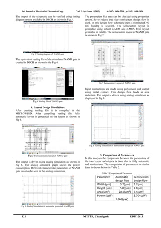
Bar chart representation of the parameters
The bar chart depicts that the area is reduced by using
semicustom technique by using almost same power.
5. CONCLUSION
This paper presents fully automatic and semicustom
techniques to optimize area and power in VLSI design.
The layout of NAND gate has been designed and
simulated using above mentioned techniques for area and
power comparison. Both the layouts have been simulated
using 90 nm technology. The simulated results show that
semicustom technique based NAND layout consumes 7.4
µm² area as compared to 28.5 µm² in case of fully
automatic NAND gate. It can be observed from the
simulated results that semicustom NAND gate consumes
1.7 µW power as compared to 1.6 µW in case of fully
automatic NAND gate.
REFERENCES
[1] Pushpa Saini, Rajesh Mehra, “Leakage Power Reduction in CMOS
VLSI circuits” International Journal of Computer Applications (0975-
8887), Volume 55-No. 8, October 2012
[2] Dinesh Sharma and Rajesh Mehra, “Low Power,Delay Optimized,
Buffer Design using 70 nm CMOS Technology, International Journal of
Computer Applications (0975-8887), Volume 22-No. 3, May 2011.
[3] Anjali Sharma, Richa Singh, Pankaj Kajla, “Area Efficient 1-Bit
Comparator Design by using Hybridized Full Adder Module based on
PTL and GDI Logic, Volume 82-No. 10, November 2013.
[4] Meena Aggarwal, Aastha Aggarwal, Mr. Rajesh Mehra, “4-Input
Decimal Adder Using 90 nm CMOS Technology”, IOSR Journal of
Engineering (IOSRJEN) e-ISSN:2250-3021,p-ISSN:2278-8719,VOL.3,
Issue 5(May. 2013), || v4 || PP 48-51.
[5] Prem Chandra Gupta, Rajesh Mehra, “Design of 8-Bit ALU using
Microwind 3.1, International Journal of Advanced Engineering Research
and Technology (IJAERT), Volume 2, Issue 2, May 2014, ISSN No.:
2348-8190.
[6] Vibha Soni, Nitin Naiyar, “Evaluation of Logic Families using NOR
and NAND Logic gates”,International Journal of Engineering and
Innovative Technology (IJEIT), Volume 3, Issue 7, January 2014.
[7] Neil Weste and David Harris, CMOS VLSI Design, Circuit and
System perspective, edition 3, Pg no. 8.
Acknowledgment
This research paper is made possible through the help and support
from everyone including parents, teachers and friends. Especially
I want to dedicate my acknowledgement of gratitude towards the
following significant advisors and contributors.
Firstly and foremost I would like to thank Mr. Rajesh Mehra for
his support, encouragement and to read my research paper and to
provide valuable guidance. The product of this research paper
would not be possible without all of them.
0
5
10
15
20
25
30
Automatic
Semicustom](https://image.slidesharecdn.com/id41-150525183232-lva1-app6891/85/Semi-custom-Layout-Design-and-Simulation-of-CMOS-NAND-Gate-3-320.jpg)

The document presents a study on the design and simulation of a CMOS NAND gate using 90 nm technology, comparing fully automatic and semicustom layout techniques. The semicustom approach resulted in a significant area reduction of 74%, while power consumption remained comparable between the two methods. The findings highlight the advantages of semicustom design in VLSI circuits for optimizing area and power efficiency.