Download to read offline
![International Journal of Engineering Research and Development
e-ISSN: 2278-067X, p-ISSN: 2278-800X, www.ijerd.com
Volume 11, Issue 01 (January 2015), PP.63-66
63
A 8-bit high speed ADC using Intel µP 8085
Gururaj Balikatti, Varalakshmi. V, Varalakshmi. G.U, Veda.M .V, Likhitha.S
Department of Electronics, Maharani’s Science College for Women, Bangalore-560001, Karnataka, India.
Abstract:- An 8-bit ADC Architecture of is proposed, it uses 16 comparators and produces 8-bit digital code in
half the time as that of successive approximation technique. In this approach, the analog input range is
partitioned into 16 quantization cells, separated by 15 boundary points. A 4-bit binary code 0000 to 1111 is
assigned to each cell. The results show that the ADC exhibits a maximum DNL of 0.49LSB and a maximum
INL of 0.51LSB.
Keywords:- ADC, Microprocessor, DAC, Sample and Hold. Successive approximation.
I. INTRODUCTION
Analog-to-digital converters (ADCs) are critical building blocks in a wide range of hardware from
radar and electronic warfare systems to multimedia based personal computers and work stations [1]. The need
constantly exists for converters with higher resolution, faster conversion speeds and lower power dissipation.
An N-bit flash architecture uses 2N-1
comparators, where N is the stated resolution. Flash converters often
include one or two additional comparators to measure overflow conditions [2].
All comparators sample the analog input voltage simultaneously. This ADC is thus inherently fast. The
Parallelism of the flash architecture has drawbacks for higher resolution applications. The number of
comparators grows exponentially with N, in addition, the separation of adjacent reference voltages grows
smaller exponentially, and consequently this architecture requires very large IC’s. It has high power dissipation.
Two step Flash converters are popular for conversion resolutions in the 8-12 bit range where optimized designs
can achieve low power dissipation and small silicon area for implementation [3, 4]. However, beyond such
resolution, the area and power dissipation of two-step Flash ADC’s nearly double for each additional bit of
resolution [5].
Typically high-resolution ADC’s have been based either on self-calibrated successive approximation
[6,7] or over sampling architectures [8, 9]. But both of these architectures are unsuitable for high speed
applications.
There are many different architectures like pipelined convertor [10, 11], successive approximation
convertor [12, 13], Sigma-Delta convertor [14], folding ADC’s [15], reported recently for high speed
applications. But these architectures have significant amount of complexity. In this paper an 8-bit Architecture
of analog-to-digital (A/D) converter is proposed to improve the sampling rate of an ADC. The prototype ADC
based on this technique uses only 17 comparators and needs only four comparisons, instead of eight
comparisons normally required in the conventional successive approximation techniques for 8-bit resolution.
This can increase the speed of conversion.
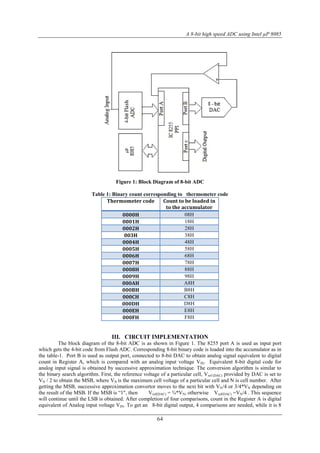
II. ADC ARCHITECTURE
The block diagram of the proposed 8-bit ADC is illustrated in Figure-1. It is based on a conventional
successive approximation technique. The ADC consists of an input sample and hold amplifier (SHA), 4-bit
flash ADC, 8-bit DAC, 8-bit µP 8085 and some extra supporting circuit blocks. 4-bit flash ADC partitions
input range into 16-quantization cells. From the 4-bit code µP8085 decides within which cell the input sample
lies. This gives 4 MSB bits 0000 to 1111 according to the cell value. Remaining 4 bits are obtained by
successive approximation technique.
A binary count is loaded into the Register A depending on the 4-bit code. The detailed binary count to
be loaded for different code is summarized in table-1.
The Analog to digital converter is designed and developed using µP8085.
The 4-bit code generated by 4-bit flash ADC is fed to Port A of 8255. Depending on the code value, a binary
count is loaded in Register A as given in table -1. The successive approximation technique is used to get a final
8-bit digital code for the analog input signal.](https://image.slidesharecdn.com/i11016366-150408051029-conversion-gate01/85/A-8-bit-high-speed-ADC-using-Intel-P-8085-1-320.jpg)
![International Journal of Engineering Research and Development
e-ISSN: 2278-067X, p-ISSN: 2278-800X, www.ijerd.com
Volume 11, Issue 01 (January 2015), PP.63-66
63
A 8-bit high speed ADC using Intel µP 8085
Gururaj Balikatti, Varalakshmi. V, Varalakshmi. G.U, Veda.M .V, Likhitha.S
Department of Electronics, Maharani’s Science College for Women, Bangalore-560001, Karnataka, India.
Abstract:- An 8-bit ADC Architecture of is proposed, it uses 16 comparators and produces 8-bit digital code in
half the time as that of successive approximation technique. In this approach, the analog input range is
partitioned into 16 quantization cells, separated by 15 boundary points. A 4-bit binary code 0000 to 1111 is
assigned to each cell. The results show that the ADC exhibits a maximum DNL of 0.49LSB and a maximum
INL of 0.51LSB.
Keywords:- ADC, Microprocessor, DAC, Sample and Hold. Successive approximation.
I. INTRODUCTION
Analog-to-digital converters (ADCs) are critical building blocks in a wide range of hardware from
radar and electronic warfare systems to multimedia based personal computers and work stations [1]. The need
constantly exists for converters with higher resolution, faster conversion speeds and lower power dissipation.
An N-bit flash architecture uses 2N-1
comparators, where N is the stated resolution. Flash converters often
include one or two additional comparators to measure overflow conditions [2].
All comparators sample the analog input voltage simultaneously. This ADC is thus inherently fast. The
Parallelism of the flash architecture has drawbacks for higher resolution applications. The number of
comparators grows exponentially with N, in addition, the separation of adjacent reference voltages grows
smaller exponentially, and consequently this architecture requires very large IC’s. It has high power dissipation.
Two step Flash converters are popular for conversion resolutions in the 8-12 bit range where optimized designs
can achieve low power dissipation and small silicon area for implementation [3, 4]. However, beyond such
resolution, the area and power dissipation of two-step Flash ADC’s nearly double for each additional bit of
resolution [5].
Typically high-resolution ADC’s have been based either on self-calibrated successive approximation
[6,7] or over sampling architectures [8, 9]. But both of these architectures are unsuitable for high speed
applications.
There are many different architectures like pipelined convertor [10, 11], successive approximation
convertor [12, 13], Sigma-Delta convertor [14], folding ADC’s [15], reported recently for high speed
applications. But these architectures have significant amount of complexity. In this paper an 8-bit Architecture
of analog-to-digital (A/D) converter is proposed to improve the sampling rate of an ADC. The prototype ADC
based on this technique uses only 17 comparators and needs only four comparisons, instead of eight
comparisons normally required in the conventional successive approximation techniques for 8-bit resolution.
This can increase the speed of conversion.
II. ADC ARCHITECTURE
The block diagram of the proposed 8-bit ADC is illustrated in Figure-1. It is based on a conventional
successive approximation technique. The ADC consists of an input sample and hold amplifier (SHA), 4-bit
flash ADC, 8-bit DAC, 8-bit µP 8085 and some extra supporting circuit blocks. 4-bit flash ADC partitions
input range into 16-quantization cells. From the 4-bit code µP8085 decides within which cell the input sample
lies. This gives 4 MSB bits 0000 to 1111 according to the cell value. Remaining 4 bits are obtained by
successive approximation technique.
A binary count is loaded into the Register A depending on the 4-bit code. The detailed binary count to
be loaded for different code is summarized in table-1.
The Analog to digital converter is designed and developed using µP8085.
The 4-bit code generated by 4-bit flash ADC is fed to Port A of 8255. Depending on the code value, a binary
count is loaded in Register A as given in table -1. The successive approximation technique is used to get a final
8-bit digital code for the analog input signal.](https://image.slidesharecdn.com/i11016366-150408051029-conversion-gate01/75/A-8-bit-high-speed-ADC-using-Intel-P-8085-1-2048.jpg)
![A 8-bit high speed ADC using Intel µP 8085
65
comparisons in the normal successive approximation ADC. Finally 8-bit digital code is available at port C.
Software for implementing successive approximation converter in µP8085 is written in assembler code.
IV. MEASURED RESULT
An experimental prototype of 8-bit ADC using proposed technique was designed and developed using
µP8085. The working functionality of the ADC has been checked by generating a ramp input going from 0 to
3.5V (full scale range of the ADC). Digital codes have been obtained correctly, going from 0 to 255 for 8-bit
at the output, indicating that the ADC’s working is functionally correct. Both the differential and integral
nonlinearities (DNL and INL) were measured over 28
output codes by applying slowly varying full scale range
ramp as input to the proposed ADC, which completes the full scale range in 255 steps .The values of the each
code are compared with ideal value and store the difference value. The results show that the ADC exhibits a
maximum DNL of 0.49LSB and a maximum INL of 0.51LSB as shown in the Figures 2(a) and 2(b).
Figure 2(a): DNL Versus output Code Figure 2(b): INL Versus output Code
V. CONCLUSION
We have presented a simple and effective technique for enhancing speed of a successive approximation
ADC. This technique would be effective in a large number of high speed controls and signal processing
applications such as hard-disk-drive read Chanel and wireless receivers. Although these applications are most
often implemented with Flash convertors, but these ADC’s demands larger power. Also, the ADC die area and
power dissipation increase exponentially with resolution, limiting the resolution of such ADC’s less than 10bits.
This paper shows that partitioning analog input range increases the conversion rate of successive approximation
ADC’s. The main conclusion is that although Flash convertors provide high conversion rates, required power
dissipation of these ADC’s are large. Also, resolution beyond 10bits these ADC’s become prohibitively
expensive and bulky. Proposed technique provides high enough conversion speed for high speed applications,
with less power dissipation even beyond 10bit resolution.
Implementation of successive approximation algorithm in Microprocessor has reduced the hardware
requirement and cost. Proposed technique uses only 16 comparators to enhance speed of 8-bit successive
approximation ADC by 50%.
REFERENCES
[1]. P.E.Pace, J.L. Schaler, and D.Styer, “Optimum Analog preprocessing for folding ADC’s”, IEEE Trans.
Circuits System-II, Vol.42.pp.825-829, Dec. 95.
[2]. Robert H.Walden, “Analog-to-Digital Converter Survey and Analysis”, IEEEJ.Comm. Vol.17, No.4,
pp539-549, April 1999.
[3]. B.Razavi and B.A.Wooley, “A 12-b 5-M samples Two-step CMOS A/D converter”, IEEE J. Solid-
State circuits, Vol. 27, Dec.1992, pp.1667-1678.
[4]. B.S.Song, S.H.Lee, and M.F.Tompsett, “ A10-b 15-MHz CMOS recycling two steps A/D converter”,
IEEE J. Solid-state circuits,Vol. 25, Dec.1990, pp. 1328-1338.
[5]. Joao Goes, Joao C. Vital, and Jose E.France “Systematic Design for optimization of High Speed Self-
Calibrated Pipelined A/D converters”, IEEE Trans. Circuits system II, Dec 1998, Vol. 45, pp.1513-
1526.
[6]. H.S.Lee. D.Hodges, and P.R.Gray, “A self-calibrating 15 bit CMOS A/D converter”, IEEE J. Solid
state circuits Vol. SC-19, Dee.1984, pp.813-819.
[7]. M.de Wif, k-s. Tan, R.K.Hester,A low-power 12-b analog-to-digital converter with on-chip precision
trimming”, IEEE J. Solid-state circuits. Vol. 28, Apr.1933, pp.455-461.](https://image.slidesharecdn.com/i11016366-150408051029-conversion-gate01/85/A-8-bit-high-speed-ADC-using-Intel-P-8085-3-320.jpg)
![A 8-bit high speed ADC using Intel µP 8085
66
[8]. K.S.Tan. S.Kiriaki, M.De Wit, J.W.Fattaruso, C.Y.Tayet al “Error correction techniques for high-
performance differential A/D converters”, IEEE J. Solid-state circuits, Vol. 25, Dec.1990, pp.1318-
1326.
[9]. J.W.Fattaruso, S.Kiriaki, M.Dewit, and G.Waxwar. “Self-Calibration techniques for a second-order
multi bit sigma-delta modulator”, IEEE J. Solid-state circuits, Vol. 28, Dec.1993, pp.1216-1223.
[10]. M.M. Furuta, M. Nozawa, and T. Itakura, “A 10-bit, 40-MS/s, 1.21mW Pipelined SAR Using
Single Ended 1.5-bit/ cycle Conversion Technique”, IEEE J. Solid State Circuits, Vol. 46, No.6, June
2011, pp.1360-1370.
[11]. H. Lee, -Y, “Zero-Crossing-based 8-bit 100 MS/s Pipelined analog-to-digital Convertor with offset
Compensation”, IET Circuits, Devices & Systems, Vol. 5, No. 5, Sept. 2011, pp. 411- 417.
[12]. G. Harish, S. Prabhu, and P. Cyril Prasanna Raj, “Power Effective Cascaded Flash-SAR Sub ranging
ADC”, IJTES, Vol. 2, No. 3, Jan-Mar 2011, pp. 306-308.
[13]. Sang-Hyun Cho, Chang-Kyo Lee, Jong-Kee Kwon, and Seung-Tak Ryu, “A 550µW, 10-bit 40 MS/s
SAR ADC with Multistep Addition- only Digital Error Correction”, IEEE J. Solid-State Electronics,
Vol. 46, No. 8, Aug. 2011, pp. 1881- 1892.
[14]. Yan Wang, P. K. Hanumolu, and G. C. Temes, “Design Techniques for Wideband Discrete-time Delta-
Sigma ADC’s with Extra Loop Delay”, IEEE Trans. Circuits system I, July 2011, Vol. 58, No. 7,
pp.1513-1526.
[15]. Oktay Aytar and Ali Tangel, “Employing threshold inverter quantization(TIQ) technique in designing
9-bit folding and interpolation CMOS analog-to-digital converters(ADC)”, SRE, Vol. 6(2), Jan. 2011,
pp. 351- 362.](https://image.slidesharecdn.com/i11016366-150408051029-conversion-gate01/85/A-8-bit-high-speed-ADC-using-Intel-P-8085-4-320.jpg)

The document presents an 8-bit high-speed analog-to-digital converter (ADC) architecture using the Intel μP 8085 microprocessor, which employs 16 comparators and a modified successive approximation technique to enhance conversion speed. The proposed ADC achieves significant improvements by reducing the number of comparisons needed for conversion from the conventional eight to four, resulting in a maximum differential nonlinearity (DNL) of 0.49 LSB and integral nonlinearity (INL) of 0.51 LSB. The technique aims to meet the demands of high-speed applications while minimizing power dissipation and hardware complexity.


![Getting Started with Apache Spark: Big Data Made Simple [Free Meetup]](https://cdn.slidesharecdn.com/ss_thumbnails/apachesparkgettingstarted-260203175547-8361bcc3-thumbnail.jpg?width=640&height=640&fit=bounds)


