Downloaded 64 times


![Reference
• [1] Design & Implementation of Low Power 3-bit Flash ADC in
0.18µm CMOS, Pradeep Kumar, Amit Kolhe, international Journal
of Soft Computing and Engineering (IJSCE)ISSN: 2231-2307,
Volume-1, Issue-5, November 2011.
• [2] https://en.wikipedia.org/wiki/Comparator
• [3] http://www.electronics-tutorials.ws/combination/comb_4.html
• [4] Design of a new 3-bit Flash Analog to Digital Converter
(ADC)E. O. Ogunti and F. J. OmotayoDepartment of
Electrical/Electronic Engineering Federal University of Technology,
Akure, Nigeria](https://image.slidesharecdn.com/designflashadc-150709021816-lva1-app6891/85/Design-flash-adc-3bit-VHDL-design-19-320.jpg)


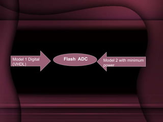
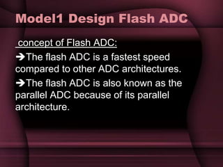
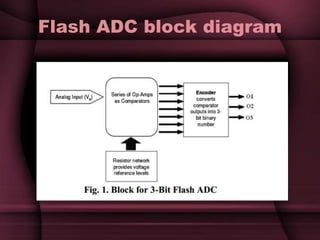
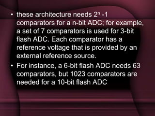
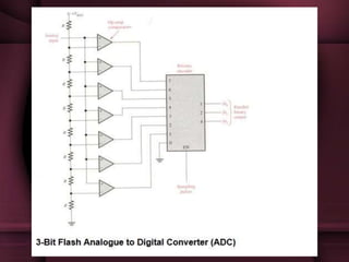
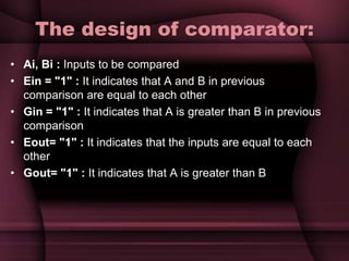
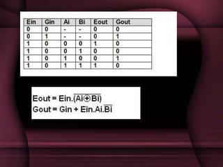
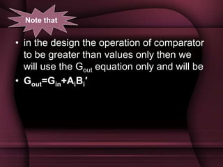
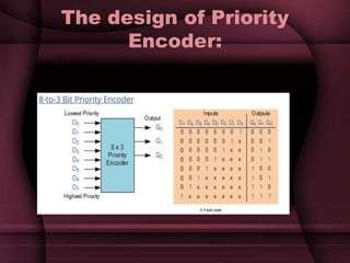
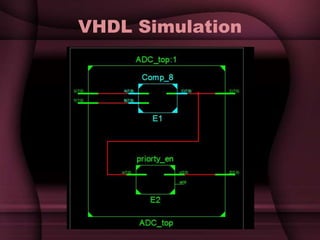
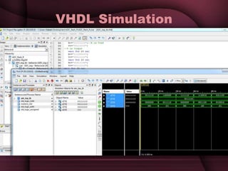
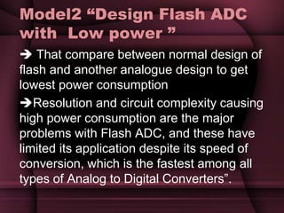
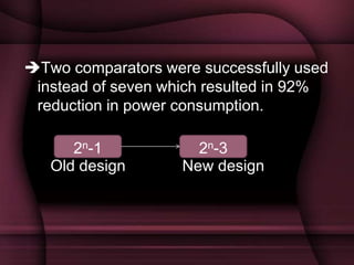
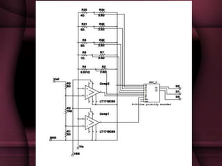
This document discusses the design of a 3-bit flash analog-to-digital converter (ADC). It begins by introducing flash ADCs and their advantages of high speed. A flash ADC uses 2n-1 comparators in parallel to convert an analog input to an n-bit digital code. The document then describes modeling a 3-bit flash ADC in VHDL, including the design of comparators using inputs A and B, and outputs for equal and greater signals. It also covers the use of a priority encoder. Finally, the document discusses another design approach to reduce power consumption by using fewer comparators.


![[Deck] What's New in Spark-Iceberg Integration via DSV2.pptx](https://cdn.slidesharecdn.com/ss_thumbnails/deckwhatsnewinspark-icebergintegrationviadsv2-260210005337-25955b12-thumbnail.jpg?width=640&height=640&fit=bounds)


