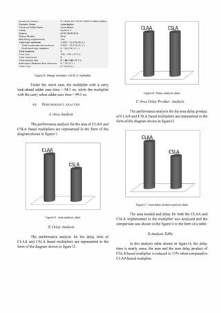
This document compares the design and implementation of 32-bit unsigned integer multipliers using carry look-ahead adders (CLAA) and carry select adders (CSLA). It finds that a CSLA-based multiplier has 31% less area than a CLAA-based multiplier, while both achieve nearly the same delay time of 99ns. VHDL models are developed and simulated for both multipliers. Analysis shows the CSLA design has better area efficiency with comparable speed performance.
![Let Gi is the carry generate function and Pi be the
carry propagate function, Then we can rewrite the carry
function as follows:
Gi = Ai· Bi.
Pi = (Ai xor Bi).
Si = Pi xor Ci.
Ci+l= Gi + Pi.Ci.
(1)
(2)
(3)
(4)
In general, we can write the algorithm as:
If Carry in =1, then the sum and carry out are given by,
Sum (i) =a (i) xor b (i) xor '1'.
Carry (i+1) = (a (i) and b (i)) or (b (i) or a (i)).
If Carry in =0, then the sum and carry out are given by,
Sum (i) = a (i) xor b (i).
Carry (i+1) = (a (i) and b (i)).
Thus, for 4-bit adder, we can compute the carry for
all the stages as shown below:
(5)
C 1 = Go + Po.Co.
C2 = G 1 + P 1 .C 1 = G 1 + P 1.GO + P 1 .PO.CO (6)
C3 = G2 + P2 .C2 = G2 + P2.G 1 + P2.P I.GO
+ P2.P 1.PO.CO
(7)
C4 = G3 + P3.C3 = G 3 + P3.G 2 + P3.P2 .G 1 + P3.P2.P 1.GO
(8)
+ P3.P2.Pl.PO.CO
(11)
(12)
(13)
(14)
The sum function:
(IS)
The carry function:
(16)
In general, we can write:
The sum function:
IV.
(9)
The carry function:
Ci+l= Gi + Pi.Ci.
TTL
(10)
MUL TIPLTER FOR UNSIGNED DATA
Multiplication involves the generation of partial
products, one for each digit in the multiplier, as in
Figure3.These partial products are then summed to produce
the final product. The multiplication of two n-bit binary
integers results in a product of up to 2n bits in length [2].
CARRY SELECT ADDER
b (0)
The concept of CSLA is to compute alternative
results in parallel and subsequently selecting the correct
result with single or multiple stage hierarchical techniques.
In CSLA both sum and carry bits are calculated for two
alternatives Cin=O and 1. Once Cin is delivered, the correct
computation is chosen using a mux to produce the desired
output. Instead of waiting for Cin to calculate the sum, the
sum is correctly output as soon as Cin gets there. The time
taken to compute the sum is then avoided which results in
good improvement in speed.
Cin
b (1)
b (2)
b (31)
32
roj(63 downto 32)
prod(31 )
[lrod(O)
Figure3. A partial schematic ofthe multiplier
S7:4
Figure2. Carry Select Adder
5:3:0
We used the following algorithm to implement the
multiplication operation for unsigned data.](https://image.slidesharecdn.com/10-140225064129-phpapp01/85/implementation-and-design-of-32-bit-adder-2-320.jpg)
![v.
MULTIPLICATION ALGORITHM
40.0ns
500ns
Let the product register size be 64 bits. Let the
multiplicand registers size be 32 bits. Store the multiplier in
the least significant half of the product register. Clear the
most significant half of the product register.
Repeat the following steps for 32 times:
1. If the least significant bit of the product register is "1"
then add the multiplicand to the most significant half of the
product register.
2. Shift the content of the product register one bit to the right
(ignore the shifted-out bit.)
3. Shift-in the carry bit into the most significant bit of the
product register. Figure 4.Shows a block diagram for such a
multiplier [2].
X
X
3782682799
1404927549
531439527344 3529651
)
)
3048485111
1
718766224761576960
3
1908060884
+
1699019376
X
I
1
4230476960
5816695195755493124
)
FigureS. Waveform for a CLAA based multiplier
40.0ns
5O.0ns
I
1404927549
1
1699019376
t
7187662324761576960
3782682799
601
I
5314395273443529651
Multiplicand
601
I
I
I
X
X
4230476S60
3048485111
1908060884
X
5816695195755493124
Figure6. Waveform for a CSLA based multiplier
Timing Analyzer Summary
Shll'land Add
Con 11'01
Lugie
ReqJred
Type
..
Slack Time
.
1 Worst·case t�
�/A
I�� If IT
rom
Tine
0
I
To
from
F��d
C� Cb:k P�tm
T9Il.5b5�a[3] -"-lIl{S:3] .. }
Nooe
0
Figure7. Timing Analysis for CLAA based multiplier
Timing Analyzer Summary
Slack
I Worst·case tpd
VHDL SIMULATIONS
None
From To
99.553 m all]
Quartus
II Version
suml63] ..
8.1 Build 163 1012812008
Revision Name
..
0
CLAmultiplier
Family
Cyclone
Device
SJ Web Ed�ion
CLAmuttiplier
Top-level Entrty Name
The VHDL simulation of the two multipliers is
presented in this section. Tn this, waveforms, timing
diagrams and the design summary for both the CLAA and
CSLA based multipliers are shown in the figures. The
VHDL code for both multipliers, using CLAA and CSLA,
are generated. The VHDL model has been developed using
Altera Quartus IT and timing diagrams are viewed through
avan waves. The multipliers use two 32-bit values.
From To
Failed
Clock Clock Paths
FigureS. Timing Analysis for CSLA based multiplier
Figure4. Multiplier of two n-bit values.
VI.
Required Actual
Time
Time
NIA
Type
EP=35F672C6
II
Timing Models
Rnal
Met timing requirements
Yes
Total logic elements
2.957/33.216(9%)
Total combinational functions
2.957 I 33.216 (9%)
Dedicated logic registers
0/ 33.216(0%)
Total registers
0
Total pins
129/475(27%)
Total virtual pins
0
Total memory b�s
0/48.3.840 (0%)
Embedded Multiplier 9-bit elements
0/ 70 ( 0%)
Total PLLs
0/4(0%)
Figure9. Design summary ofCLAA multiplier
j.](https://image.slidesharecdn.com/10-140225064129-phpapp01/85/implementation-and-design-of-32-bit-adder-3-320.jpg)
![Figurel4. Analysis Table
[4]
A. Sertbas and R.S. Ozbey, "A performance analysis of classified
binary adder architectures and the VHDL simulations",
J Elect.
Electron. Eng., Istanbul,Turkey,vol. 4,pp. 1025-1030,2004.
Multiplier type
Delay
(ns)
Area
Delay Area
Product
[5]
based
multiplier
CSLA
2957
98. 5
logic
291264.5
multiplier
logic
of Technology,
S. Brown and
Z. Vranesic, Fundamentals of Digital Logic with VHDL
0072499389.
[7]
2039
99. 5
Institute
Design, 2nd ed. , McGraw-Hill Higher Education, USA, 2005. ISBN:
cells
based
Thesis. National
Rourkela, 2009.
[6]
CLAA
P. S. Mohanty, "Design and Implementation of Faster and Low Power
Multipliers", Bachelor
J. R. Armstrong and F.G. Gray, VHDL Design Representation and
Synthesis, 2nd ed. ,Prentice Hall, USA, 2000. ISBN: 0-13-021670-4.
202880.5
[8]
cells
Z. Navabi, VHDL Modular Design and Synthesis of Cores and
Systems, 3rd ed. , McGraw-Hill Prof
essional, USA, 2007.
ISBN:
9780071508926.
[9]
VITI.
P.
C. H.
Meier, R.
A.
Rutenbar and L.
[10] Software Simulation Package:
A design and implementation of a VHDL-based 32bit unsigned multiplier with CLAA and CSLA was
presented. VHDL, a Very High Speed Integrated Circuit
Hardware Description Language, was used to model and
simulate our multiplier. Using CSLA improves the overall
performance of the multiplier.
Thus a 31% area delay product reduction is
possible with the use of the CSLA based 32 bit unsigned
parallel multiplier than CLAA based 32 bit unsigned parallel
multiplier.
R.
Carley, "Exploring
Multiplier Architecture and Layout for low Power",CIC'96,1996.
CONCLUSION
Direct VHDL, Version 1.2, 2007,
Green Mounting Computing Systems, Inc., Essex, VT, UK.
[II] Hasan Krad and Aws Yousi( "Design and Implementation of a Fast
Unsigned 32-bit Multiplier Using VHDL",20IO.
Dr.S.Ramakrishnan was born in Tirunelveli, India in
1969.
He
received his Bachelors of Engineering degree fi'om the deprniment
of Electronics and Instrumentation fi'om Annamalai University,
Chidambaram, India and Masters Degree & Ph.D in Electrical
Engineering fi'om Anna University, Chennai India. He has over
years of
5
teaching experience after
15
years experience in the
industry. He is currently working as Principal & HeadlDeprniment
of
IT
in
Sakthi MrnTiamman Engineering
College,
Chennai,
India.He is the member of IEEE & IETE. He has published in many
peer refelTed international and national journals and conferences.
IX.
FUTURE WORK
This 32 bit multiplier can be further extended to 64
bit multiplier and 128 bit multiplier using the proposed
method for multiplication operation can be done as future
work.
REFERENCES
[I]
P. Asadi and K. Navi, "A novel highs-speed 54-54 bit multiplier",
Am.
[2]
J Applied Sci., vol. 4 (9), pp. 666-672. 2007.
W. Stallings, Computer Organization and Architecture Designing for
Peljormance, 71h ed., Prentice Hall, Pearson Education International,
USA,2006,ISBN: 0-13-185644-8.
[3]
1. F. Wakerly, Digital Design-Principles and Practices, 4th ed. ,
Pearson Prentice Hall,USA, 2006. ISBN: 0131733494.
received
Mr.R.Seshadri
Electronics
and
the B.E and M.E degrees,
communication
engineering
fi'om
both in
the
S.K.P
Engineering College, Tiruvannamalai, Tamilnadu, India. He has
doing the Ph.D degree in Digital Signal Processing Architecture
at Anna University, India. Currently, he is working as a Assistant
Professor
in
Arunai
Engineering
Tamilnadu, India. He has having
V.Vijayalakshmi
was
born
College,
Tiruvannamalai,
4 years of teaching Experience.
on
October
12,
1990
in
Tiruvannamalai, Tamilnadu, India. She has received the B.E degree
in Electrical and Electronics Engineering from Arunai College of
Engineering, Anna University, Chennai, Tamilnadu, India, in May
2011.
She is currently pursuing her M.E degree in Applied
Electronics fi'om Arunai Engineering College, Anna University,
Chennai, Tamilnadu, India from
journal
in
National
2011
conference
to
2013.
She has published a
conducted
Chockalingam Engineering College on January,
interest include VLSI and Control Systems.
by
2013.
Sri
Balaji
Her areas of](https://image.slidesharecdn.com/10-140225064129-phpapp01/85/implementation-and-design-of-32-bit-adder-5-320.jpg)