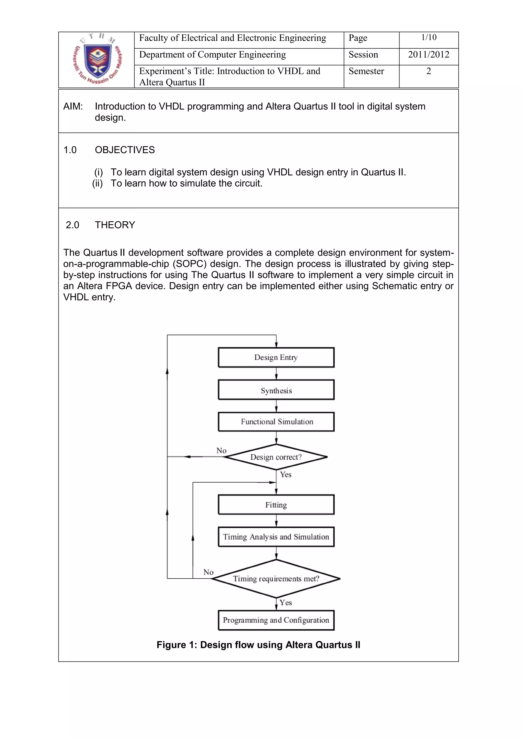
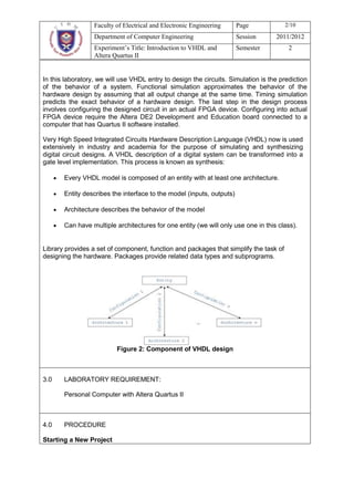
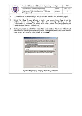
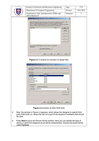
Faculty of Electrical and Electronic Engineering   Page             1/10
                  Department of Computer Engineering                 Session        2011/2012
                  Experiment’s Title: Introduction to VHDL and       Semester          2
                  Altera Quartus II

AIM:   Introduction to VHDL programming and Altera Quartus II tool in digital system
       design.


1.0    OBJECTIVES

        (i) To learn digital system design using VHDL design entry in Quartus II.
       (ii) To learn how to simulate the circuit.


2.0    THEORY

The Quartus II development software provides a complete design environment for system-
on-a-programmable-chip (SOPC) design. The design process is illustrated by giving step-
by-step instructions for using The Quartus II software to implement a very simple circuit in
an Altera FPGA device. Design entry can be implemented either using Schematic entry or
VHDL entry.


                      Figure 1: Design flow using Altera Quartus II
Faculty of Electrical and Electronic Engineering     Page            2/10
                  Department of Computer Engineering                   Session     2011/2012
                  Experiment’s Title: Introduction to VHDL and         Semester         2
                  Altera Quartus II


In this laboratory, we will use VHDL entry to design the circuits. Simulation is the prediction
of the behavior of a system. Functional simulation approximates the behavior of the
hardware design by assuming that all output change at the same time. Timing simulation
predicts the exact behavior of a hardware design. The last step in the design process
involves configuring the designed circuit in an actual FPGA device. Configuring into actual
FPGA device require the Altera DE2 Development and Education board connected to a
computer that has Quartus II software installed.

Very High Speed Integrated Circuits Hardware Description Language (VHDL) now is used
extensively in industry and academia for the purpose of simulating and synthesizing
digital circuit designs. A VHDL description of a digital system can be transformed into a
gate level implementation. This process is known as synthesis:

       Every VHDL model is composed of an entity with at least one architecture.

       Entity describes the interface to the model (inputs, outputs)

       Architecture describes the behavior of the model

       Can have multiple architectures for one entity (we will only use one in this class).


Library provides a set of component, function and packages that simplify the task of
designing the hardware. Packages provide related data types and subprograms.


                          Figure 2: Component of VHDL design


3.0    LABORATORY REQUIREMENT:

       Personal Computer with Altera Quartus II


4.0    PROCEDURE

Starting a New Project
Faculty of Electrical and Electronic Engineering   Page             3/10
                 Department of Computer Engineering                 Session       2011/2012
                 Experiment’s Title: Introduction to VHDL and       Semester          2
                 Altera Quartus II

1.   To start working on a new design, first you have to define a new designed project.

2.   Select File | New Project Wizard to start a new project. Press Next to get the
     window shown in Figure L1. Set the working directory to be
     C:No.MatrikLAB1halfadd. The project must have a name, which may optionally be
     the same as the name of the directory.

3.   Name your project as halfadd and press Next which leads to the window in Figure L2.
     In this window the designer can specify which existing files (if any) should be included
     in the project. We have no existing files, so click Next.


                        C:No.MatrikLAB1halfadd


                        halfadd


                        halfadd


                   Figure L1 Specifying the project directory and name
Faculty of Electrical and Electronic Engineering   Page              4/10
                 Department of Computer Engineering                 Session        2011/2012
                 Experiment’s Title: Introduction to VHDL and       Semester           2
                 Altera Quartus II


                     Figure L2: A window for inclusion of design files


                          Figure L3 Inclusion of other EDA tools

4.   Now, the window in Figure L3 appears, which allows the designer to specify third
     party CAD tools (i.e. those that are not a part of the Quartus II software) that should
     be used.

5.   Press Next to go to the Device Family window. Here you can specify the type of
     device in which the designed circuit will be implemented. Choose the device family
     called Cyclone.
Faculty of Electrical and Electronic Engineering      Page               5/10
                  Department of Computer Engineering                    Session        2011/2012
                  Experiment’s Title: Introduction to VHDL and          Semester            2
                  Altera Quartus II

6.   Then click Finish.


Part A: Design Half Adder Using VHDL
In this section, you will use Quartus II to implement logic functions by writing VHDL code.
The half adder is the simplest of the two adder circuits and is capable of adding together two
bits.

Circuit specification
1.   The circuit has two inputs: the two bits that will be added (referred to as “A” and “B”).

2.   The circuit has two outputs: a sum output (referred to as “Sum”) and a carry out output
     (referred to as “Cout”).

3.   The circuit specification is such that the “Sum” output will be 1 when either one (but not
     both) of inputs “A” or “B” are 1; otherwise it will be 0. The “Cout” output will be 1 only
     when both input “A” and “B” are 1; otherwise it will be 0.

4.   This can be represented in the form of a truth table as shown in Table A1.

                             Table A1: Truth table for half adder
                          Inputs                            Outputs
                  A                 B               Sum                   Cout
                  0                 0                0                     0
                  0                 1                1                     0
                  1                 0                1                     0
                  1                 1                0                     1


5.   From the truth table, we can construct the following Boolean expressions for “Sum” and
     “Cout”;
                                 Sum      A B    A B     A    B
                                 Cout     A B

6.   It can be seen that “Sum” can be obtained by performing an XOR operation on “A” and
     “B”, and that “Cout” can be obtained by performing an AND operation on “A” and “B

Design Entry
2.   Create a new project for the VHDL design in the directory C:LAB1 halfadd. Name
     the new project as halfadd and choose the device family called Cyclone.

3.   Select File | New, choose VHDL File, and click OK. This opens the Text Editor
     window. The first step is to specify a name for the file that will be created. Select File |
     Save As to open the Save As pop-up window. In the box labeled File name type
     halfadd. (Make sure that the extension is VHDL File). Leave the box checked at the
Faculty of Electrical and Electronic Engineering   Page             6/10
                 Department of Computer Engineering                 Session       2011/2012
                 Experiment’s Title: Introduction to VHDL and      Semester           2
                 Altera Quartus II
     bottom of the window, which specifies Add File to current project.

4.   Enter the code shown in Figure A1 into the Text Editor window. (Make sure that entity
     name must be same as file name, in this case, halfadd).

                  LIBRARY ieee;
                  USE ieee.std_logic_1164.all;

                  ENTITY halfadd IS
                  PORT (A, B : IN std_logic;
                  Sum, Cout : OUT std_logic);
                  END halfadd;

                  ARCHITECTURE myadd OF halfadd IS
                  BEGIN
                  Sum <= A xor B;
                  Cout <= A and B;
                  END myadd;
                            Figure A1: VDHL code for half adder


5.   Save the file, by using File | Save or shortcut Ctrl-s.

6.   Now synthesize your code by select Processing | Start | Start Analysis and
     Synthesis.

7.   Run the Compiler by selecting Processing | Start Compilation. Successful (or
     unsuccessful) compilation is indicated in a pop-up box. View the report by selecting
     Processing | Compilation Report. If the compilation is unsuccessful, expand the
     Analysis & Synthesis part of the report and then select Messages to have the
     Messages displayed. Double-click on the first error message. Quartus II software
     responds By opening the VHDL file and highlighting the statement which is affected
     by the error. Correct the error and recompile the design.

(Q1) Sketch the functional block diagram for VHDL code in figure A1.(5 marks)

8.   Perform the functional and timing simulation, verify and discuss your result in the
     report. Before the circuit can be simulated, it is necessary to create the desired
     waveforms, called test vectors, to represent the input signals.

     a. Open the Waveform Editor window by selecting File | New. Click on the Other
        Files tab. Choose Vector Waveform File and click OK.

     b. The Waveform Editor window will appear. Save the file under the name
        halfadd.vwf.

     c. Set the desired simulation to run from 0 to 160 ns by selecting Edit | End Time
        and entering 160 ns in the dialog box that pops up. Select View | Fit in Window
        to display the entire simulation range of 0 to 160 ns in the window.

     d. Next, you must include the input and output nodes of the circuit to be simulated.
Faculty of Electrical and Electronic Engineering   Page              7/10
                   Department of Computer Engineering                 Session        2011/2012
                   Experiment’s Title: Introduction to VHDL and     Semester         2
                   Altera Quartus II
          This is done by using the Node Finder utility. Click Edit | Insert Node or Bus to
          open the Insert Node or Bus window.

     e. Click Node Finder… button to list out all nodes in the circuit. Since we are
        interested in input and output pins, set the filter to Pins: all. Click the List button
        to find the input and output nodes.

     f.   Double click on A, B, Sum and Cout to add it to the Selected Nodes box on the
          right side of the window. Click OK, this leaves a fully displayed Waveform Editor
          window.

     g. We will now specify the logic values to be used for the input signal during
        simulation. The logic values at the output Sum and Cout will be generated
        automatically by the simulator.

     h. To assign the value to the A, (let apply a new valuation every 20 ns.) click on A;
        this highlights the signal and activates the vertical toolbar that allow you to shape
        the selected waveform The toolbar provides options such as setting the signal to
        0, 1, unknown (X), high impedance (Z), don’t care (DC), and inverting its existing
        value (INV).

     i.   Select the interval from 20 to 40 ns for B and set the signal to 1. Finally, set A to 1
          from 40 to 80 ns.

     j.   A circuit can be simulated in two ways. The simplest way is to assume that logic
          elements and interconnection wires are perfect, thus causing no delay in
          propagation of signals through the circuit. This is called functional simulation. To
          perform the functional simulation, select Assignments | Setting to open the
          Settings window. On the left side of this window, click on Simulator and choose
          Functional as the simulation mode. Click OK and save the waveform as
          halfadd.vwf.

     k. To complete the set up of the simulator select the command Processing |
        Generate Functional Simulation Netlist.

     l.   Run the simulation process by select Processing | Start Simulation. After the
          simulation process is completed, press open to view the simulation result.

(Q2) Sketch your functional simulation waveform as a result for VHDL code in
     figure A1. (4 marks)

     m. The second way is called timing simulation. This simulation process use to
        examine the functionality of the circuit, and determine its speed of operation in the
        chosen device. Select Assignments | Setting | Simulator and choose Timing as
        the simulation mode. Run the simulator.


(Q3) Sketch your timing simulation waveform as a result for VHDL code in figure A1.
     (4 marks)
(Q4) What is the difference between function and timing waveform? (4 marks)
Faculty of Electrical and Electronic Engineering      Page               8/10
                     Department of Computer Engineering                    Session        2011/2012
                     Experiment’s Title: Introduction to VHDL and          Semester            2
                     Altera Quartus II

Part B: Full Adder Circuit
Part A of this experiment examined the half adder circuit, which as was seen added two bits
together and gave a sum output and a carry out output. This can therefore be thought of as a
circuit that adds two one-bit binary numbers together. To add another binary numbers larger
than one bit in size, a half adder circuit can be used to add together the two least significant bits
from each number.

Circuit Specification
1.    This full adder circuit has three inputs, the two bits that will be added (referred to as “A”
      and “B”) and a carry in bit (referred to as “Cin”).

2.    The outputs are “Sum” and “Cout”, as in the case with the half adder circuit.

3.    The circuit specification is such that the “Sum” output will be “1” when any one or all three
      of the inputs “A”, “B” and “Cin” are “1”; otherwise it will be “0”. The “Cout” output will be “1”
      when any two or all three of the inputs A, B and Cin are “1”; otherwise it will be “0”.


4.    This can be represented in the form of truth table as shown in Table B1.

                                Table B1: Truth table for full adder
                                  Inputs                             Outputs
                 A               B             Cin              Sum          Cout
                 0               0               0               0            0
                 0               0               1               1            0
                 0               1               0               1            0
                 0               1               1               0            1
                 1               0               0               1            0
                 1               0               1               0            1
                 1               1               0               0            1
                 1               1               1               1            1

(Q5) From the truth table, obtain the Boolean expression for Sum and Cout. Show
     your work clearly (8 marks). Then, draw the Full Adder circuitry? (5 marks)


Design Entry
1.    Create a new project for the VHDL design in the directory C:LAB1fulladd. Name
      the new project as fulladd and choose the device family called Cyclone.

2.    Repeat the procedure in Part A, 1 – 8, to design the Full Adder based on your answer
      in Q5. Save the file as a fulladd.vhd.


(Q6) Sketch your functional simulation waveform as a result for full adder (5 marks).
Faculty of Electrical and Electronic Engineering   Page         9/10
                 Department of Computer Engineering                 Session    2011/2012
                 Experiment’s Title: Introduction to VHDL and       Semester      2
                 Altera Quartus II

(Q7) Sketch your timing simulation waveform as a result for full adder (5 marks).


EXERCISE (25 marks)

Design a combinational circuit with four inputs A,B,C,D and one output F. F is to be
equal to 1 when A = 1, provided that B = 0 or when B = 1, provided that either C or D
is also equal to 1. Otherwise, the output is to be equal to 0.
       a. Obtain the truth table of the circuit. (4 marks)
       b. Simplify the output function (4 marks)
       c. Construct the circuit by using minimum number of gates. (4 marks)
       d. Write the VHDL code that implement the logic diagram. (8 marks)
       e. Test and verify your results. (5 marks)


QUESTIONS (20 marks)
1.   What are the basic building blocks for the VLSI design? (6 marks)
2.   What is the part of the IEEE library that is used in your design? Explain
     function of this library. (2 marks)
3.   Refer to the part of the VHDL code below, explain what do you understand (2
     marks)

        PORT (A, B : IN std_logic;
        Sum, Cout : OUT std_logic);


4.   Draw the flow chart of the design process from the truth table to the simulation.
     (4 marks)
5.   In your own words, explain the synthesis and fitting process in the design flow
     using Altera Quartus II. (6 marks)


INSTRUCTIONS
This report must be completed and submit to the laboratory instructor ONE day after the
laboratory session.
Faculty of Electrical and Electronic Engineering   Page        10/10
                 Department of Computer Engineering                 Session   2011/2012
                  Experiment’s Title: Introduction to VHDL and   Semester        2
                  Altera Quartus II
Your report must include Q1-Q7 and all the questions in Question Section.
You must use handwriting.

Lab mke1503 mee10203 01

  • 1.
    Faculty of Electricaland Electronic Engineering Page 1/10 Department of Computer Engineering Session 2011/2012 Experiment’s Title: Introduction to VHDL and Semester 2 Altera Quartus II AIM: Introduction to VHDL programming and Altera Quartus II tool in digital system design. 1.0 OBJECTIVES (i) To learn digital system design using VHDL design entry in Quartus II. (ii) To learn how to simulate the circuit. 2.0 THEORY The Quartus II development software provides a complete design environment for system- on-a-programmable-chip (SOPC) design. The design process is illustrated by giving step- by-step instructions for using The Quartus II software to implement a very simple circuit in an Altera FPGA device. Design entry can be implemented either using Schematic entry or VHDL entry. Figure 1: Design flow using Altera Quartus II
  • 2.
    Faculty of Electricaland Electronic Engineering Page 2/10 Department of Computer Engineering Session 2011/2012 Experiment’s Title: Introduction to VHDL and Semester 2 Altera Quartus II In this laboratory, we will use VHDL entry to design the circuits. Simulation is the prediction of the behavior of a system. Functional simulation approximates the behavior of the hardware design by assuming that all output change at the same time. Timing simulation predicts the exact behavior of a hardware design. The last step in the design process involves configuring the designed circuit in an actual FPGA device. Configuring into actual FPGA device require the Altera DE2 Development and Education board connected to a computer that has Quartus II software installed. Very High Speed Integrated Circuits Hardware Description Language (VHDL) now is used extensively in industry and academia for the purpose of simulating and synthesizing digital circuit designs. A VHDL description of a digital system can be transformed into a gate level implementation. This process is known as synthesis: Every VHDL model is composed of an entity with at least one architecture. Entity describes the interface to the model (inputs, outputs) Architecture describes the behavior of the model Can have multiple architectures for one entity (we will only use one in this class). Library provides a set of component, function and packages that simplify the task of designing the hardware. Packages provide related data types and subprograms. Figure 2: Component of VHDL design 3.0 LABORATORY REQUIREMENT: Personal Computer with Altera Quartus II 4.0 PROCEDURE Starting a New Project
  • 3.
    Faculty of Electricaland Electronic Engineering Page 3/10 Department of Computer Engineering Session 2011/2012 Experiment’s Title: Introduction to VHDL and Semester 2 Altera Quartus II 1. To start working on a new design, first you have to define a new designed project. 2. Select File | New Project Wizard to start a new project. Press Next to get the window shown in Figure L1. Set the working directory to be C:No.MatrikLAB1halfadd. The project must have a name, which may optionally be the same as the name of the directory. 3. Name your project as halfadd and press Next which leads to the window in Figure L2. In this window the designer can specify which existing files (if any) should be included in the project. We have no existing files, so click Next. C:No.MatrikLAB1halfadd halfadd halfadd Figure L1 Specifying the project directory and name
  • 4.
    Faculty of Electricaland Electronic Engineering Page 4/10 Department of Computer Engineering Session 2011/2012 Experiment’s Title: Introduction to VHDL and Semester 2 Altera Quartus II Figure L2: A window for inclusion of design files Figure L3 Inclusion of other EDA tools 4. Now, the window in Figure L3 appears, which allows the designer to specify third party CAD tools (i.e. those that are not a part of the Quartus II software) that should be used. 5. Press Next to go to the Device Family window. Here you can specify the type of device in which the designed circuit will be implemented. Choose the device family called Cyclone.
  • 5.
    Faculty of Electricaland Electronic Engineering Page 5/10 Department of Computer Engineering Session 2011/2012 Experiment’s Title: Introduction to VHDL and Semester 2 Altera Quartus II 6. Then click Finish. Part A: Design Half Adder Using VHDL In this section, you will use Quartus II to implement logic functions by writing VHDL code. The half adder is the simplest of the two adder circuits and is capable of adding together two bits. Circuit specification 1. The circuit has two inputs: the two bits that will be added (referred to as “A” and “B”). 2. The circuit has two outputs: a sum output (referred to as “Sum”) and a carry out output (referred to as “Cout”). 3. The circuit specification is such that the “Sum” output will be 1 when either one (but not both) of inputs “A” or “B” are 1; otherwise it will be 0. The “Cout” output will be 1 only when both input “A” and “B” are 1; otherwise it will be 0. 4. This can be represented in the form of a truth table as shown in Table A1. Table A1: Truth table for half adder Inputs Outputs A B Sum Cout 0 0 0 0 0 1 1 0 1 0 1 0 1 1 0 1 5. From the truth table, we can construct the following Boolean expressions for “Sum” and “Cout”; Sum A B A B A B Cout A B 6. It can be seen that “Sum” can be obtained by performing an XOR operation on “A” and “B”, and that “Cout” can be obtained by performing an AND operation on “A” and “B Design Entry 2. Create a new project for the VHDL design in the directory C:LAB1 halfadd. Name the new project as halfadd and choose the device family called Cyclone. 3. Select File | New, choose VHDL File, and click OK. This opens the Text Editor window. The first step is to specify a name for the file that will be created. Select File | Save As to open the Save As pop-up window. In the box labeled File name type halfadd. (Make sure that the extension is VHDL File). Leave the box checked at the
  • 6.
    Faculty of Electricaland Electronic Engineering Page 6/10 Department of Computer Engineering Session 2011/2012 Experiment’s Title: Introduction to VHDL and Semester 2 Altera Quartus II bottom of the window, which specifies Add File to current project. 4. Enter the code shown in Figure A1 into the Text Editor window. (Make sure that entity name must be same as file name, in this case, halfadd). LIBRARY ieee; USE ieee.std_logic_1164.all; ENTITY halfadd IS PORT (A, B : IN std_logic; Sum, Cout : OUT std_logic); END halfadd; ARCHITECTURE myadd OF halfadd IS BEGIN Sum <= A xor B; Cout <= A and B; END myadd; Figure A1: VDHL code for half adder 5. Save the file, by using File | Save or shortcut Ctrl-s. 6. Now synthesize your code by select Processing | Start | Start Analysis and Synthesis. 7. Run the Compiler by selecting Processing | Start Compilation. Successful (or unsuccessful) compilation is indicated in a pop-up box. View the report by selecting Processing | Compilation Report. If the compilation is unsuccessful, expand the Analysis & Synthesis part of the report and then select Messages to have the Messages displayed. Double-click on the first error message. Quartus II software responds By opening the VHDL file and highlighting the statement which is affected by the error. Correct the error and recompile the design. (Q1) Sketch the functional block diagram for VHDL code in figure A1.(5 marks) 8. Perform the functional and timing simulation, verify and discuss your result in the report. Before the circuit can be simulated, it is necessary to create the desired waveforms, called test vectors, to represent the input signals. a. Open the Waveform Editor window by selecting File | New. Click on the Other Files tab. Choose Vector Waveform File and click OK. b. The Waveform Editor window will appear. Save the file under the name halfadd.vwf. c. Set the desired simulation to run from 0 to 160 ns by selecting Edit | End Time and entering 160 ns in the dialog box that pops up. Select View | Fit in Window to display the entire simulation range of 0 to 160 ns in the window. d. Next, you must include the input and output nodes of the circuit to be simulated.
  • 7.
    Faculty of Electricaland Electronic Engineering Page 7/10 Department of Computer Engineering Session 2011/2012 Experiment’s Title: Introduction to VHDL and Semester 2 Altera Quartus II This is done by using the Node Finder utility. Click Edit | Insert Node or Bus to open the Insert Node or Bus window. e. Click Node Finder… button to list out all nodes in the circuit. Since we are interested in input and output pins, set the filter to Pins: all. Click the List button to find the input and output nodes. f. Double click on A, B, Sum and Cout to add it to the Selected Nodes box on the right side of the window. Click OK, this leaves a fully displayed Waveform Editor window. g. We will now specify the logic values to be used for the input signal during simulation. The logic values at the output Sum and Cout will be generated automatically by the simulator. h. To assign the value to the A, (let apply a new valuation every 20 ns.) click on A; this highlights the signal and activates the vertical toolbar that allow you to shape the selected waveform The toolbar provides options such as setting the signal to 0, 1, unknown (X), high impedance (Z), don’t care (DC), and inverting its existing value (INV). i. Select the interval from 20 to 40 ns for B and set the signal to 1. Finally, set A to 1 from 40 to 80 ns. j. A circuit can be simulated in two ways. The simplest way is to assume that logic elements and interconnection wires are perfect, thus causing no delay in propagation of signals through the circuit. This is called functional simulation. To perform the functional simulation, select Assignments | Setting to open the Settings window. On the left side of this window, click on Simulator and choose Functional as the simulation mode. Click OK and save the waveform as halfadd.vwf. k. To complete the set up of the simulator select the command Processing | Generate Functional Simulation Netlist. l. Run the simulation process by select Processing | Start Simulation. After the simulation process is completed, press open to view the simulation result. (Q2) Sketch your functional simulation waveform as a result for VHDL code in figure A1. (4 marks) m. The second way is called timing simulation. This simulation process use to examine the functionality of the circuit, and determine its speed of operation in the chosen device. Select Assignments | Setting | Simulator and choose Timing as the simulation mode. Run the simulator. (Q3) Sketch your timing simulation waveform as a result for VHDL code in figure A1. (4 marks) (Q4) What is the difference between function and timing waveform? (4 marks)
  • 8.
    Faculty of Electricaland Electronic Engineering Page 8/10 Department of Computer Engineering Session 2011/2012 Experiment’s Title: Introduction to VHDL and Semester 2 Altera Quartus II Part B: Full Adder Circuit Part A of this experiment examined the half adder circuit, which as was seen added two bits together and gave a sum output and a carry out output. This can therefore be thought of as a circuit that adds two one-bit binary numbers together. To add another binary numbers larger than one bit in size, a half adder circuit can be used to add together the two least significant bits from each number. Circuit Specification 1. This full adder circuit has three inputs, the two bits that will be added (referred to as “A” and “B”) and a carry in bit (referred to as “Cin”). 2. The outputs are “Sum” and “Cout”, as in the case with the half adder circuit. 3. The circuit specification is such that the “Sum” output will be “1” when any one or all three of the inputs “A”, “B” and “Cin” are “1”; otherwise it will be “0”. The “Cout” output will be “1” when any two or all three of the inputs A, B and Cin are “1”; otherwise it will be “0”. 4. This can be represented in the form of truth table as shown in Table B1. Table B1: Truth table for full adder Inputs Outputs A B Cin Sum Cout 0 0 0 0 0 0 0 1 1 0 0 1 0 1 0 0 1 1 0 1 1 0 0 1 0 1 0 1 0 1 1 1 0 0 1 1 1 1 1 1 (Q5) From the truth table, obtain the Boolean expression for Sum and Cout. Show your work clearly (8 marks). Then, draw the Full Adder circuitry? (5 marks) Design Entry 1. Create a new project for the VHDL design in the directory C:LAB1fulladd. Name the new project as fulladd and choose the device family called Cyclone. 2. Repeat the procedure in Part A, 1 – 8, to design the Full Adder based on your answer in Q5. Save the file as a fulladd.vhd. (Q6) Sketch your functional simulation waveform as a result for full adder (5 marks).
  • 9.
    Faculty of Electricaland Electronic Engineering Page 9/10 Department of Computer Engineering Session 2011/2012 Experiment’s Title: Introduction to VHDL and Semester 2 Altera Quartus II (Q7) Sketch your timing simulation waveform as a result for full adder (5 marks). EXERCISE (25 marks) Design a combinational circuit with four inputs A,B,C,D and one output F. F is to be equal to 1 when A = 1, provided that B = 0 or when B = 1, provided that either C or D is also equal to 1. Otherwise, the output is to be equal to 0. a. Obtain the truth table of the circuit. (4 marks) b. Simplify the output function (4 marks) c. Construct the circuit by using minimum number of gates. (4 marks) d. Write the VHDL code that implement the logic diagram. (8 marks) e. Test and verify your results. (5 marks) QUESTIONS (20 marks) 1. What are the basic building blocks for the VLSI design? (6 marks) 2. What is the part of the IEEE library that is used in your design? Explain function of this library. (2 marks) 3. Refer to the part of the VHDL code below, explain what do you understand (2 marks) PORT (A, B : IN std_logic; Sum, Cout : OUT std_logic); 4. Draw the flow chart of the design process from the truth table to the simulation. (4 marks) 5. In your own words, explain the synthesis and fitting process in the design flow using Altera Quartus II. (6 marks) INSTRUCTIONS This report must be completed and submit to the laboratory instructor ONE day after the laboratory session.
  • 10.
    Faculty of Electricaland Electronic Engineering Page 10/10 Department of Computer Engineering Session 2011/2012 Experiment’s Title: Introduction to VHDL and Semester 2 Altera Quartus II Your report must include Q1-Q7 and all the questions in Question Section. You must use handwriting.