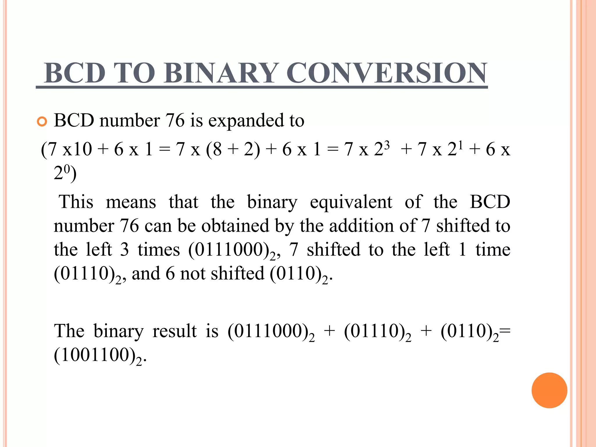
Downloaded 30 times
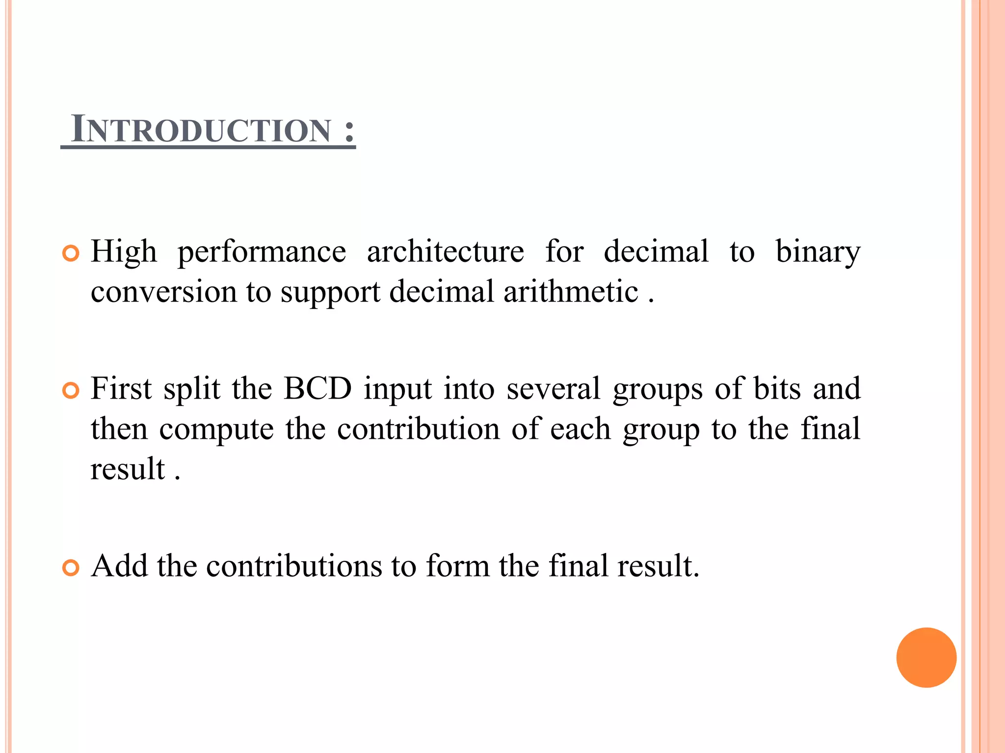

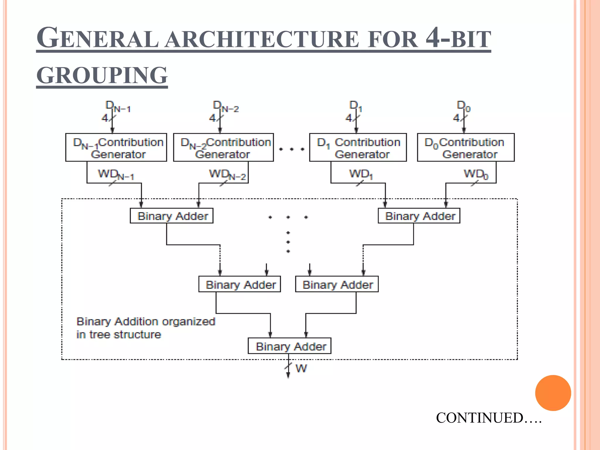
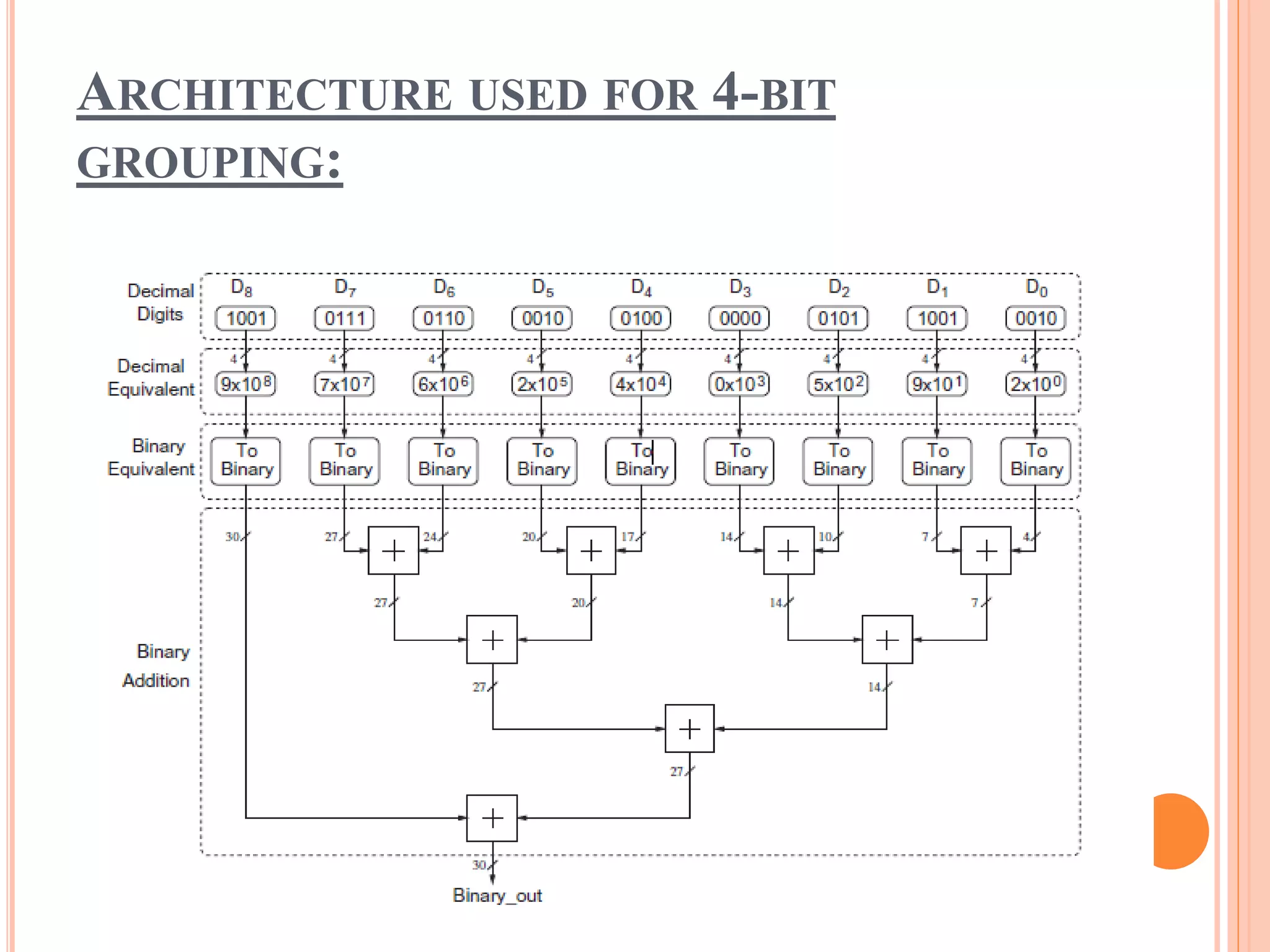
![HOW TO CALCULATE SIZE OF WDI ?
Digit at position i contributes to the final binary result
with size WDi can be manually calculated as :
WDi = [log2 ( 9 x10i )]+ 1 bits; i = 0, 1, . . . N – 1,
and the final binary result w requires W bits where
W = [log2 (10N -1)]+ 1 bits.](https://image.slidesharecdn.com/pptondtb-150416053614-conversion-gate02/75/High-Performance-FPGA-Based-Decimal-to-Binary-Conversion-Schemes-14-2048.jpg)


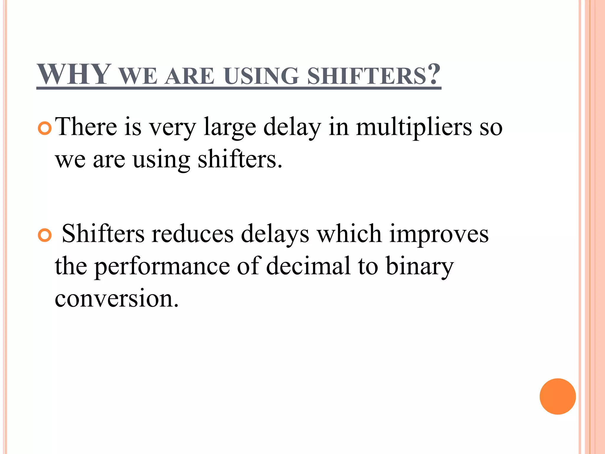
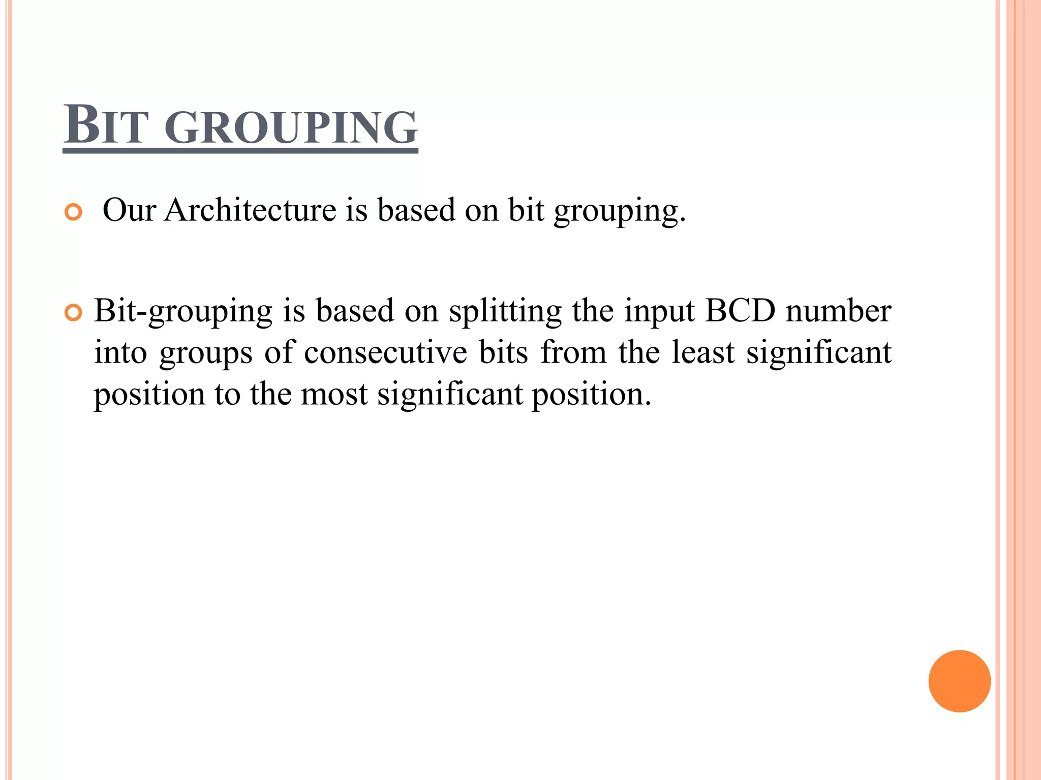
This document presents high-performance FPGA-based schemes for converting decimal to binary, employing bit-grouping techniques to enhance decimal arithmetic efficiency. It emphasizes the advantages of using shifters to reduce delays and improve performance in financial and scientific applications. The proposed architecture requires fewer look-up tables (LUTs) and demonstrates reduced delay compared to traditional methods.