unit -5-POWER AMPLIFIERS AND SPECIAL DEVICES (1).pdf
1.
P.SRIDHAR,AP/EEE,KONGUNADU COLLEGE OFENGINEERING AND
TECHNOLOGY, TRICHY.
5.1
KONGUNADU COLLEGE OF ENGINEERING AND TECHNOLOGY
(AUTONOMOUS)
NAMAKKAL-TRICHY MAIN ROAD, THOTTIAM, TRICHY -621 215
DEPARTMENT OF ELECTRICAL AND ELECTRONICS ENGINEERING
24EE302-ELECTRON DEVICES AND CIRCUITS
UNIT V
POWER AMPLIFIERS AND SPECIAL DEVICES
Power amplifiers:
The main aim of power amplifiers, otherwise called large signal amplifier is to deliver a
substantial amount of power to a load. A large signal amplifier must operate efficiently and
should be capable of handling power ranging from a few watts to few 100 watts. These
amplifiers are characterized by high efficiency, maximum power handling capacity and good
impedance matching.
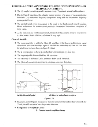
Class A Amplifiers
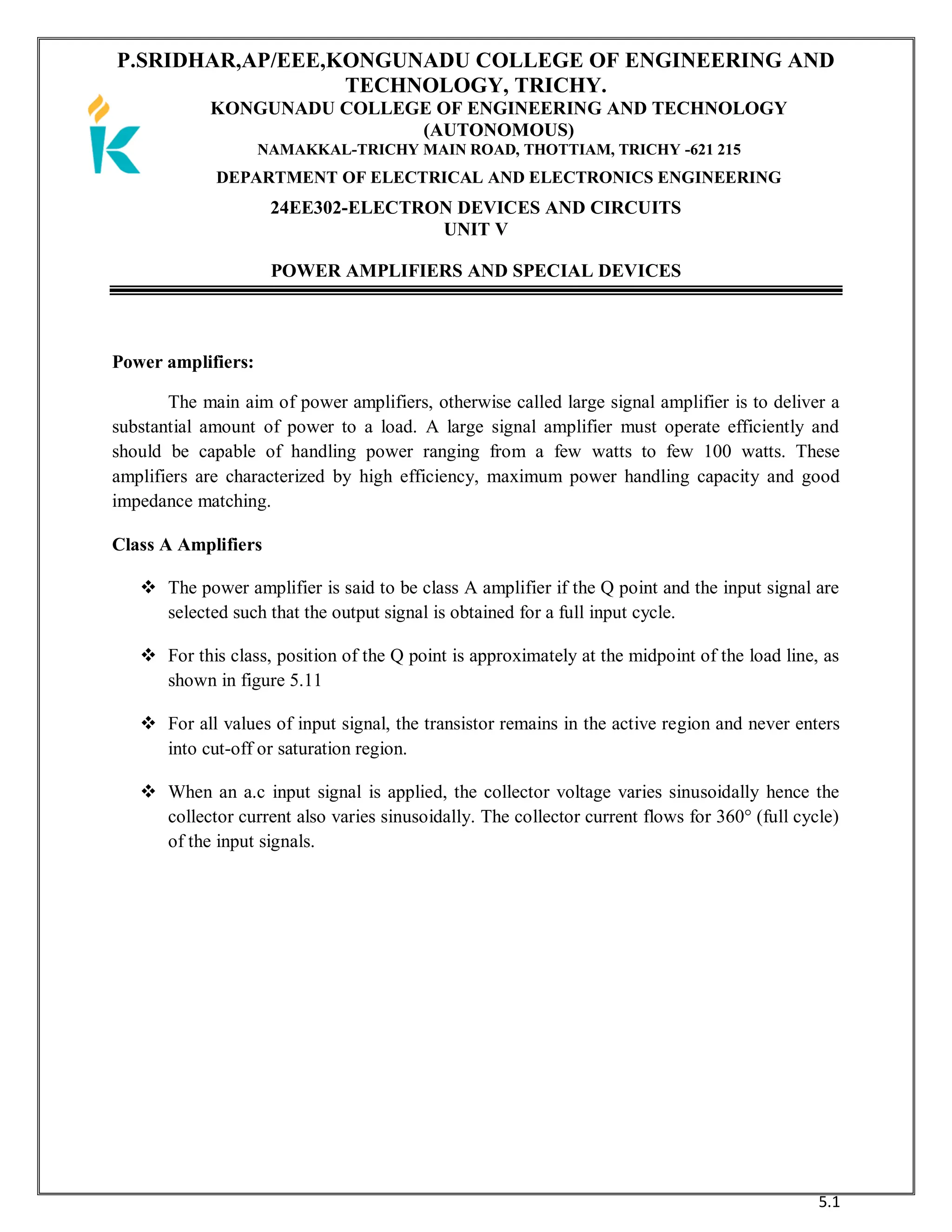
The power amplifier is said to be class A amplifier if the Q point and the input signal are
selected such that the output signal is obtained for a full input cycle.
For this class, position of the Q point is approximately at the midpoint of the load line, as
shown in figure 5.11
For all values of input signal, the transistor remains in the active region and never enters
into cut-off or saturation region.
When an a.c input signal is applied, the collector voltage varies sinusoidally hence the
collector current also varies sinusoidally. The collector current flows for 360° (full cycle)
of the input signals.
2.
P.SRIDHAR,AP/EEE,KONGUNADU COLLEGE OFENGINEERING AND
TECHNOLOGY, TRICHY.
5.2
Figure 5.11 Position of Q-point for Class A amplifier
For Class A amplifier, for full input cycle, a full output cycle is obtained. Here signal is
faithfully reproduced at the output without any distortion.
The efficiency of Class A operation is very small.
Figure 5.12 Current and voltage waveforms
Class B Amplifier
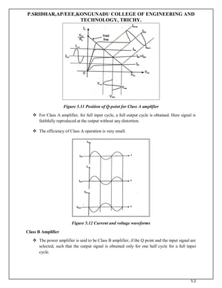
The power amplifier is said to be Class B amplifier, if the Q point and the input signal are
selected, such that the output signal is obtained only for one half cycle for a full input
cycle.
3.
P.SRIDHAR,AP/EEE,KONGUNADU COLLEGE OFENGINEERING AND
TECHNOLOGY, TRICHY.
5.3
For this operation, the Q point is shifted on X-axis i.e., transistor is biased to cut-off as
shown in figure 5.13.
(a) Position of Q-point (b) Current and voltage waveform
Due to the selection of Q point on the X-axis, the transistor remains in the active region,
only for positive half cycle of the input signal. Hence this half cycle is reproduced at the
output.
But in a negative half cycle of the input signal, the transistor enters into a cut-off region
and no signal is produced at the output.
The collector current flows only for 180° (half cycle) of the input signals.
As only a half cycle is obtained at the output, for full input cycle, the output signal is
distorted in this mode of operation.
To eliminate this distortion, practically two transistors are used in the alternate half cycles
of the input signal. Thus, overall a full cycle of output signal is obtained across the load.
Each transistor conducts only for a half cycle of the input signal.
The efficiency of Class B operation is much higher than the Class A operation.
Class C Amplifiers:
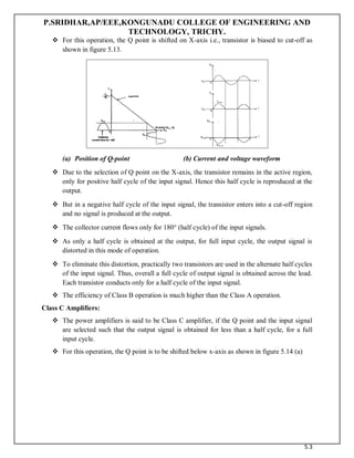
The power amplifiers is said to be Class C amplifier, if the Q point and the input signal
are selected such that the output signal is obtained for less than a half cycle, for a full
input cycle.
For this operation, the Q point is to be shifted below x-axis as shown in figure 5.14 (a)
4.
P.SRIDHAR,AP/EEE,KONGUNADU COLLEGE OFENGINEERING AND
TECHNOLOGY, TRICHY.
5.4
(a) Position of Q-point (b) Current and voltage waveform
Due to such a selection of the Q point, transistor remains active, for less than a half cycle.
Hence only that much part is reproduced at the output.
For remaining cycle of the input cycle, the transistor remains cut-off and no signal is
produced at the output. The collector current flow is less than 180°
As the collector current flows for less than 180°, the output is much more distorted and
hence the Class C mode is never used for A.F power amplifiers.
The efficiency of this class of operation is much higher and can reach very close to
100%.
Applications: The Class C operation is not suitable for audio frequency power amplifiers. The
Class C amplifiers are used in tuned circuits used in communication areas and in ratio frequency
(RF) amplifiers. These are also used in mixer or converter circuits used in radio receivers and
wireless communication systems.
Class C tuned amplifier:
Class C tuned amplifier
5.
P.SRIDHAR,AP/EEE,KONGUNADU COLLEGE OFENGINEERING AND
TECHNOLOGY, TRICHY.
5.5
The LC parallel circuit is a parallel resonant circuit. This circuit acts as load impedance.
Due to Class C operation, the collector current consists of a series of pulses containing
harmonics (i.e) many other frequency components along with the fundamental frequency
component of input.
The parallel tuned circuit is designed to be tuned to the fundamental input frequency.
Hence it eliminates the harmonics and produce a sinewave of fundamental component of
input signal.
As the transistor and coil losses are small, the most of the d.c input power is converted to
a.c load power. Hence efficiency of class C is very high.
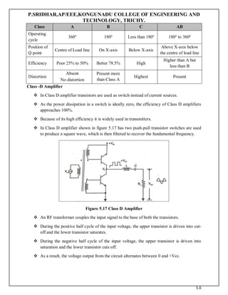
Class AB Amplifier
The power amplifier is said to be Class AB amplifier, if the Q point and the input signal
are selected such that the output signal is obtained for more than 180o
but less than 360°
for a full input cycle as shown in figure 5.160(a).
The Q point position is above X-axis but below the midpoint of a load line.
The output signal is distorted in Class AB operation.
The efficiency is more than Class A but less than Class B operation.
The Class AB operation is important to eliminate cross over distortion.
(a) Position of Q-point (b) Current and voltage waveform
Figure 5.16
In general, as the Q point moves away from the center of the loadline below towards the
X-axis, the efficiency of Class of operation increases.
Comparison of Amplifier Classes
Comaprison of amplifier classes
6.
P.SRIDHAR,AP/EEE,KONGUNADU COLLEGE OFENGINEERING AND
TECHNOLOGY, TRICHY.
5.6
Class A B C AB
Operating
cycle
360o
180o
Less than 180o
180o
to 360o
Position of
Q point
Centre of Load line On X-axis Below X-axis
Above X-axis below
the centre of load line
Efficiency Poor 25% to 50% Better 78.5% High
Higher than A but
less than B
Distortion
Absent
No distortion
Present more
than Class A
Highest Present
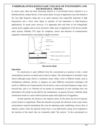
Class -D Amplifier
In Class D amplifier transistors are used as switch instead of current sources.
As the power dissipation in a switch is ideally zero, the efficiency of Class D amplifiers
approaches 100%.
Because of its high efficiency it is widely used in transmitters.
In Class D amplifier shown in figure 5.17 has two push-pull transistor switches are used
to produce a square wave, which is then filtered to recover the fundamental frequency.
Figure 5.17 Class D Amplifier
An RF transformer couples the input signal to the base of both the transistors.
During the positive half cycle of the input voltage, the upper transistor is driven into cut-
off and the lower transistor saturates.
During the negative half cycle of the input voltage, the upper transistor is driven into
saturation and the lower transistor cuts off.
As a result, the voltage output from the circuit alternates between 0 and +Vcc.
7.
P.SRIDHAR,AP/EEE,KONGUNADU COLLEGE OFENGINEERING AND
TECHNOLOGY, TRICHY.
5.7
This square wave is given as input to a high Q series resonance circuit which transmit the
fundamental frequency alone while blocking the harmonics.
The square wave at the output of push-pull amplifier can be expressed as
𝑉
𝑐 = 0.636𝑉
𝑐𝑐 [𝑠𝑖𝑛𝜃 +
𝑠𝑖𝑛3𝜃
3
+
𝑠𝑖𝑛5𝜃
5
+ ⋯ ] ---------------------- (5.30)
The voltage output from the circuit is almost a sine wave is given by
𝑉𝑜𝑢𝑡 = 0.636𝑉
𝑐𝑐 𝑠𝑖𝑛𝜃
Thus, the maximum value of the output sinewave is 0.636 Vcc.
Class S Amplifier
Class S operation of a transistor is mostly used in switching regulators.
Figure 5.18 Class S Amplifier
A continuous string of pulses of an amplitude Vccdruves the transistor in emitter
followers connection.
Because of the VBE drop, the voltage driving the LC filter is a train of pulses with an
amplitude of Vcc- VBE.
If XL, is much greater than Xc at the switching frequency, the output is a d.c voltage of
Vdc=D(VCC-VBE)
Where D is the duty cycle of the input waveform. Thus, higher the duty cycle larger will
be the d.c output.
The switching regulator uses a Class S amplifier in which by varying the duty cycle we
can regulate the d.c output.
Since the transistor is switched into either cut-off or saturation its power dissipation is
much lower.
SCHOTTKY DIODE: (HOT-CARRIER)
Construction:
8.
P.SRIDHAR,AP/EEE,KONGUNADU COLLEGE OFENGINEERING AND
TECHNOLOGY, TRICHY.
5.8
In recent years, there has been increasing interest in a two-terminal device referred to as a
Schottky-barrier, surface-barrier, or hot-carrier diode. Its areas of application were first limited to
the very high frequency range due to its quick response time (especially important at high
frequencies) and a lower noise figure (a quantity of real importance in high-frequency
applications). In recent years, however, it is appearing more and more in low-voltage/high-
current power supplies and ac-to-dc converters. Other areas of application of the device include
radar systems, Schottky TTL logic for computers, mixers and detectors in communication
equipment, instrumentation, and analog-to-digital converters.
Hot-carrier diode
Operation:
Its construction is quite different from the conventional p-n junction in that a metal
semiconductor junction is created such as shown in figure. The semiconductor is normally n-type
silicon (although p-type silicon is sometimes used), whiles a host of different metals, such as
molybdenum, platinum, chrome, or tungsten, are used. Different construction techniques will
result in a different set of characteristics for the device, such as increased frequency range, lower
forward bias, and so on. Priorities do not permit an examination of each technique here, but
information will usually be provided by the manufacturer. In general, however, Schottky diode
construction results in a more uniform junction region and a high level of ruggedness.
In both materials, the electron is the majority carrier. In the metal, the level of minority
carriers (holes) is insignificant. When the materials are joined, the electrons in the n-type silicon
semiconductor material immediately flow into the adjoining metal, establishing a heavy flow of
majority carriers. Since the injected carriers have a very high kinetic energy level compared to
the electrons of the metal, they are commonly called “hot carriers.” In the conventional p-n
9.
P.SRIDHAR,AP/EEE,KONGUNADU COLLEGE OFENGINEERING AND
TECHNOLOGY, TRICHY.
5.9
junction, there was the injection of minority carriers into the adjoining region. Here the electrons
are injected into a region of the same electron plurality.
Characteristics:
Comparison of characteristics of hot-carrier and p-n junction diodes
The application of a forward bias as shown in the first quadrant of figure. Will reduce the
strength of the negative barrier through the attraction of the applied positive potential for
electrons from this region. The result is a return to the heavy flow of electrons across the
boundary, the magnitude of which is controlled by the level of the applied bias potential. The
barrier at the junction for a Schottky diode is less than that of the p-n junction device in both the
forward- and reverse-bias regions. The result is therefore a higher current at the same applied
bias in the forward- and reverse-bias regions. This is a desirable effect in the forward-bias region
but highly undesirable in the reverse-bias region.
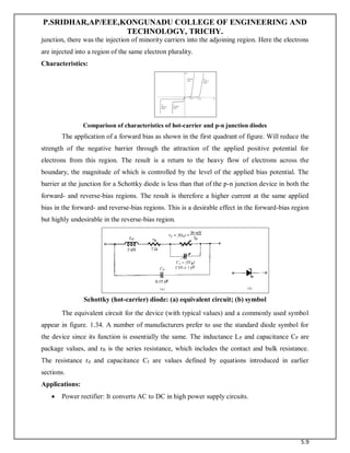
Schottky (hot-carrier) diode: (a) equivalent circuit; (b) symbol
The equivalent circuit for the device (with typical values) and a commonly used symbol
appear in figure. 1.34. A number of manufacturers prefer to use the standard diode symbol for
the device since its function is essentially the same. The inductance LP and capacitance CP are
package values, and rB is the series resistance, which includes the contact and bulk resistance.
The resistance rd and capacitance CJ are values defined by equations introduced in earlier
sections.
Applications:
Power rectifier: It converts AC to DC in high power supply circuits.
10.
P.SRIDHAR,AP/EEE,KONGUNADU COLLEGE OFENGINEERING AND
TECHNOLOGY, TRICHY.
5.10
Reverse current protection: It prevents the flow of current in the opposite direction.
Discharge protection: It protects the circuit from overvoltage or over current.
Voltage clamping: It limits the voltage to a certain level.
RF mixer and detector: It combines or separates radio frequency signals.
Solar cell: It converts solar energy into electrical energy.
Logic gates, digital circuits, and memory devices: It performs binary operations and data
storage.
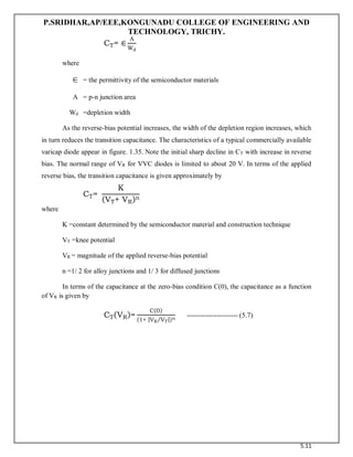
VARACTOR DIODE:(VARICAP)
Construction:
Varactor diode is a special type of diode which uses transition capacitance property i.e
voltage variable capacitance .These are also called as varicap, VVC (voltage variable
capacitance) or tuning diodes. The varactor diode symbol is shown below with a diagram
representation.
Varactor [also called varicap, VVC (voltage-variable capacitance), or tuning] diodes are
semiconductor, voltage-dependent, variable capacitors. Their mode of operation depends on the
capacitance that exists at the p-n junction when the element is reverse-biased. Under reverse-bias
conditions, it was established that there is a region of uncovered charge on either side of the
junction that together the regions make up the depletion region and define the depletion width
Wd. The transition capacitance (CT) established by the isolated uncovered charges is determined
by
Symbol
Structure of varactor diode
11.
P.SRIDHAR,AP/EEE,KONGUNADU COLLEGE OFENGINEERING AND
TECHNOLOGY, TRICHY.
5.11
CT= ∈
A
Wd
where
= the permittivity of the semiconductor materials
A = p-n junction area
Wd =depletion width
As the reverse-bias potential increases, the width of the depletion region increases, which
in turn reduces the transition capacitance. The characteristics of a typical commercially available
varicap diode appear in figure. 1.35. Note the initial sharp decline in CT with increase in reverse
bias. The normal range of VR for VVC diodes is limited to about 20 V. In terms of the applied
reverse bias, the transition capacitance is given approximately by
CT=
K
(VT+ VR)n
where
K =constant determined by the semiconductor material and construction technique
VT =knee potential
VR = magnitude of the applied reverse-bias potential
n =1/ 2 for alloy junctions and 1/ 3 for diffused junctions
In terms of the capacitance at the zero-bias condition C(0), the capacitance as a function
of VR is given by
CT(VR)=
C(0)
(1+ |VR VT
⁄ |)n
---------------------- (5.7)
12.
P.SRIDHAR,AP/EEE,KONGUNADU COLLEGE OFENGINEERING AND
TECHNOLOGY, TRICHY.
5.12
Varicap characteristics: C (pF) versus VR
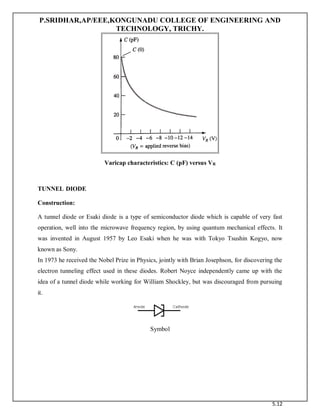
TUNNEL DIODE
Construction:
A tunnel diode or Esaki diode is a type of semiconductor diode which is capable of very fast
operation, well into the microwave frequency region, by using quantum mechanical effects. It
was invented in August 1957 by Leo Esaki when he was with Tokyo Tsushin Kogyo, now
known as Sony.
In 1973 he received the Nobel Prize in Physics, jointly with Brian Josephson, for discovering the
electron tunneling effect used in these diodes. Robert Noyce independently came up with the
idea of a tunnel diode while working for William Shockley, but was discouraged from pursuing
it.
Symbol
13.
P.SRIDHAR,AP/EEE,KONGUNADU COLLEGE OFENGINEERING AND
TECHNOLOGY, TRICHY.
5.13
Figure 5.20: Tunnel diode symbol and Construction
Working:
These diodes have a heavily doped p–n junction only some 10 nm (100 Å) wide. The heavy
doping results in a broken band gap, where conduction band electron states on the n-side are
more or less aligned with valence band hole states on the p-side. Tunnel diodes were
manufactured by Sony for the first time in 1957 followed by General Electric and other
companies from about 1960, and are still made in low volume today. Tunnel diodes are usually
made from germanium, but can also be made in gallium arsenide and silicon materials. They can
be used as oscillators, amplifiers, frequency converters and detectors.
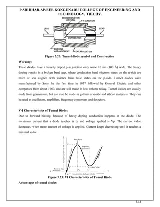
V-I Characteristics of Tunnel Diode:
Due to forward biasing, because of heavy doping conduction happens in the diode. The
maximum current that a diode reaches is Ip and voltage applied is Vp. The current value
decreases, when more amount of voltage is applied. Current keeps decreasing until it reaches a
minimal value.
Figure 5.23: VI Characteristics of Tunnel Diode
Advantages of tunnel diodes:
14.
P.SRIDHAR,AP/EEE,KONGUNADU COLLEGE OFENGINEERING AND
TECHNOLOGY, TRICHY.
5.14
Environmental immunity i.e. peak point is not a function of temperature.
Low cost and Low noise.
Low power consumption.
High speed i.e. tunneling takes place very fast at the speed of light in the order of
nanoseconds.
Simplicity i.e. a tunnel diode can be used along with a d.c supply and a few passive
elements to obtain various application circuits.
Applications for tunnel diodes:
Local oscillators for UHF television tuners.
Trigger circuits in oscilloscopes
High speed counter circuits and very fast-rise time pulse generator circuits
The tunnel diode can also be used as low-noise microwave amplifier.
OPTOCOUPLERS
Definition: An optocoupler or optoelectronic coupler is an electronic component that basically
acts as an interface between the two separate circuits with different voltage levels. Optocouplers
are common component by which electrical isolation can be supplied between the input and
output source. It is a 6 pin device and can have any number of photo detectors.
Here, a beam of light emitted by a light source exists as an only contact between input and
output. Due to this, we can have an insulation resistance of megaohms between the two circuits.
In high voltage applications where the voltage difference between the two circuits differs by
several thousand volts, such isolation is favourable. The use of all such electronic isolators lies in
all that conditions where the signal is to pass between two isolated circuits.
Construction of an Optocoupler:
An optocoupler mainly consists of an infrared LED and a photosensitive device that detects the
emitted infrared beam. The semiconductor photosensitive device can be a photodiode,
phototransistor, a Darlington pair, SCR or TRIAC.Let’s have a look at the basic diagram of an
Optocoupler:
The infrared LED and the device that is light sensitive is packed in a single package. The LED is
kept on the input side and the light-sensitive material is placed on the output side. A resistance is
15.
P.SRIDHAR,AP/EEE,KONGUNADU COLLEGE OFENGINEERING AND
TECHNOLOGY, TRICHY.
5.15
connected at the beginning of the circuit which is used to limit the current and the other
resistance is connected between the supply voltage and the collector terminal.
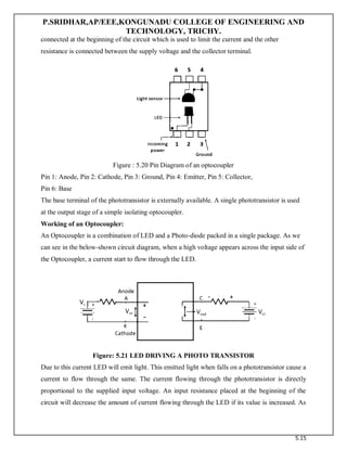
Figure : 5.20 Pin Diagram of an optocoupler
Pin 1: Anode, Pin 2: Cathode, Pin 3: Ground, Pin 4: Emitter, Pin 5: Collector,
Pin 6: Base
The base terminal of the phototransistor is externally available. A single phototransistor is used
at the output stage of a simple isolating optocoupler.
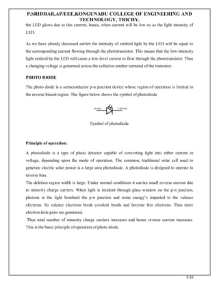
Working of an Optocoupler:
An Optocoupler is a combination of LED and a Photo-diode packed in a single package. As we
can see in the below-shown circuit diagram, when a high voltage appears across the input side of
the Optocoupler, a current start to flow through the LED.
Figure: 5.21 LED DRIVING A PHOTO TRANSISTOR
Due to this current LED will emit light. This emitted light when falls on a phototransistor cause a
current to flow through the same. The current flowing through the phototransistor is directly
proportional to the supplied input voltage. An input resistance placed at the beginning of the
circuit will decrease the amount of current flowing through the LED if its value is increased. As
16.
P.SRIDHAR,AP/EEE,KONGUNADU COLLEGE OFENGINEERING AND
TECHNOLOGY, TRICHY.
5.16
the LED glows due to this current, hence, when current will be low so as the light intensity of
LED.
As we have already discussed earlier the intensity of emitted light by the LED will be equal to
the corresponding current flowing through the phototransistor. This means that the low-intensity
light emitted by the LED will cause a low-level current to flow through the phototransistor. Thus
a changing voltage is generated across the collector-emitter terminal of the transistor.
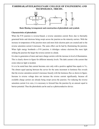
PHOTO DIODE
The photo diode is a semiconductor p-n junction device whose region of operation is limited to
the reverse biased region. The figure below shows the symbol of photodiode
Symbol of photodiode
Principle of operation:
A photodiode is a type of photo detector capable of converting light into either current or
voltage, depending upon the mode of operation. The common, traditional solar cell used to
generate electric solar power is a large area photodiode. A photodiode is designed to operate in
reverse bias.
The deletion region width is large. Under normal conditions it carries small reverse current due
to minority charge carriers. When light is incident through glass window on the p-n junction,
photons in the light bombard the p-n junction and some energy’s imparted to the valence
electrons. So valence electrons break covalent bonds and become free electrons. Thus more
electron-hole pairs are generated.
Thus total number of minority charge carriers increases and hence reverse current increases.
This is the basic principle of operation of photo diode.
17.
P.SRIDHAR,AP/EEE,KONGUNADU COLLEGE OFENGINEERING AND
TECHNOLOGY, TRICHY.
5.17
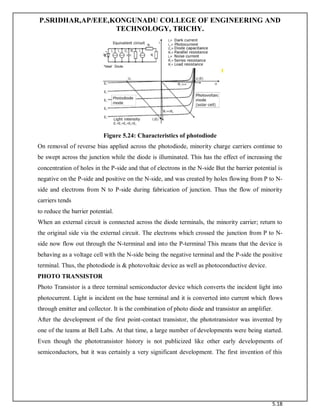
Basic Biasing Arrangement and construction of photodiode and symbols
Characteristics of photodiode:
When the P-N junction is reverse-biased, a reverse saturation current flows due to thermally
generated holes and electrons being swept across the junction as the minority carriers. With the
increase in temperature of the junction more and more hole-electron pairs are created and so the
reverse saturation current I0 increases. The same effect can be had by illuminating the junction.
When light energy bombards a P-N junction, it dislodges valence electrons.The more light
striking the junction the larger the reverse current in a diode.
It is due to generation of more and more charge carriers with the increase in level of illumination.
This is clearly shown in figure for different intensity levels. The dark current is the current that
exists when no light is incident.
It is to be noted here that current becomes zero only with a positive applied bias equals to VQ.
The almost equal spacing between the curves for the same increment in luminous flux reveals
that the reverse saturation current I0 increases linearly with the luminous flux as shown in figure.
Increase in reverse voltage does not increase the reverse current significantly, because all
available charge carriers are already being swept across the junction. For reducing the reverse
saturation current I0 to zero, it is necessary to forward bias the junction by an amount equal to
barrier potential. Thus the photodiode can be used as a photoconductive device.
18.
P.SRIDHAR,AP/EEE,KONGUNADU COLLEGE OFENGINEERING AND
TECHNOLOGY, TRICHY.
5.18
Figure 5.24: Characteristics of photodiode
On removal of reverse bias applied across the photodiode, minority charge carriers continue to
be swept across the junction while the diode is illuminated. This has the effect of increasing the
concentration of holes in the P-side and that of electrons in the N-side But the barrier potential is
negative on the P-side and positive on the N-side, and was created by holes flowing from P to N-
side and electrons from N to P-side during fabrication of junction. Thus the flow of minority
carriers tends
to reduce the barrier potential.
When an external circuit is connected across the diode terminals, the minority carrier; return to
the original side via the external circuit. The electrons which crossed the junction from P to N-
side now flow out through the N-terminal and into the P-terminal This means that the device is
behaving as a voltage cell with the N-side being the negative terminal and the P-side the positive
terminal. Thus, the photodiode is & photovoltaic device as well as photoconductive device.
PHOTO TRANSISTOR
Photo Transistor is a three terminal semiconductor device which converts the incident light into
photocurrent. Light is incident on the base terminal and it is converted into current which flows
through emitter and collector. It is the combination of photo diode and transistor an amplifier.
After the development of the first point-contact transistor, the phototransistor was invented by
one of the teams at Bell Labs. At that time, a large number of developments were being started.
Even though the phototransistor history is not publicized like other early developments of
semiconductors, but it was certainly a very significant development. The first invention of this
19.
P.SRIDHAR,AP/EEE,KONGUNADU COLLEGE OFENGINEERING AND
TECHNOLOGY, TRICHY.
5.19
transistor was announced on March 30th, 1950. This article discusses an overview of a
phototransistor and its working.
A semiconductor device like a phototransistor includes three layers with a light-sensitive base
region. Here, the base region detects the light & changes it into the current that supplies among
the two regions like the emitter & the collector.
Alternatively, a phototransistor is also considered like a Photodiode including a current
amplifier. This transistor changes directly from photons to charge similar to a photodiode and
also offers a current gain. The phototransistor symbol is shown below that is the same as an
ordinary transistor but the main difference is that the two arrows on this will explain the light
incident on the base terminal of the transistor.
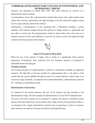
Figure:5.25 Symbol of Photo Diode
When the size of the junction is higher, then it results in a significantly better junction
capacitance. Consequently, these transistors have less frequency response as compared to
photodiode despite the high gain.
Working Principle:
The working principle of a phototransistor is similar to a photodiode including an amplifying
transistor. The light falls on the base terminal of a phototransistor then it will induce a little
current then the current amplified through the action of a normal transistor, which results in an
extensively large. Generally, as compared with a related photodiode, a phototransistor generates
50 – 100 times of a photodiode current.
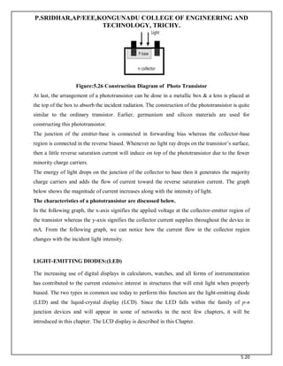
Phototransistor Construction:
As compared to the normal transistor, the area of the collector and base terminals in the
phototransistor is large. The best example of a phototransistor IC is the 2N5777 phototransistor.
The area of the base terminal can be increased to enhance the amount of produced current
because when more light drops on this transistor then a huge current will be generated. Before, it
was designed with a single semiconductor material such as germanium or silicon. At present,
these transistors are made up of Arsenic & Gallium to get high efficiency.
20.
P.SRIDHAR,AP/EEE,KONGUNADU COLLEGE OFENGINEERING AND
TECHNOLOGY, TRICHY.
5.20
Figure:5.26 Construction Diagram of Photo Transistor
At last, the arrangement of a phototransistor can be done in a metallic box & a lens is placed at
the top of the box to absorb the incident radiation. The construction of the phototransistor is quite
similar to the ordinary transistor. Earlier, germanium and silicon materials are used for
constructing this phototransistor.
The junction of the emitter-base is connected in forwarding bias whereas the collector-base
region is connected in the reverse biased. Whenever no light ray drops on the transistor’s surface,
then a little reverse saturation current will induce on top of the phototransistor due to the fewer
minority charge carriers.
The energy of light drops on the junction of the collector to base then it generates the majority
charge carriers and adds the flow of current toward the reverse saturation current. The graph
below shows the magnitude of current increases along with the intensity of light.
The characteristics of a phototransistor are discussed below.
In the following graph, the x-axis signifies the applied voltage at the collector-emitter region of
the transistor whereas the y-axis signifies the collector current supplies throughout the device in
mA. From the following graph, we can notice how the current flow in the collector region
changes with the incident light intensity.
LIGHT-EMITTING DIODES:(LED)
The increasing use of digital displays in calculators, watches, and all forms of instrumentation
has contributed to the current extensive interest in structures that will emit light when properly
biased. The two types in common use today to perform this function are the light-emitting diode
(LED) and the liquid-crystal display (LCD). Since the LED falls within the family of p-n
junction devices and will appear in some of networks in the next few chapters, it will be
introduced in this chapter. The LCD display is described in this Chapter.
21.
P.SRIDHAR,AP/EEE,KONGUNADU COLLEGE OFENGINEERING AND
TECHNOLOGY, TRICHY.
5.21
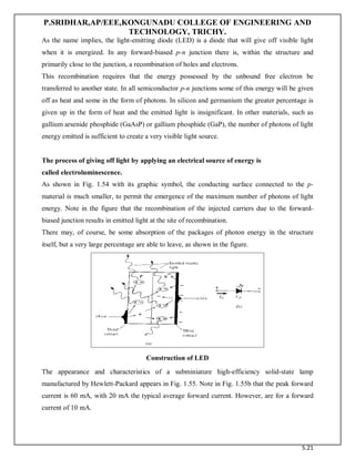
As the name implies, the light-emitting diode (LED) is a diode that will give off visible light
when it is energized. In any forward-biased p-n junction there is, within the structure and
primarily close to the junction, a recombination of holes and electrons.
This recombination requires that the energy possessed by the unbound free electron be
transferred to another state. In all semiconductor p-n junctions some of this energy will be given
off as heat and some in the form of photons. In silicon and germanium the greater percentage is
given up in the form of heat and the emitted light is insignificant. In other materials, such as
gallium arsenide phosphide (GaAsP) or gallium phosphide (GaP), the number of photons of light
energy emitted is sufficient to create a very visible light source.
The process of giving off light by applying an electrical source of energy is
called electroluminescence.
As shown in Fig. 1.54 with its graphic symbol, the conducting surface connected to the p-
material is much smaller, to permit the emergence of the maximum number of photons of light
energy. Note in the figure that the recombination of the injected carriers due to the forward-
biased junction results in emitted light at the site of recombination.
There may, of course, be some absorption of the packages of photon energy in the structure
itself, but a very large percentage are able to leave, as shown in the figure.
Construction of LED
The appearance and characteristics of a subminiature high-efficiency solid-state lamp
manufactured by Hewlett-Packard appears in Fig. 1.55. Note in Fig. 1.55b that the peak forward
current is 60 mA, with 20 mA the typical average forward current. However, are for a forward
current of 10 mA.
22.
P.SRIDHAR,AP/EEE,KONGUNADU COLLEGE OFENGINEERING AND
TECHNOLOGY, TRICHY.
5.22
The level of VD under forward-bias conditions is listed as VF and extends from 2.2
to 3 V. In other words, one can expect a typical operating current of about 10 mA at
2.5 V for good light emission.
Two quantities yet undefined appear under the heading Electrical/Optical Characteristics at TA _
25°C. They are the axial luminous intensity (IV) and the luminous efficacy (_v). Light intensity
is measured in candela. One candela emits a light flux of 4_ lumens and establishes an
illumination of 1 foot candle on a 1-ft2 area 1 ft from the light source. Even though this
description may not provide a clear understanding of the candela as a unit of measure, its level
can certainly be compared between similar devices.
The term efficacy is, by definition, a measure of the ability of a device to produce a desired
effect. For the LED this is the ratio of the number of lumens generated per applied watt of
electrical energy.
The relative efficiency is defined by the luminous intensity per unit current, as shown in The
relative intensity of each color versus wavelength appears in Since the LED is a p-n junction
device, it will have a forward-biased characteristic similar to the diode response curves. Note the
almost linear increase in relative luminous intensity with forward current 1.55h reveals that the
longer the pulse duration at a particular frequency, the lower the permitted peak current (after
you pass the break value of tp). Figure 1.55i simply reveals that the intensity is greater at 0° (or
head on) and the least at 90° (when you view the device from the side).
LIQUID-CRYSTAL DISPLAYS
The liquid-crystal display (LCD) has the distinct advantage of having a lower power requirement
than the LED. It is typically in the order of microwatts for the display, as compared to the same
order of milliwatts for LEDs. It does, however, require anexternal or internal light source and is
limited to a temperature range of about 0° to60°C. Lifetime is an area of concern because LCDs
can chemically degrade. The typesreceiving the major interest today are the field-effect and
dynamic-scattering units.
A liquid crystal is a material (normally organic for LCDs) that will flow like aliquid but whose
molecular structure has some properties normally associated withsolids. For the light-scattering
units, the greatest interest is in the nematic liquid crystal,having the crystal structure shown in
figure.
23.
P.SRIDHAR,AP/EEE,KONGUNADU COLLEGE OFENGINEERING AND
TECHNOLOGY, TRICHY.
5.23
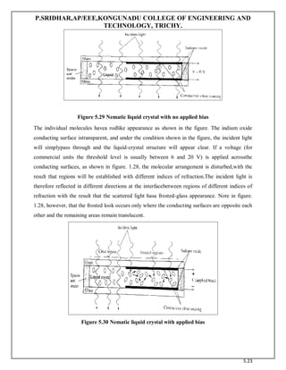
Figure 5.29 Nematic liquid crystal with no applied bias
The individual molecules havea rodlike appearance as shown in the figure. The indium oxide
conducting surface istransparent, and under the condition shown in the figure, the incident light
will simplypass through and the liquid-crystal structure will appear clear. If a voltage (for
commercial units the threshold level is usually between 6 and 20 V) is applied acrossthe
conducting surfaces, as shown in figure. 1.28, the molecular arrangement is disturbed,with the
result that regions will be established with different indices of refraction.The incident light is
therefore reflected in different directions at the interfacebetween regions of different indices of
refraction with the result that the scattered light hasa frosted-glass appearance. Note in figure.
1.28, however, that the frosted look occurs only where the conducting surfaces are opposite each
other and the remaining areas remain translucent.
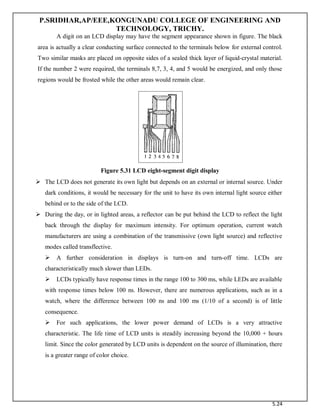
Figure 5.30 Nematic liquid crystal with applied bias
24.
P.SRIDHAR,AP/EEE,KONGUNADU COLLEGE OFENGINEERING AND
TECHNOLOGY, TRICHY.
5.24
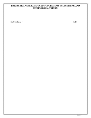
A digit on an LCD display may have the segment appearance shown in figure. The black
area is actually a clear conducting surface connected to the terminals below for external control.
Two similar masks are placed on opposite sides of a sealed thick layer of liquid-crystal material.
If the number 2 were required, the terminals 8,7, 3, 4, and 5 would be energized, and only those
regions would be frosted while the other areas would remain clear.
Figure 5.31 LCD eight-segment digit display
The LCD does not generate its own light but depends on an external or internal source. Under
dark conditions, it would be necessary for the unit to have its own internal light source either
behind or to the side of the LCD.
During the day, or in lighted areas, a reflector can be put behind the LCD to reflect the light
back through the display for maximum intensity. For optimum operation, current watch
manufacturers are using a combination of the transmissive (own light source) and reflective
modes called transflective.
A further consideration in displays is turn-on and turn-off time. LCDs are
characteristically much slower than LEDs.
LCDs typically have response times in the range 100 to 300 ms, while LEDs are available
with response times below 100 ns. However, there are numerous applications, such as in a
watch, where the difference between 100 ns and 100 ms (1/10 of a second) is of little
consequence.
For such applications, the lower power demand of LCDs is a very attractive
characteristic. The life time of LCD units is steadily increasing beyond the 10,000 + hours
limit. Since the color generated by LCD units is dependent on the source of illumination, there
is a greater range of color choice.

![P.SRIDHAR,AP/EEE,KONGUNADU COLLEGE OF ENGINEERING AND
TECHNOLOGY, TRICHY.
5.7
This square wave is given as input to a high Q series resonance circuit which transmit the
fundamental frequency alone while blocking the harmonics.
The square wave at the output of push-pull amplifier can be expressed as
𝑉
𝑐 = 0.636𝑉
𝑐𝑐 [𝑠𝑖𝑛𝜃 +
𝑠𝑖𝑛3𝜃
3
+
𝑠𝑖𝑛5𝜃
5
+ ⋯ ] ---------------------- (5.30)
The voltage output from the circuit is almost a sine wave is given by
𝑉𝑜𝑢𝑡 = 0.636𝑉
𝑐𝑐 𝑠𝑖𝑛𝜃
Thus, the maximum value of the output sinewave is 0.636 Vcc.
Class S Amplifier
Class S operation of a transistor is mostly used in switching regulators.
Figure 5.18 Class S Amplifier
A continuous string of pulses of an amplitude Vccdruves the transistor in emitter
followers connection.
Because of the VBE drop, the voltage driving the LC filter is a train of pulses with an
amplitude of Vcc- VBE.
If XL, is much greater than Xc at the switching frequency, the output is a d.c voltage of
Vdc=D(VCC-VBE)
Where D is the duty cycle of the input waveform. Thus, higher the duty cycle larger will
be the d.c output.
The switching regulator uses a Class S amplifier in which by varying the duty cycle we
can regulate the d.c output.
Since the transistor is switched into either cut-off or saturation its power dissipation is
much lower.
SCHOTTKY DIODE: (HOT-CARRIER)
Construction:](https://image.slidesharecdn.com/unit-5-poweramplifiersandspecialdevices1-250712161858-21c8b384/85/unit-5-POWER-AMPLIFIERS-AND-SPECIAL-DEVICES-1-pdf-7-320.jpg)
![P.SRIDHAR,AP/EEE,KONGUNADU COLLEGE OF ENGINEERING AND
TECHNOLOGY, TRICHY.
5.10
Reverse current protection: It prevents the flow of current in the opposite direction.
Discharge protection: It protects the circuit from overvoltage or over current.
Voltage clamping: It limits the voltage to a certain level.
RF mixer and detector: It combines or separates radio frequency signals.
Solar cell: It converts solar energy into electrical energy.
Logic gates, digital circuits, and memory devices: It performs binary operations and data
storage.
VARACTOR DIODE:(VARICAP)
Construction:
Varactor diode is a special type of diode which uses transition capacitance property i.e
voltage variable capacitance .These are also called as varicap, VVC (voltage variable
capacitance) or tuning diodes. The varactor diode symbol is shown below with a diagram
representation.
Varactor [also called varicap, VVC (voltage-variable capacitance), or tuning] diodes are
semiconductor, voltage-dependent, variable capacitors. Their mode of operation depends on the
capacitance that exists at the p-n junction when the element is reverse-biased. Under reverse-bias
conditions, it was established that there is a region of uncovered charge on either side of the
junction that together the regions make up the depletion region and define the depletion width
Wd. The transition capacitance (CT) established by the isolated uncovered charges is determined
by
Symbol
Structure of varactor diode](https://image.slidesharecdn.com/unit-5-poweramplifiersandspecialdevices1-250712161858-21c8b384/85/unit-5-POWER-AMPLIFIERS-AND-SPECIAL-DEVICES-1-pdf-10-320.jpg)


![RF Module Design - [Chapter 6] Power Amplifier](https://cdn.slidesharecdn.com/ss_thumbnails/rfch6-150613070347-lva1-app6891-thumbnail.jpg?width=640&height=640&fit=bounds)


