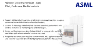
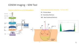
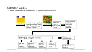
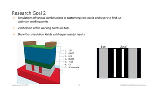
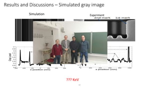
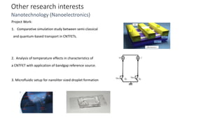
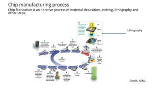
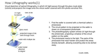
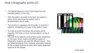
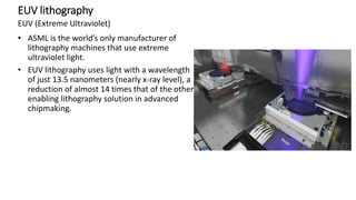
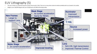
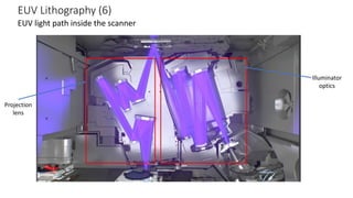
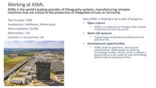
My semiconductor Journey
ASML in 1 minute
Introduction
Name: Shawn Millat
Currently living (From 2016) Origin (Born to 2011)
2011-2015
Education
BSc and MSc at Faculty of Engineering (2006 - 2011)
University of Chittagong
- BSc. Degree in Electronics and Communication Engineering
- Bachelor Project: Development of Students Online Information Sharing System
- MSc. Degree in Electronics and Communication Engineering
Master of Science at Faculty of Electrical Engineering and IT(2012 - 2015)
Central campus
Dresden University of Technology(founded in 1828)
Faculty of Electrical Engineering
and IT
- Master Degree in Nanoelectronic Systems
- Major: Semiconductor Technology
- Research Focus: CD and Overlay Metrology
- Main modules:
- Micro&nanoelectronics,
- Nanotechnology,
- Semiconductor process technology &
Integration
- Integrated Circuits
Prof. Johann Bartha
Chair holder of
Semiconductor
Technology,
TU Dresden
Profession
Process Development Traineeship Engineer (2013 - 2016)
GLOBALFOUNDRIES, Dresden, Germany
1. Providing support for the improvement of CD and Overlay measurement techniques
2. SPC, process monitoring and data analysis for CD and Overlay.
3. Report and presentation on CDSEM, KLA and Nanometrics tool data internally based on
customer requirements.
4. Macro development using Visual Basic Programming in Excel
Application Design Engineer (2016 - 2018)
ASML, Eindhoven, The Netherlands
1. Support ASML product integration by advice on metrology integration in process
patterning flow and identification of product budgets.
2. Analysis of metrology data to improve customer patterning performance and
yield via evaluation of monitoring and control strategies.
3. Design and Develop means & methods and WoW to assess, predict and drive
new ASML application product for customer use cases.
4. Cooperate in a constructive way with team members, R&D application experts
and customer support to drive fast and pragmatic solutions for the customers.
Customer Support Engineer (EUV Metrology and Sensors) (2018 - ongoing)
ASML, Eindhoven, The Netherlands
1. Perform analysis of structural issues of the systems at our customers.
2. Identify structural improvements to the design of ASML products and estimate
their impact on CS operation.
3. Identify structural improvements to the Service Mix and implement them globally
in CS.
4. Handshake and validate Service Mix that is supplied with new products and
functionalities by D&E.
5. Transfer and maintain all relevant knowledge to the CS field engineers.
Research and Development
Master thesis
 Motivation: With decreasing structure sizes in leading-edge semiconductor manufacturing
the demand for an improved overlay control grows, asking for a higher number of in-chip
targets. Accommodation of the latter is often difficult due to spatial constraints, so the
targets have to be much smaller than common targets for optical metrology requiring a
CD-SEM to measure them.
 My task: Use of the JMONSEL calculation package by simulating the energy dependence of
secondary and backscattered electron yields for some customer given structures, basically
reflecting all use cases of CD-SEM overlay. Calculation results are confirmed with
respective working points and like structures on the Applied Materials Verity 5i CD-SEM
tool.
SEM Based Overlay – development of dedicated workflow using new imaging
capability on CD-SEM for inline process control within semiconductor
manufacturing environment. *
* 16TH EUROPEAN ADVANCED PROCESS CONTROL AND MANUFACTURING (APC|M) CONFERENCE Reutlingen (Stuttgart), GERMANY • April 11 – 13, 2016.
http://www.apcm-europe.eu/conference/agenda/
12
CDSEM Imaging – SEM Tool
12
Electron collection on a CD-SEM platform Electron Beam-Specimen Interaction - The Onion effect
PE - Primary Beam
SE - Secondary Electrons
BSE - Back Scattered Electrons
~1nm
Research Goal 1
September 10, 2020 13 GLOBALFOUNDRIES Confidential
 Dedicated Workflow development to apply simulation method.
Research Goal 2
September 10, 2020 14 GLOBALFOUNDRIES Confidential
 Simulations of various combinations of customer given stacks and layers to find out
optimum working points
 Verification of the working points on tool
 Show that simulation Yields valid experimental results
Results and Discussions – Simulated gray image
15
??? KeV
Simulation Experiment
Other research interests
Nanotechnology (Nanoelectronics)
Project Work:
1. Comparative simulation study between semi-classical
and quantum-based transport in CNTFETs.
2. Analysis of temperature effects in characteristics of
a CNTFET with application of bandgap reference source.
3. Microfluidic setup for nanoliter sized droplet formation
Why did I choose to study in
Germany?
FIVE REASONS TO STUDY IN GERMANY
Germany is the fourth most popular destination among international students in the world. More than
thirteen percent of students at German universities in 2018 came from all over the world - just like you.
Germany is an attractive place to study and German university degrees are highly respected by employers
worldwide.
Credit: DAAD.DE
Where to find information to study in Germany.
https://www.myguide.de/en/
Story about Semiconductor
manufacturing
Silicon Wafers (1)
• Chips are made on silicon wafers
• Wafers look similar to the CD. Currently 8” wafers are used, and some
manufacturers use 12” wafers
• CD is about 4”, for comparison
Credit: Wikiwand
Silicon Wafers (2)
• In one 8” silicon wafer, 500 chips may be made
• Rectangular chips
• Wafers are processed in a batch of 25 (called “LOT”)
• Single wafer, batch, continuous processes
330 million transistors
in a RAM chip
©Intel
Credit: INTEL
Chip manufacturing process
Chip fabrication is an iterative process of material deposition, etching, lithography and
other steps.
Credit: ASML
Lithography
How Lithography works(1)
Visual depiction of optical lithography, in which UV light passes through the glass mask plate
(reticle) and projects the image onto the silicon wafer covered with thin photo-sensitive film.
Credit: ASML
1. First the wafer is covered with a chemical called a
photoresist.
2. The circuit pattern to be projected on the wafer is
drawn on a transparent photomask.
3. The photolithography system shines UV light through
the photomask, projecting a shadow of the circuit
pattern on the wafer.
4. The photoresist reacts to the light. The parts of the
photoresist that react harden and protect the areas
directly beneath, allowing everything else to be etched
away.
How Lithography works (2)
• The Reticle blueprint is four times larger than the
intended pattern on the chip.
• With the pattern encoded in the light, the system’s
optics shrink and focus the pattern onto a
photosensitive silicon wafer.
• This process is repeated until the wafer is covered in
patterns, completing one layer of the wafer’s chips.
• To make an entire microchip, this process will be
repeated 100 times or more, laying patterns on top of
patterns.
• The size of the features to be printed varies depending
on the layer, which means that different types of
lithography systems are used for different layers – from
our latest-generation EUV (extreme ultraviolet) systems
for the smallest features to older DUV (deep ultraviolet)
systems for the largest.
Credit: ASML
ASML EUV Lithography
EUV lithography
• ASML is the world’s only manufacturer of
lithography machines that use extreme
ultraviolet light.
• EUV lithography uses light with a wavelength
of just 13.5 nanometers (nearly x-ray level), a
reduction of almost 14 times that of the other
enabling lithography solution in advanced
chipmaking.
EUV (Extreme Ultraviolet)
EUV Lithography (2)
• We want to make chips smaller and
cheaper
• EUV: extreme ultraviolet light; very short
wavelength
• We want the patterns on the wafer (CD)
as small as possible.
• Making NA bigger is too difficult and
expensive, so we make λ smaller
• Wavelength EUV: λ = 13.5 nm (λ NXT is
193 nm)
Why EUV??
NA
kCD

 1
CD: critical dimension, width of lines on the wafer
NA: numerical aperture, related to θ and thus the size of the lens
k1 factor: a measure for how ‘easy’ imaging is
The minimum feature size that a projection system can
print is given approximately by
EUV Lithography (3)
EUV in spectrum
EUV
13.5nm
, λ
EUV Lithography (4)
• EUV wavelength is 13.5nm hence a tiny extreme Ultraviolet which can absorb
by everything including glass lenses, the transparent quartz that the mask is
made of even by Air.
• All the above has to happen in Vacuum otherwise this 13.5nm light can absorb
by air.
• Hence, instead of transferring EUV through mask, the EUV masks are reflective.
And use mirrors to bounce the light on silicon wafer.
• A laser is producing at source is vaporizing a Tin (Tn) droplet (30u) to produce
EUV.
• The laser has 30KW power (15X stronger which cuts the steel) and hitting Tn with
50KHz frequency (50X/sec).
• This vaporized Tn droplet will absorb the energy and create a plasma .
• The electrons in the Tin absorb this plasma energy and when the return to the
rest they discharge some of the energy as EUV photons.
Some facts about EUV
https://www.youtube.com/watch?v=NHSR6AHNiDs
EUV Lithography (5)
• The size is similar to a school bus (only the scanner+Source parts in fab). There are so many others external modules available which are situated in the subfab.
• Weight is over 180,000 Kilogram with over 100,000 parts and 3000 interlockings cables.
EUV Lithography (6)
EUV light path inside the scanner
Illuminator
optics
Projection
lens
Working at ASML
Year founded: 1984
Headquarter: Veldhoven, Netherlands
Total employees: 24,900
Nationalities: 118
Locations in 16 countries: 60
ASML is the world's leading provider of lithography systems, manufacturing complex
machines that are critical to the production of integrated circuits or microchip
How ASML is helping to be a part of progress:
• Open culture
• ASML is a collective of thinkers and creative
mind from all over the world
• Work-Life balance
• A good balance between professional and
personal life.
• Development opportunities
• ASML built on openness, sharing and
collaboration. ASML keeps on pushing
technology further. Hence, there is always a
good chance to be a part of new technology
which helps to develop further.
Customer Support engineer
• 1st interface with Customers:
• For customers CS engineers are the face of the organization and the customers
voice back inside ASML.
• 1st to respond to issues.
• 1st to keep technological advancement on track.
• CS Engineers are on the front line of optimizing the next-generation technology
getting the systems installed, integrated, optimized, ramped up and maintained.
• CS engineering position is an adventure as much as a job with opportunities to
travel around the world where ASML customers are located.
As a customer support engineer :
Personal life
T
H
A
N
K
Y
O
U
Q&A
Backup
Overlay Metrology– Overlay Offset
40
Overlay measurement is the detection of alignment positioning of two or more
different structuring steps.
Target Pattern Pattern with Overlay
Offset Overlay Offset
Photo Ref. Wiki
= Centerline Position
Results – Imaging Schemes
41
Mx – Mx-1 CA-PC/RX Implant Resist layer
ASML:
1. EUV at INTEL: https://www.youtube.com/watch?v=oIiqVrKDtLc&t=303s
2. ASML Technologies: https://www.asml.com/en/technology
3. ASML youtube channel: https://www.youtube.com/user/ASMLcompany
4. ASML Products: https://www.asml.com/en/products
5. Career at ASML
6. ASML Foundation: https://www.asml.com/en/company/asml-foundation
GLOBALFOUNDRIES:
https://www.globalfoundries.com/
Study in Germany:
1. https://www.daad.de/en/
2. https://www.facebook.com/groups/BSAAG
Studying at TU DRESDEN:
1. TU Dresden: https://tu-dresden.de/
2. Nanoelectronic systems
Careers and lifestyle:
1. Germany: https://www.deutschland.de/en/career-education-and-lifestyle-in-germany
2. The Netherlands: https://www.careersinholland.com/

From APECE to ASML A Semiconductor Journey

  • 1.
  • 2.
    Introduction Name: Shawn Millat Currentlyliving (From 2016) Origin (Born to 2011) 2011-2015
  • 3.
  • 4.
    BSc and MScat Faculty of Engineering (2006 - 2011) University of Chittagong - BSc. Degree in Electronics and Communication Engineering - Bachelor Project: Development of Students Online Information Sharing System - MSc. Degree in Electronics and Communication Engineering
  • 5.
    Master of Scienceat Faculty of Electrical Engineering and IT(2012 - 2015) Central campus Dresden University of Technology(founded in 1828) Faculty of Electrical Engineering and IT - Master Degree in Nanoelectronic Systems - Major: Semiconductor Technology - Research Focus: CD and Overlay Metrology - Main modules: - Micro&nanoelectronics, - Nanotechnology, - Semiconductor process technology & Integration - Integrated Circuits Prof. Johann Bartha Chair holder of Semiconductor Technology, TU Dresden
  • 6.
  • 7.
    Process Development TraineeshipEngineer (2013 - 2016) GLOBALFOUNDRIES, Dresden, Germany 1. Providing support for the improvement of CD and Overlay measurement techniques 2. SPC, process monitoring and data analysis for CD and Overlay. 3. Report and presentation on CDSEM, KLA and Nanometrics tool data internally based on customer requirements. 4. Macro development using Visual Basic Programming in Excel
  • 8.
    Application Design Engineer(2016 - 2018) ASML, Eindhoven, The Netherlands 1. Support ASML product integration by advice on metrology integration in process patterning flow and identification of product budgets. 2. Analysis of metrology data to improve customer patterning performance and yield via evaluation of monitoring and control strategies. 3. Design and Develop means & methods and WoW to assess, predict and drive new ASML application product for customer use cases. 4. Cooperate in a constructive way with team members, R&D application experts and customer support to drive fast and pragmatic solutions for the customers.
  • 9.
    Customer Support Engineer(EUV Metrology and Sensors) (2018 - ongoing) ASML, Eindhoven, The Netherlands 1. Perform analysis of structural issues of the systems at our customers. 2. Identify structural improvements to the design of ASML products and estimate their impact on CS operation. 3. Identify structural improvements to the Service Mix and implement them globally in CS. 4. Handshake and validate Service Mix that is supplied with new products and functionalities by D&E. 5. Transfer and maintain all relevant knowledge to the CS field engineers.
  • 10.
  • 11.
    Master thesis  Motivation:With decreasing structure sizes in leading-edge semiconductor manufacturing the demand for an improved overlay control grows, asking for a higher number of in-chip targets. Accommodation of the latter is often difficult due to spatial constraints, so the targets have to be much smaller than common targets for optical metrology requiring a CD-SEM to measure them.  My task: Use of the JMONSEL calculation package by simulating the energy dependence of secondary and backscattered electron yields for some customer given structures, basically reflecting all use cases of CD-SEM overlay. Calculation results are confirmed with respective working points and like structures on the Applied Materials Verity 5i CD-SEM tool. SEM Based Overlay – development of dedicated workflow using new imaging capability on CD-SEM for inline process control within semiconductor manufacturing environment. * * 16TH EUROPEAN ADVANCED PROCESS CONTROL AND MANUFACTURING (APC|M) CONFERENCE Reutlingen (Stuttgart), GERMANY • April 11 – 13, 2016. http://www.apcm-europe.eu/conference/agenda/
  • 12.
    12 CDSEM Imaging –SEM Tool 12 Electron collection on a CD-SEM platform Electron Beam-Specimen Interaction - The Onion effect PE - Primary Beam SE - Secondary Electrons BSE - Back Scattered Electrons ~1nm
  • 13.
    Research Goal 1 September10, 2020 13 GLOBALFOUNDRIES Confidential  Dedicated Workflow development to apply simulation method.
  • 14.
    Research Goal 2 September10, 2020 14 GLOBALFOUNDRIES Confidential  Simulations of various combinations of customer given stacks and layers to find out optimum working points  Verification of the working points on tool  Show that simulation Yields valid experimental results
  • 15.
    Results and Discussions– Simulated gray image 15 ??? KeV Simulation Experiment
  • 16.
    Other research interests Nanotechnology(Nanoelectronics) Project Work: 1. Comparative simulation study between semi-classical and quantum-based transport in CNTFETs. 2. Analysis of temperature effects in characteristics of a CNTFET with application of bandgap reference source. 3. Microfluidic setup for nanoliter sized droplet formation
  • 17.
    Why did Ichoose to study in Germany?
  • 18.
    FIVE REASONS TOSTUDY IN GERMANY Germany is the fourth most popular destination among international students in the world. More than thirteen percent of students at German universities in 2018 came from all over the world - just like you. Germany is an attractive place to study and German university degrees are highly respected by employers worldwide. Credit: DAAD.DE
  • 19.
    Where to findinformation to study in Germany. https://www.myguide.de/en/
  • 20.
  • 21.
    Silicon Wafers (1) •Chips are made on silicon wafers • Wafers look similar to the CD. Currently 8” wafers are used, and some manufacturers use 12” wafers • CD is about 4”, for comparison Credit: Wikiwand
  • 22.
    Silicon Wafers (2) •In one 8” silicon wafer, 500 chips may be made • Rectangular chips • Wafers are processed in a batch of 25 (called “LOT”) • Single wafer, batch, continuous processes 330 million transistors in a RAM chip ©Intel Credit: INTEL
  • 23.
    Chip manufacturing process Chipfabrication is an iterative process of material deposition, etching, lithography and other steps. Credit: ASML Lithography
  • 24.
    How Lithography works(1) Visualdepiction of optical lithography, in which UV light passes through the glass mask plate (reticle) and projects the image onto the silicon wafer covered with thin photo-sensitive film. Credit: ASML 1. First the wafer is covered with a chemical called a photoresist. 2. The circuit pattern to be projected on the wafer is drawn on a transparent photomask. 3. The photolithography system shines UV light through the photomask, projecting a shadow of the circuit pattern on the wafer. 4. The photoresist reacts to the light. The parts of the photoresist that react harden and protect the areas directly beneath, allowing everything else to be etched away.
  • 25.
    How Lithography works(2) • The Reticle blueprint is four times larger than the intended pattern on the chip. • With the pattern encoded in the light, the system’s optics shrink and focus the pattern onto a photosensitive silicon wafer. • This process is repeated until the wafer is covered in patterns, completing one layer of the wafer’s chips. • To make an entire microchip, this process will be repeated 100 times or more, laying patterns on top of patterns. • The size of the features to be printed varies depending on the layer, which means that different types of lithography systems are used for different layers – from our latest-generation EUV (extreme ultraviolet) systems for the smallest features to older DUV (deep ultraviolet) systems for the largest. Credit: ASML
  • 26.
  • 27.
    EUV lithography • ASMLis the world’s only manufacturer of lithography machines that use extreme ultraviolet light. • EUV lithography uses light with a wavelength of just 13.5 nanometers (nearly x-ray level), a reduction of almost 14 times that of the other enabling lithography solution in advanced chipmaking. EUV (Extreme Ultraviolet)
  • 28.
    EUV Lithography (2) •We want to make chips smaller and cheaper • EUV: extreme ultraviolet light; very short wavelength • We want the patterns on the wafer (CD) as small as possible. • Making NA bigger is too difficult and expensive, so we make λ smaller • Wavelength EUV: λ = 13.5 nm (λ NXT is 193 nm) Why EUV?? NA kCD   1 CD: critical dimension, width of lines on the wafer NA: numerical aperture, related to θ and thus the size of the lens k1 factor: a measure for how ‘easy’ imaging is The minimum feature size that a projection system can print is given approximately by
  • 29.
    EUV Lithography (3) EUVin spectrum EUV 13.5nm , λ
  • 30.
    EUV Lithography (4) •EUV wavelength is 13.5nm hence a tiny extreme Ultraviolet which can absorb by everything including glass lenses, the transparent quartz that the mask is made of even by Air. • All the above has to happen in Vacuum otherwise this 13.5nm light can absorb by air. • Hence, instead of transferring EUV through mask, the EUV masks are reflective. And use mirrors to bounce the light on silicon wafer. • A laser is producing at source is vaporizing a Tin (Tn) droplet (30u) to produce EUV. • The laser has 30KW power (15X stronger which cuts the steel) and hitting Tn with 50KHz frequency (50X/sec). • This vaporized Tn droplet will absorb the energy and create a plasma . • The electrons in the Tin absorb this plasma energy and when the return to the rest they discharge some of the energy as EUV photons. Some facts about EUV https://www.youtube.com/watch?v=NHSR6AHNiDs
  • 31.
    EUV Lithography (5) •The size is similar to a school bus (only the scanner+Source parts in fab). There are so many others external modules available which are situated in the subfab. • Weight is over 180,000 Kilogram with over 100,000 parts and 3000 interlockings cables.
  • 32.
    EUV Lithography (6) EUVlight path inside the scanner Illuminator optics Projection lens
  • 33.
    Working at ASML Yearfounded: 1984 Headquarter: Veldhoven, Netherlands Total employees: 24,900 Nationalities: 118 Locations in 16 countries: 60 ASML is the world's leading provider of lithography systems, manufacturing complex machines that are critical to the production of integrated circuits or microchip How ASML is helping to be a part of progress: • Open culture • ASML is a collective of thinkers and creative mind from all over the world • Work-Life balance • A good balance between professional and personal life. • Development opportunities • ASML built on openness, sharing and collaboration. ASML keeps on pushing technology further. Hence, there is always a good chance to be a part of new technology which helps to develop further.
  • 34.
    Customer Support engineer •1st interface with Customers: • For customers CS engineers are the face of the organization and the customers voice back inside ASML. • 1st to respond to issues. • 1st to keep technological advancement on track. • CS Engineers are on the front line of optimizing the next-generation technology getting the systems installed, integrated, optimized, ramped up and maintained. • CS engineering position is an adventure as much as a job with opportunities to travel around the world where ASML customers are located. As a customer support engineer :
  • 35.
  • 37.
  • 38.
  • 39.
  • 40.
    Overlay Metrology– OverlayOffset 40 Overlay measurement is the detection of alignment positioning of two or more different structuring steps. Target Pattern Pattern with Overlay Offset Overlay Offset Photo Ref. Wiki = Centerline Position
  • 41.
    Results – ImagingSchemes 41 Mx – Mx-1 CA-PC/RX Implant Resist layer
  • 42.
    ASML: 1. EUV atINTEL: https://www.youtube.com/watch?v=oIiqVrKDtLc&t=303s 2. ASML Technologies: https://www.asml.com/en/technology 3. ASML youtube channel: https://www.youtube.com/user/ASMLcompany 4. ASML Products: https://www.asml.com/en/products 5. Career at ASML 6. ASML Foundation: https://www.asml.com/en/company/asml-foundation GLOBALFOUNDRIES: https://www.globalfoundries.com/ Study in Germany: 1. https://www.daad.de/en/ 2. https://www.facebook.com/groups/BSAAG Studying at TU DRESDEN: 1. TU Dresden: https://tu-dresden.de/ 2. Nanoelectronic systems Careers and lifestyle: 1. Germany: https://www.deutschland.de/en/career-education-and-lifestyle-in-germany 2. The Netherlands: https://www.careersinholland.com/

Editor's Notes

  • #6 Dresden University of Technology and abbreviated TU Dresden or TUD) is a German elite university, the largest institute of higher education in the city of Dresden, the largest university in Saxony and one of the 10 largest universities in Germany.
  • #19 Out of these 5 points I would like to emphasize on these 2 points as because they really impact on my life EX:One of my main module as Semiconductor technology module wh work in hich leads me to do Student research in Global foundries. In Global foundaries I worked for 2 years which lead me to get me started in my professional career.
  • #22 Before going to talk about MY company ASML I would like to focus on semiconductor manufacturing background:
  • #24 A silicon wafer has been prepared from an ingot by cutting and polishing. The wafer then has layers of material applied. These include a silicon oxide layer, a silicon nitride layer and a layer of photoresist. A light is then projected through a reticle and a lens unto the wafer surface. This pattern is projected numerous times onto the wafer for each chip. The photoresist that was exposed to the light can now be chemically removed. The areas where the photoresist has been removed can now be etched, which in the case above, is done by gases. An ionic gaseous stream showers the chip and “dopes” those regions that were exposed due to etching. New photoresist can be applied to the wafer and steps 2-4 are repeated. In a similar repeated cycle, metal links can be laid down between transistors.Every step of the process requires elastomer seals to isolate the process from the outside atmosphere. The processing environment is very aggressive and often requires high performance perfluoroelastomer (FFKM) seals for longer service life.
  • #29 Moore’s law -> shrinkage. We want to make this possible. For that we need EUV light, this is light with a really short wavelength. This is not visible. Moore's law is the observation that the number of transistors in a dense integrated circuit doubles about every two years.