Downloaded 216 times


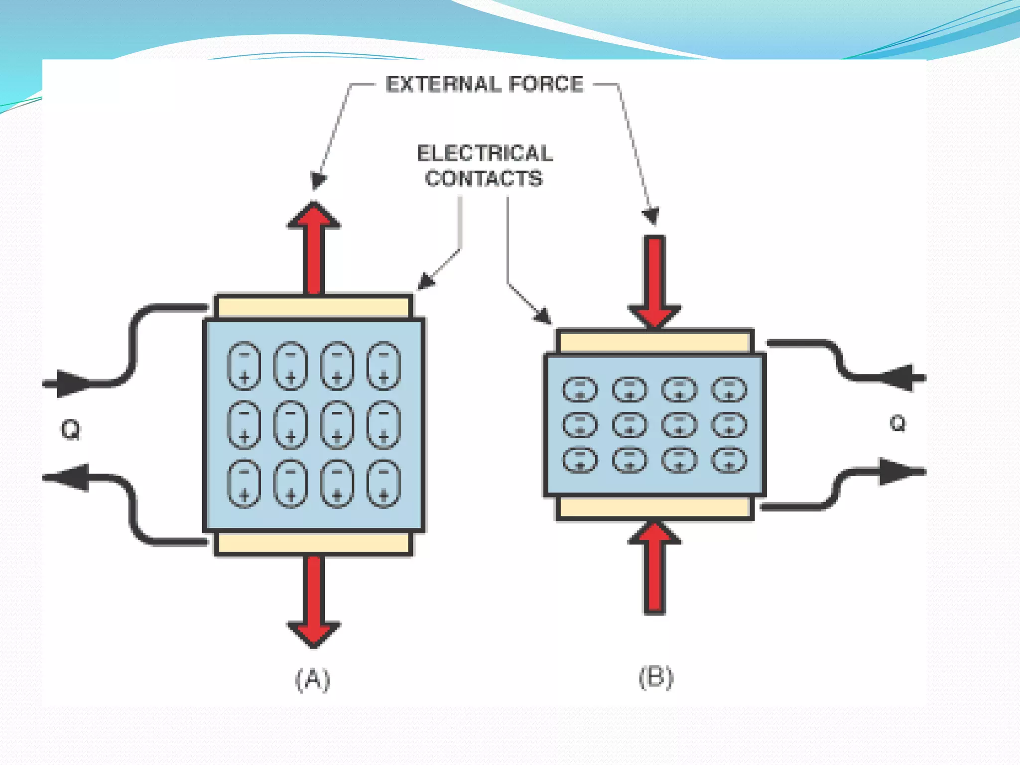
![The amount of charge produced is strictly
proportional to the applied force and independent of
the piezoelectric element size and shape. Putting
several elements mechanically in series and
electrically in parallel is the only way to increase the
charge output. The resulting charge is
{display style C_{x}=d_{xx}F_{x}n~},where {display
style d_{xx}} is the piezoelectric coefficient for a
charge in x-direction released by forces applied along
x-direction (in pC/N). {display style F_{x}} is the
applied Force in x-direction [N] and {display style
n} corresponds to the number of stacked elements.](https://image.slidesharecdn.com/piezoelectricsens0r-161226171056/75/Piezoelectric-sens0-r-11-2048.jpg)


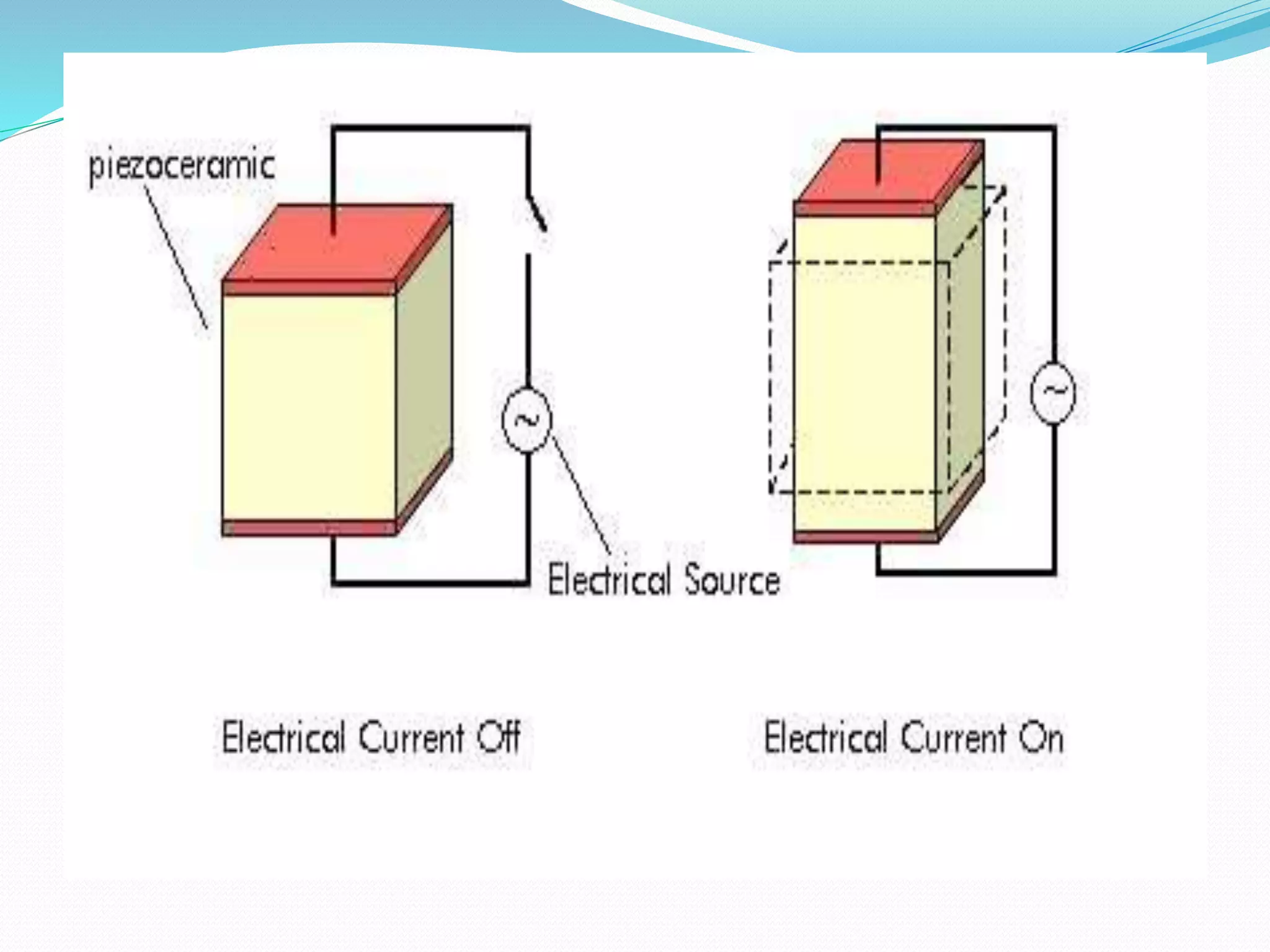


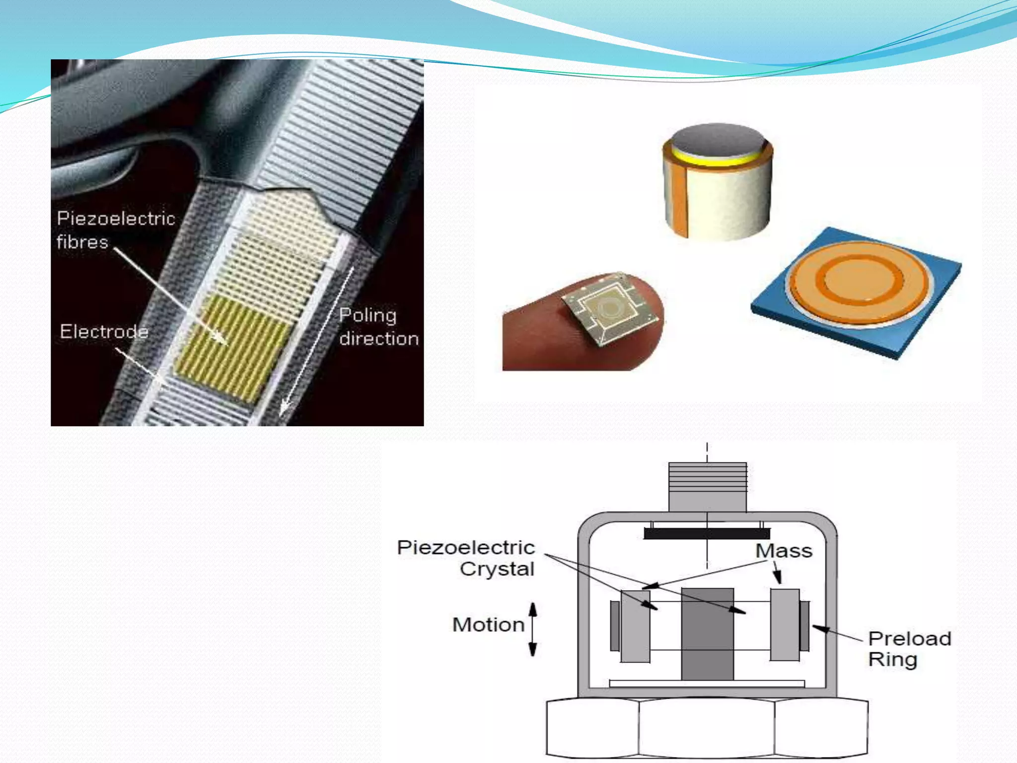
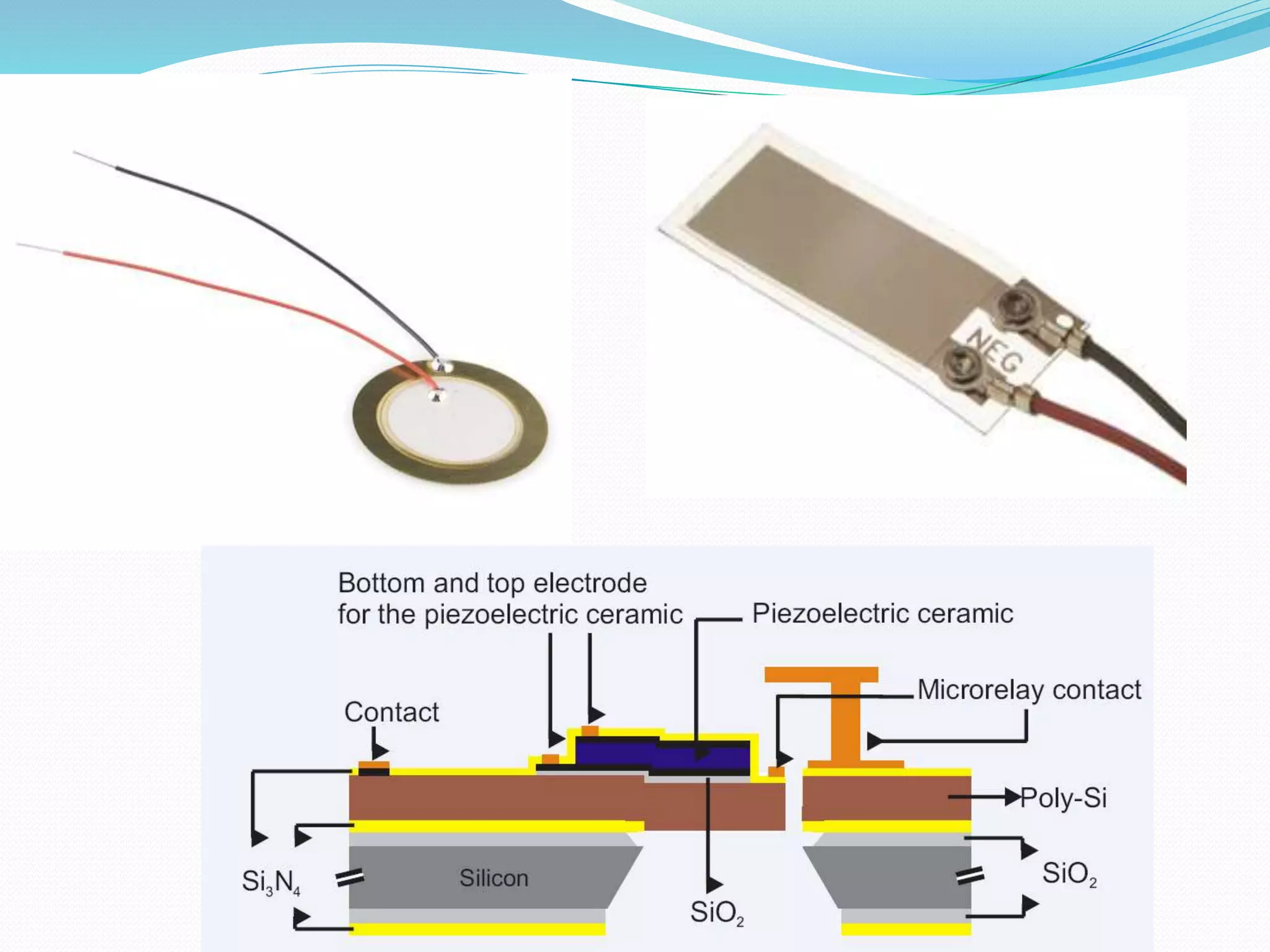
A piezoelectric sensor uses the piezoelectric effect to convert changes in pressure, acceleration, temperature, strain or force into an electrical charge. Piezoelectric sensors are versatile tools that are used for quality assurance, process control, and research and development across many industries. They have limitations for static measurements but are otherwise a mature and reliable sensing technology. Piezoresistive sensors undergo a change in electrical resistance when subjected to mechanical strain, and are commonly used in integrated circuits made from piezoresistive materials like silicon.


