Downloaded 186 times
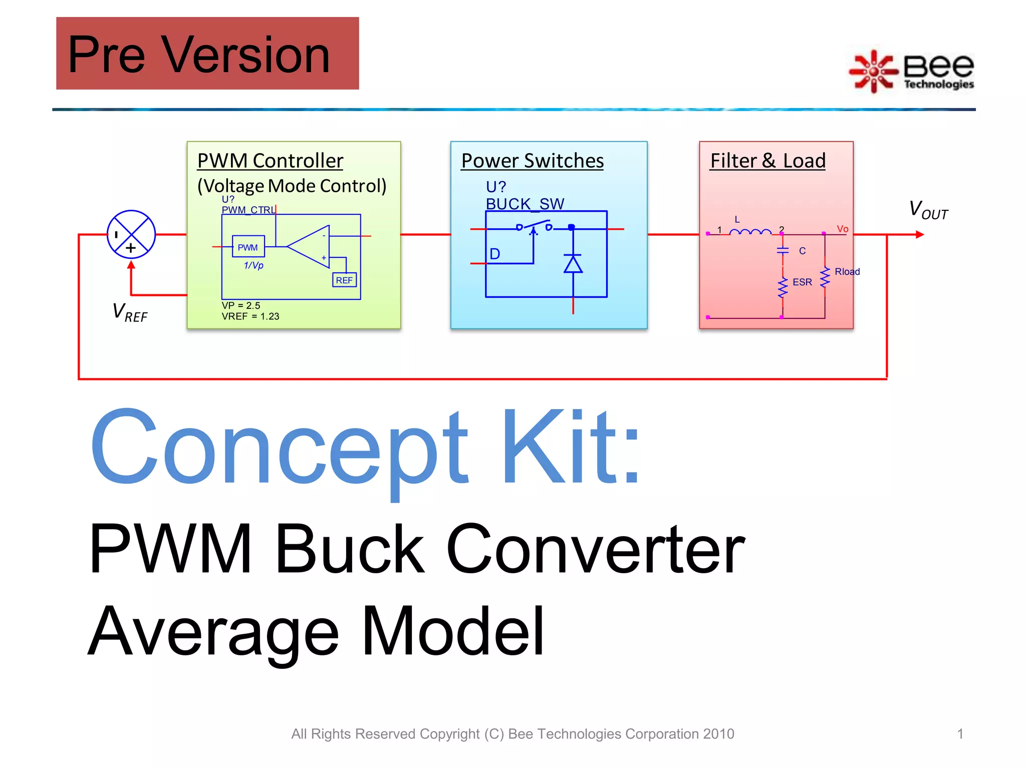
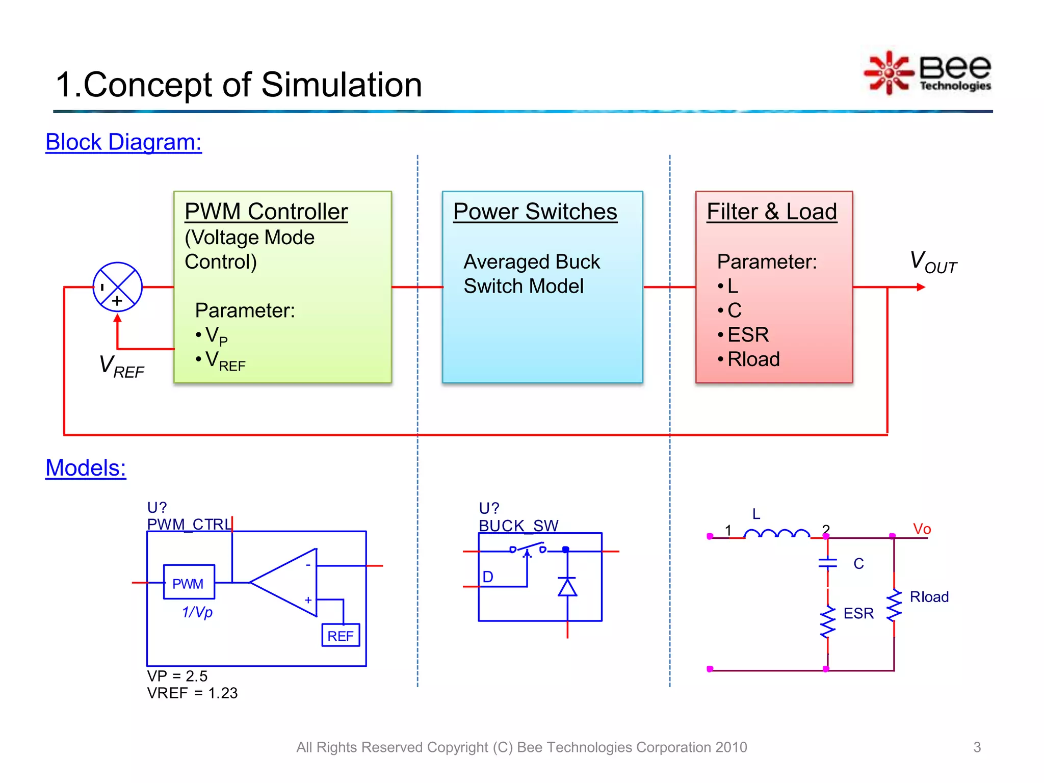
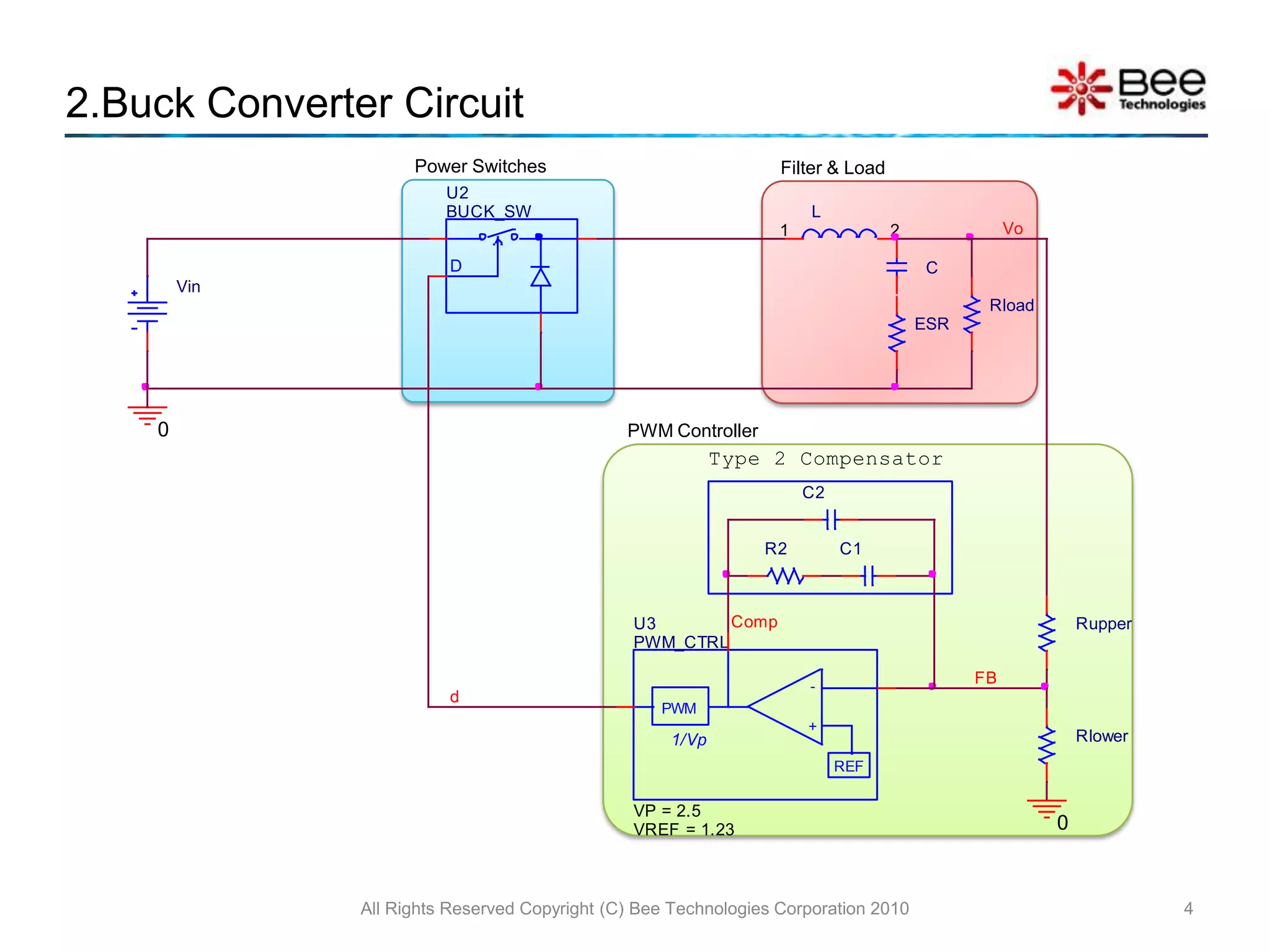
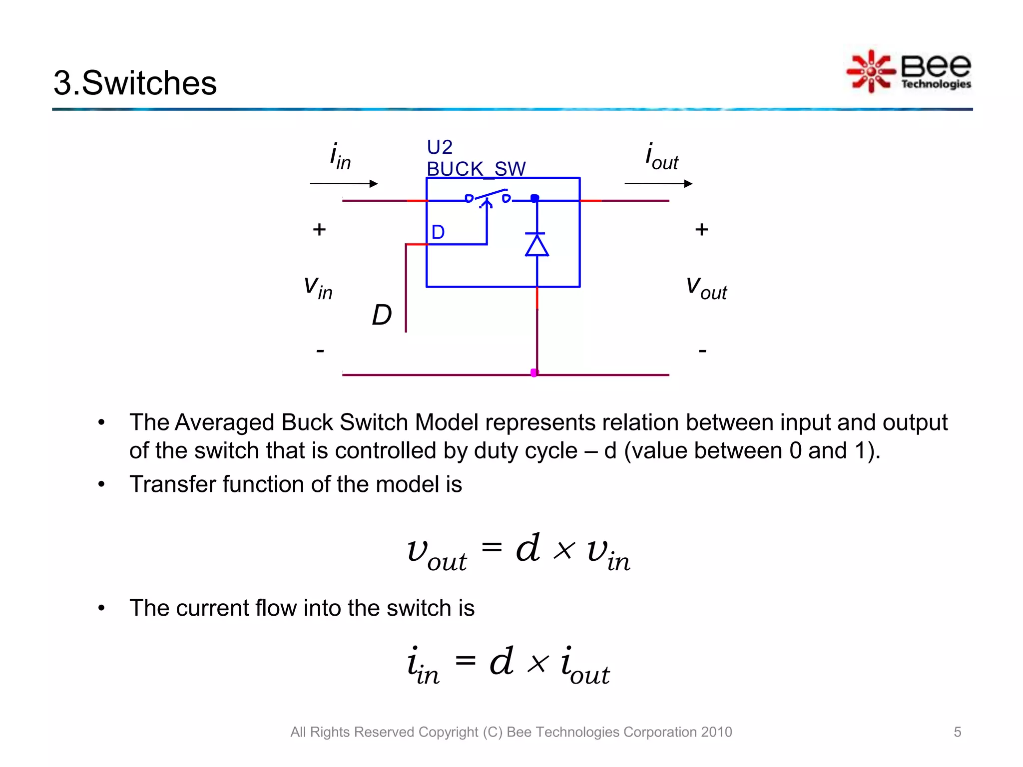
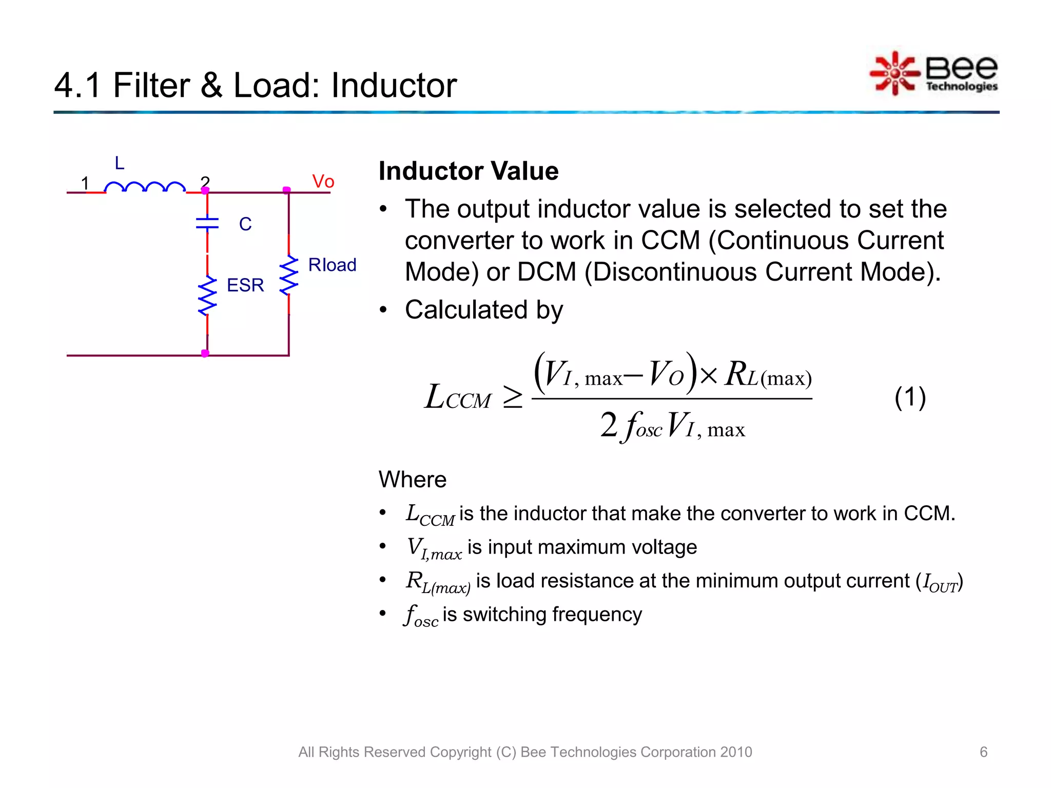
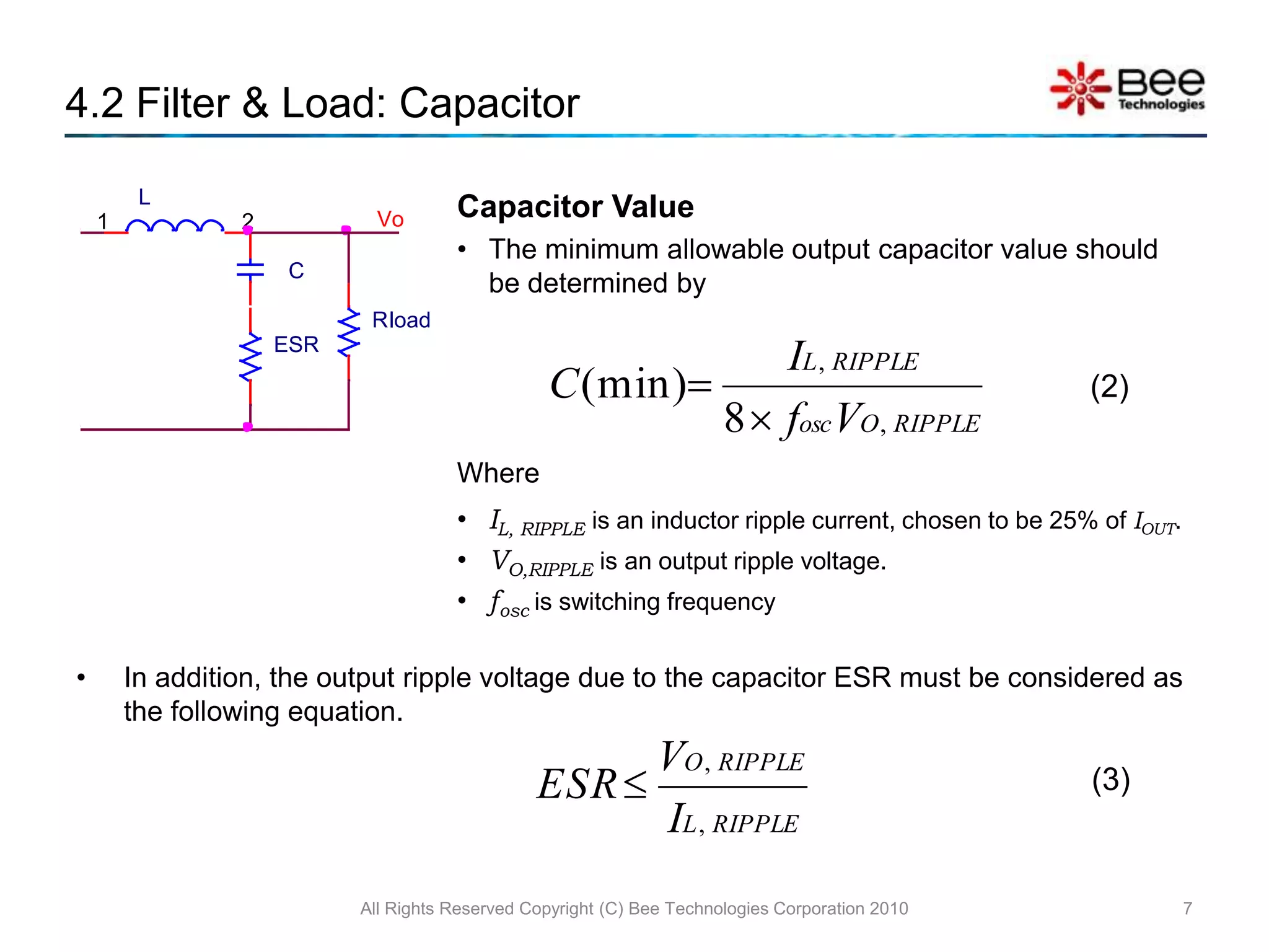
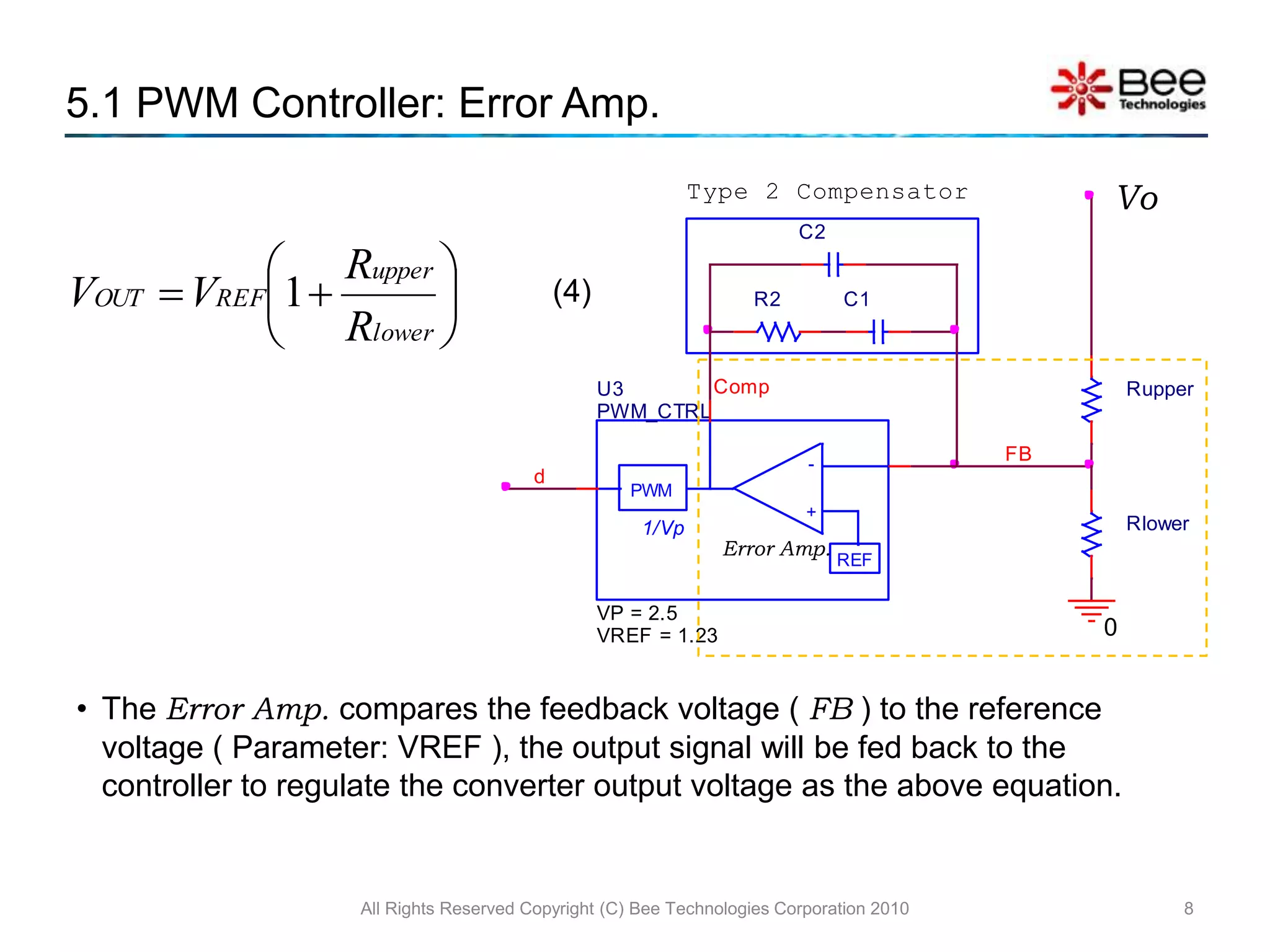
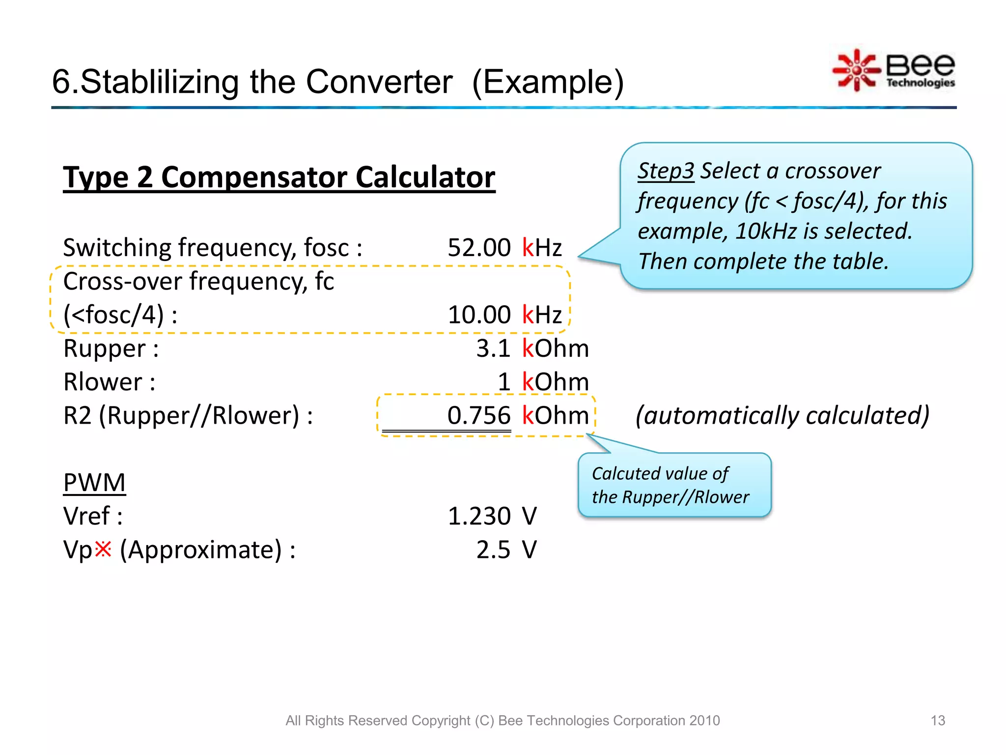
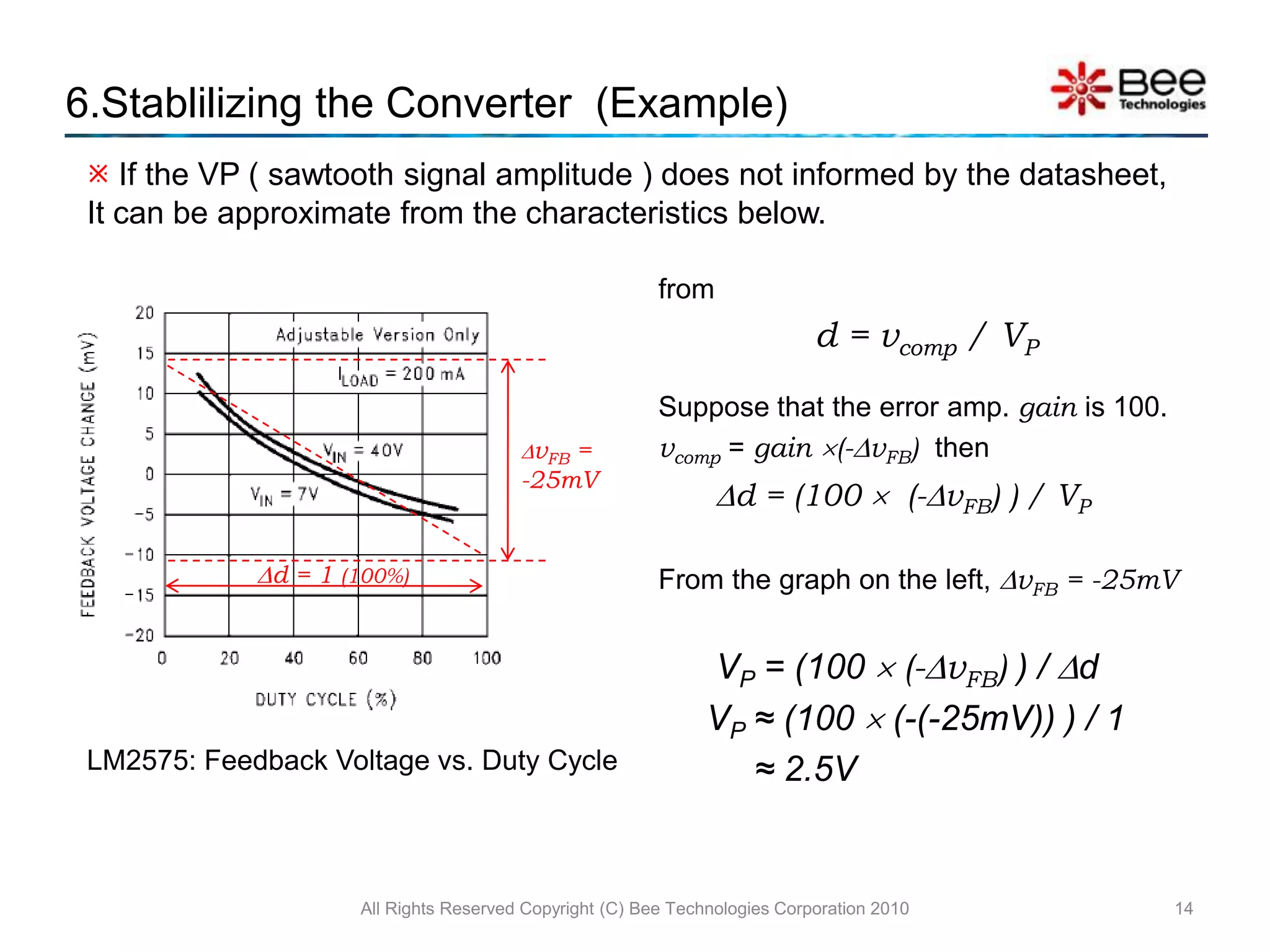
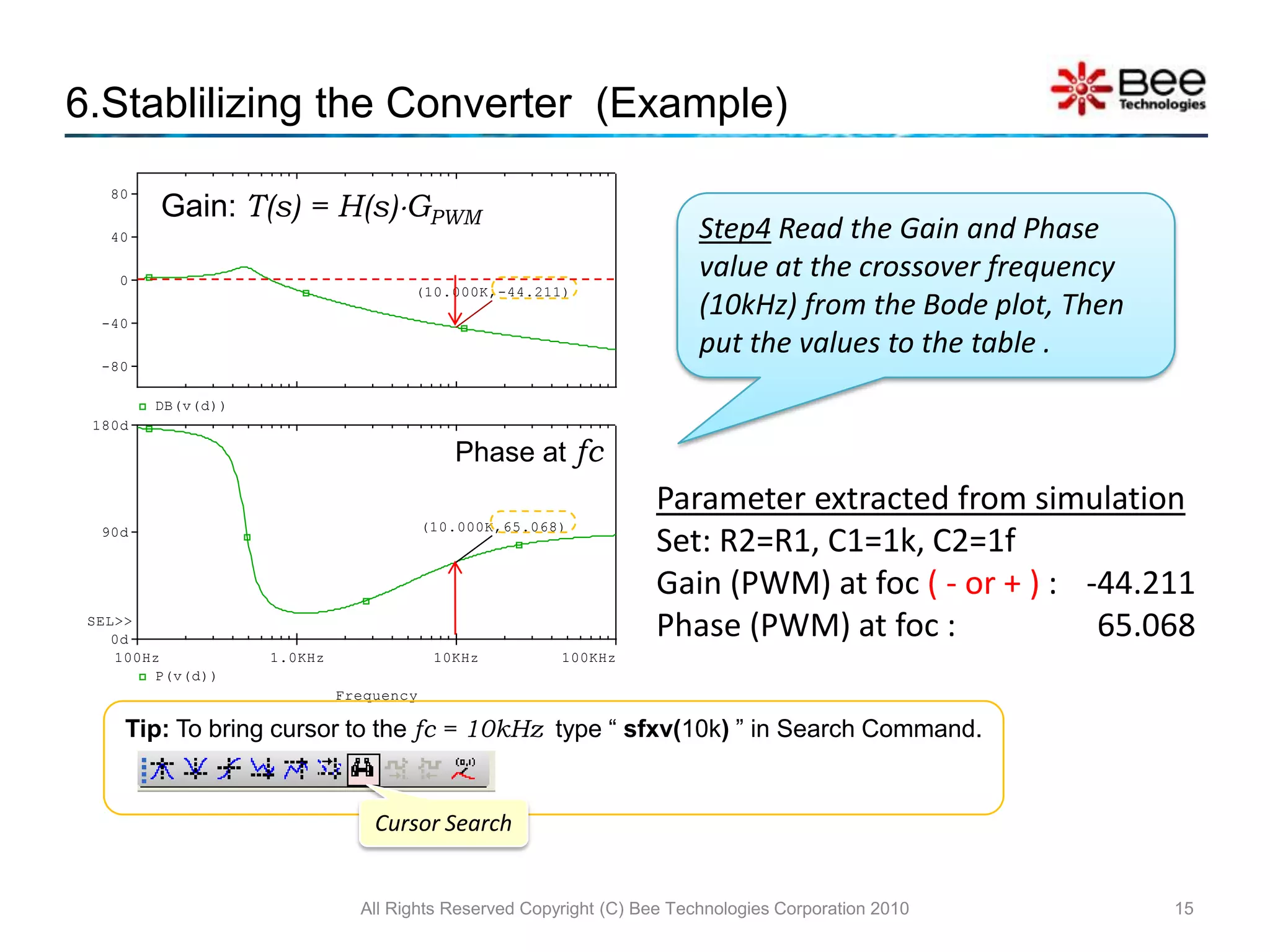
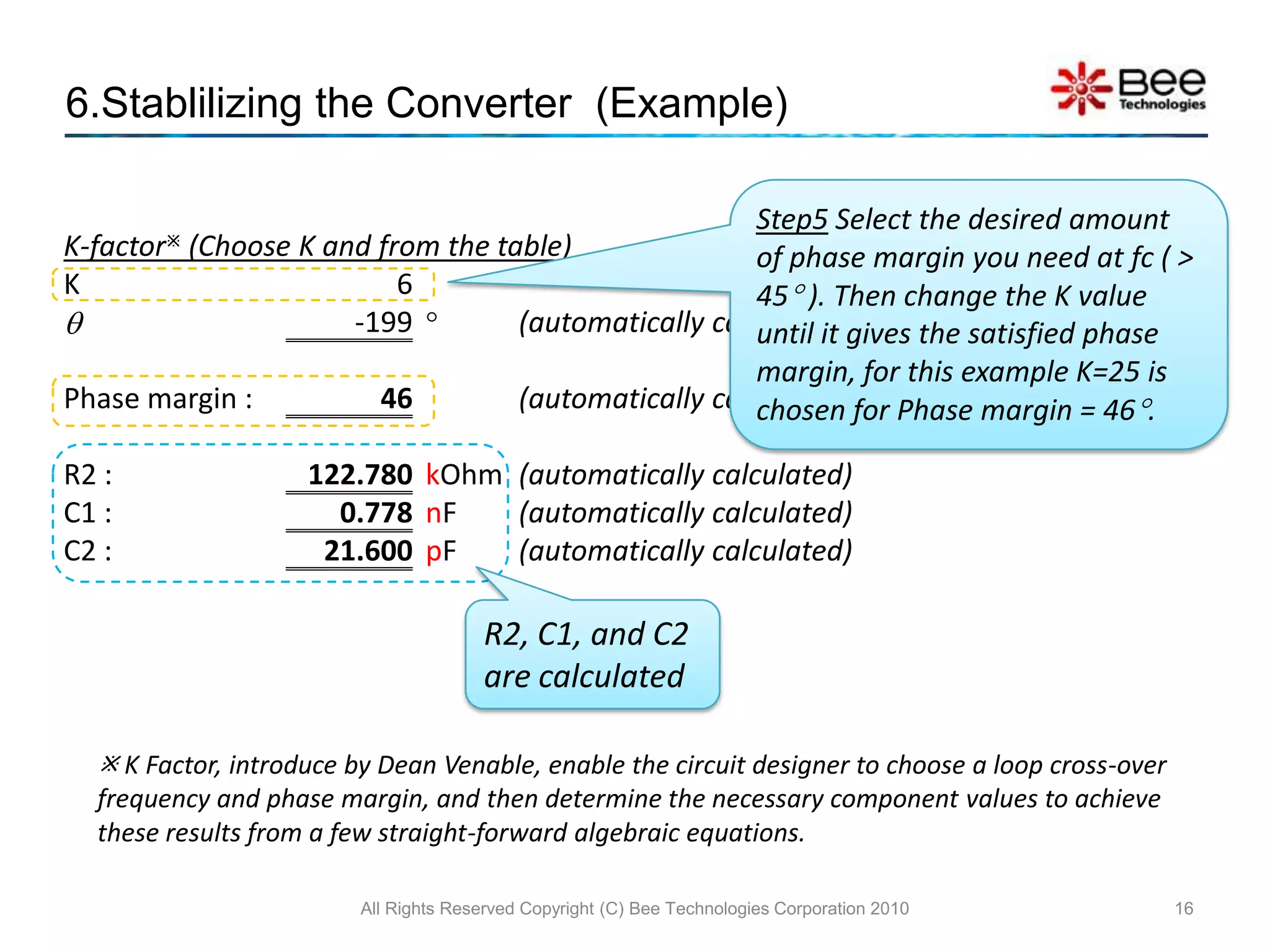
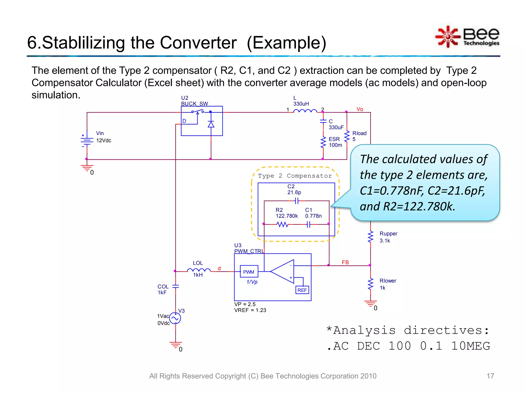
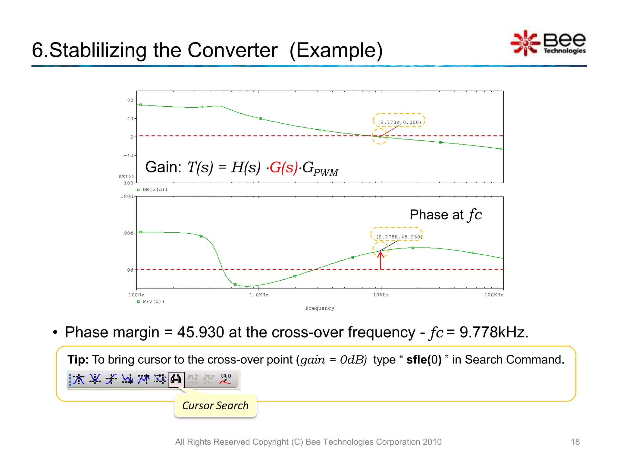
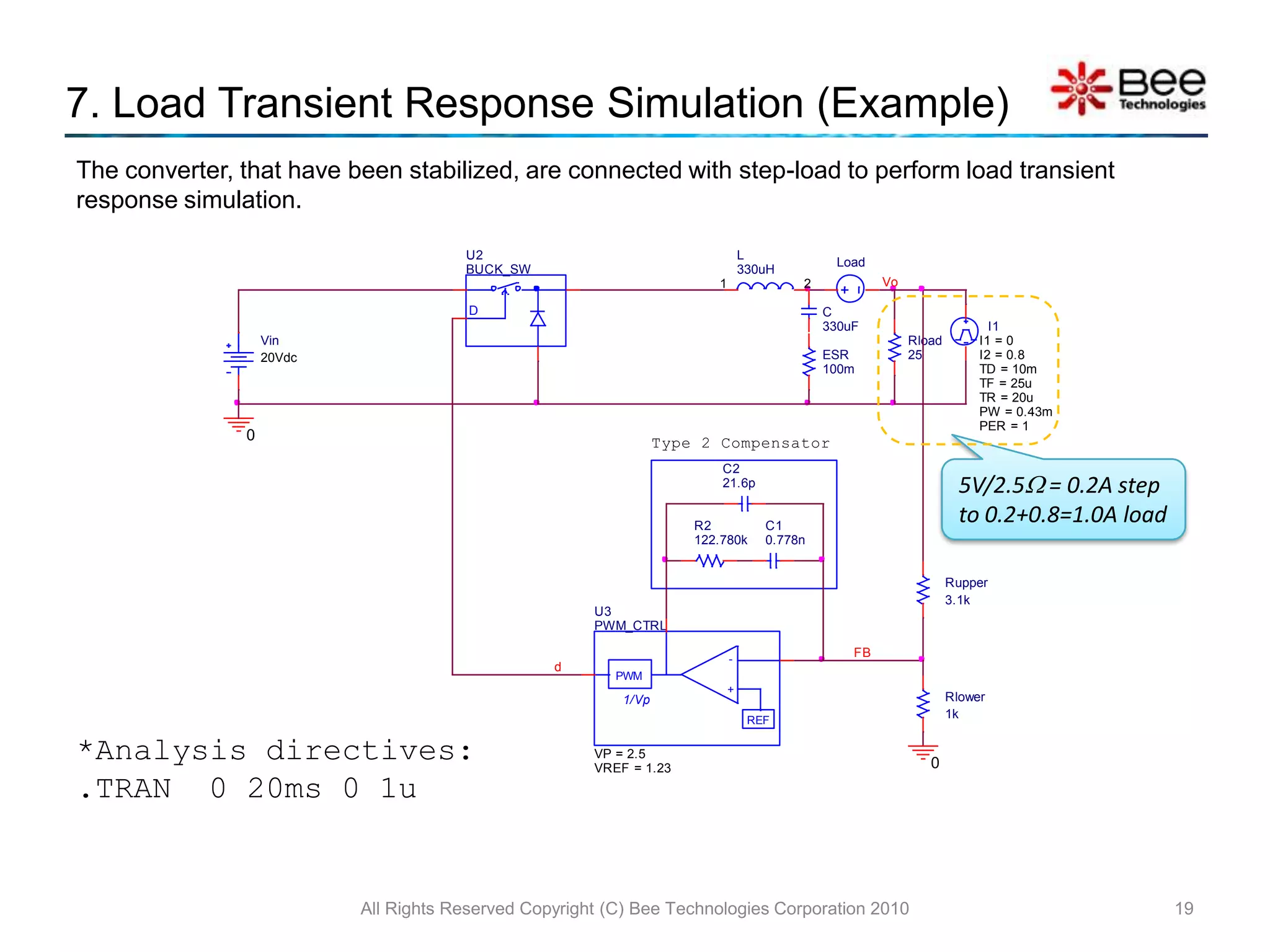
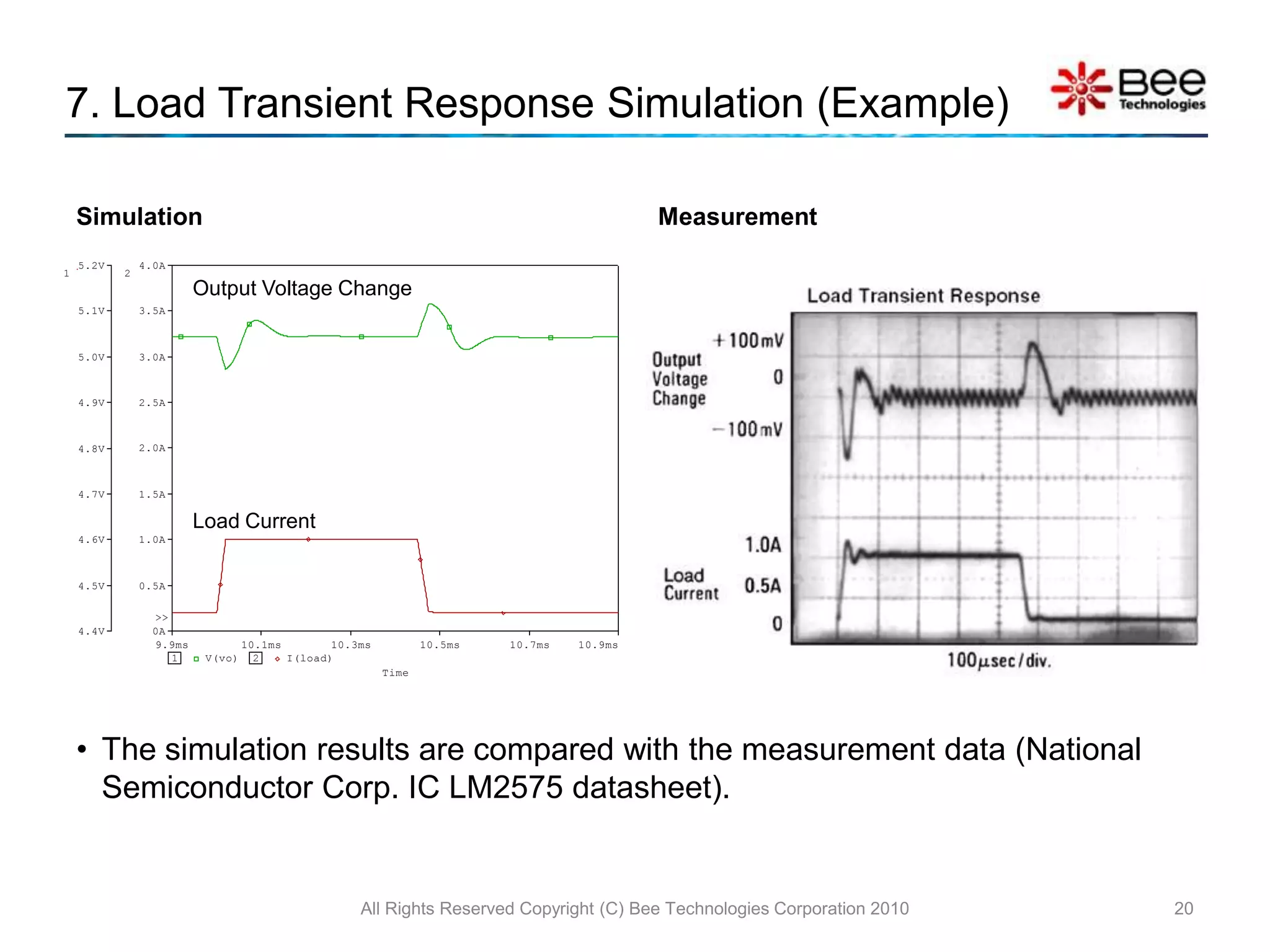
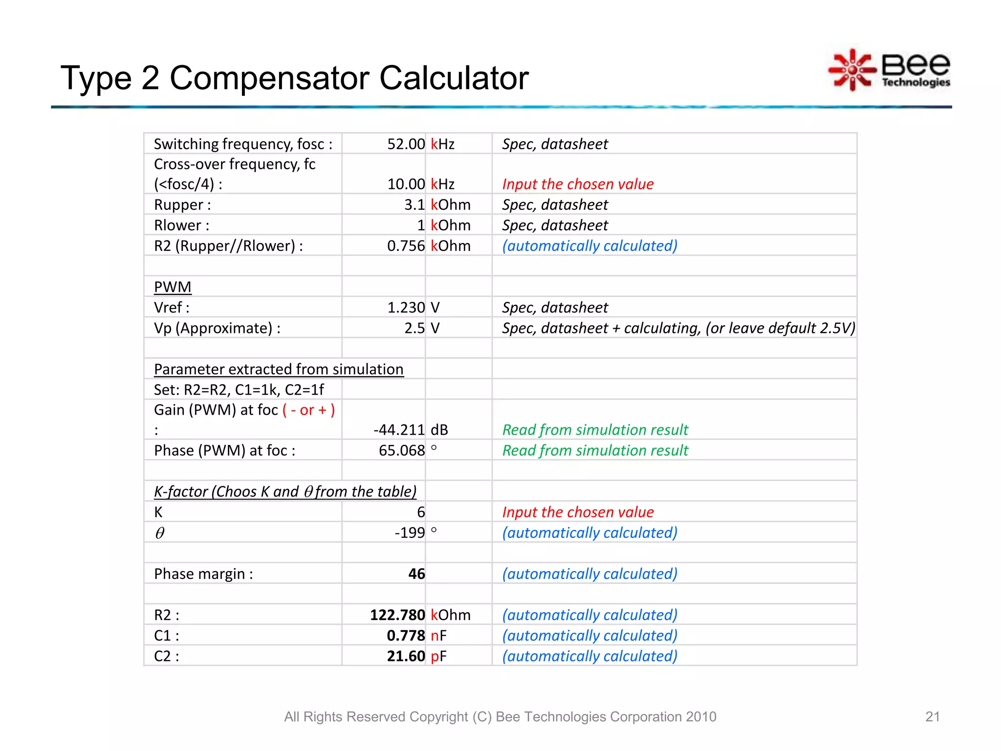
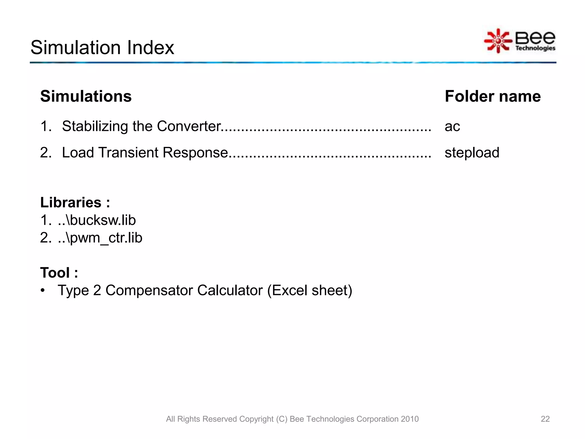

The document provides a detailed overview of a PWM buck converter average model, outlining its components, including switches, filters, loads, and PWM controllers. It discusses the methods to select inductor and capacitor values to ensure stable operation, as well as compensator design for stabilizing the converter. Examples of simulations and calculations related to load transient response and compensator values are included, demonstrating the practical application of the concepts presented.


