Download to read offline


![Omar A. Xacur (723009570) ECEN 607: Final Project Report
η =
Pout
Pin
=
Pin − PL
Pin
=
Po
Po + PL
(3)
Where PL is the power loss in the circuit and is define as:
PL = Pcd + Psw + Psc + PQ (4)
Pcd = Conduction losses due Ron.
Psw = Switching losses due charge and discharge of parasitics.
Psc = Short Circuit losses.
PQ = Quiescent power losses.
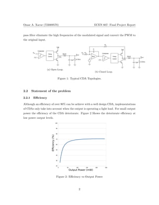
Previous works in Class D audio amplifiers only report the efficiency for a given load,
usually 8 ohms or 4 ohms. Nevertheless, in DC-DC converters the efficiency for different
output currents, and since DC-DC converters use a similar output stage as in the CDA, the
work done in that area is used as reference for the work in this project.
Figure 3: Results of [1]
[1] use a PMOS and NMOS output stage partitioned in three independently controlled
segments. The segments were created using identical unit cells connected in parallel to
achiever a binary weighting.
4](https://image.slidesharecdn.com/111e28a2-b29a-47e3-8217-e2aca71c2091-161102164854/85/FinalReport-4-320.jpg)
![Omar A. Xacur (723009570) ECEN 607: Final Project Report
3.2 PSR
Various works have been done regarding the enhancement of the PSR in the CDA. Some
works include high order compensator filters or bridge-tie loads, that usually bring trade-off
of power consumption or active area. A Feed-Forward technique is also implemented to
achieve high PSR in the CDA.
Figure 4: FFPSNC Technique Model [2]
The Feed-Forward module inject the noise into the system with the correct gain and
polarity to cancel the noise of the supply that can achieve a PSR of 83dB. [2]
5](https://image.slidesharecdn.com/111e28a2-b29a-47e3-8217-e2aca71c2091-161102164854/85/FinalReport-5-320.jpg)
![Omar A. Xacur (723009570) ECEN 607: Final Project Report
4 Proposed Solution
Based in the idea of [1], the proposed solution is to have an adaptive output stage for
different power output. A finite state machine will be choosing the optimal output stage
for a given output power.
Figure 5: Region of losses
Knowing the principal losses in any given region of power output, an optimal CDA
output stage can be designed.
Low Output Power Medium Output Power High Output Power
PL = Psw = V 2
DDCpfsw PL = Psw + Pcd = PL = Pcd = I2
outRon
V 2
DDCpfsw + I2
outRon
Table 1: Losses by region of power consumption
To not compromise the PSR in the design, the Feed-Forward technique mentioned in
previous section is implemented in this work to achieve high PSR performance.
6](https://image.slidesharecdn.com/111e28a2-b29a-47e3-8217-e2aca71c2091-161102164854/85/FinalReport-6-320.jpg)


![Omar A. Xacur (723009570) ECEN 607: Final Project Report
10 Discussion of Results with other reported results and sug-
gested improvements
The results for the output stage were favourables having an efficiency above 90% and an
enhancement little over 10%, but still this work can be considerate as a work in progress since
the PSR and THD are not competitive with another design in the market. Furthermore,
the reported results are measured with the fabricated device. This work is pretended to be
a starting point in the development of a competitive CDA.
10.1 Future Work
To improve the results of this projects, the FFPSNC needs to be revised carefully to improve
the PSR. Currently, due lack of time, the finite machine was not implemented, a research
into previous implementations of finite states needs to be done. Also, a inquire into the
enhancement of the THD needs to be done.
Parameter This work [2] [1]
Filter Order 1 1 NA
PSR(dB) 69 83 NA
η(%) 95 94 89
THD (%) 0.143 0.0149 NA
Supply(V) 3.3 1.8 4.2
Fsw(KHz) 500 500 4000
η Improvement 10 NA 7.5
Table 3: Comparison Table
References
[1] Oliver Trescases, et. al. A Digitally Controlled DC-DC Converter Module with a Seg-
mented Output Stage For Optimized Efficiency, International Symposium on Power
Semiconductors Devices & IC’s, June, 2006 Naples, Italy
15](https://image.slidesharecdn.com/111e28a2-b29a-47e3-8217-e2aca71c2091-161102164854/85/FinalReport-15-320.jpg)
![Omar A. Xacur (723009570) ECEN 607: Final Project Report
[2] A.I. Colli-Menchi; J. Torres; E. Snchez-Sinencio, A Feed-Forward Power-Supply Noise
Cancellation Technique for Single-Ended Class-D Audio Amplifiers, IEEE Journal of
Solid-State Circuits , vol.49, no.3, pp.718-728, March 2014
[3] Texas Instruments Inc., Dallas, TX, USA, TLV320AIC3107: Low-Power Stereo Au-
dio Codec With Integrated Mono Class-D Amplifier, Apr. 2009 [Online]. Available:
http://www.ti.com/lit/ds/slos619/ slos619.pdf
[4] M. A. Teplechuk et al., True filterless class-D audio amplifier, IEEE J. Solid-State
Circuits, vol. 46, no. 12, pp. 27842793, Dec. 2011
[5] Oliver TresCases, et al. Prefictive Efficiency Optimization for DC-DC Converters With
Highly Dynamic Digital Logic IEEE, Power Electronics, Vol. 23, No. 4 July 2008
[6] Wei Shu and Joseph S. Chang THD of Closed-Loop Analog PWM Class-D Amplifier
IEEE transactions on circuits and Systems-I: Regular Papers, Vol. 55, no.6, July 2008
[7] Adrian I Colli-Menchi, Miguel A Rojas-Gonzalez, Edgar Sanchez-Sinencio Design Tech-
niques for Integrated CMOS Class-D Audio Amplifiers, Advanced Series in Electrical
and Computer Engineering: Volume 16
16](https://image.slidesharecdn.com/111e28a2-b29a-47e3-8217-e2aca71c2091-161102164854/85/FinalReport-16-320.jpg)

This document summarizes an adaptive output stage Class D audio amplifier designed for high efficiency over a wide range of output powers. The design uses multiple output stages selected by a finite state machine to optimize efficiency based on the output power level. At low output powers, switching losses dominate, so a low-power stage is selected. At medium powers, both switching and conduction losses are significant, selecting a medium-power stage. At high powers, conduction losses dominate, selecting a high-power stage. A feed-forward technique is used to enhance power supply rejection. Simulation results show over 90% efficiency across output powers and a power supply rejection ratio of 69dB.


![Analysis and design_of_a_low-voltage_low-power[1]](https://cdn.slidesharecdn.com/ss_thumbnails/analysisanddesignofalow-voltagelow-power1-140802050345-phpapp02-thumbnail.jpg?width=640&height=640&fit=bounds)
