Module 05 Bio MEMS notes by Mysore University School of Engineering, Mysore, Prepared by Assistant Professor Thanmay J S, Department of Bio Medical and Robotic Engineering
Mysore University Schoolof Engineering
8J99+QC7, Manasa Gangothiri, Mysuru, Karnataka 570006
Prepared by: Mr Thanmay J S, Assistant Professor, Bio-Medical & Robotics Engineering, UoM, SoE, Mysore 57006
Module 05: Course Content
5.0 Introduction to Microsystem Fabrication Process
5.1 Photolithography
5.2 Ion Implantation
5.3 Diffusion
5.4 Oxidation
5.5 Chemical Vapour Deposition
5.6 Physical Vapour Deposition
5.7 Deposition by Epitaxy
5.8 Etching
5.9 The LIGA Process
3.
Mysore University Schoolof Engineering
8J99+QC7, Manasa Gangothiri, Mysuru, Karnataka 570006
Prepared by: Mr Thanmay J S, Assistant Professor, Bio-Medical & Robotics Engineering, UoM, SoE, Mysore 57006
5.0 Introduction to Microsystem Fabrication Process
Microsystem fabrication refers to the processes and techniques used to create miniature devices and systems
with critical components at the micrometer (µm) scale. These devices are commonly found in
microelectromechanical systems (MEMS), which are integrated systems that combine mechanical elements,
sensors, actuators, and electronics. The process involves various steps of material deposition, patterning,
etching, doping, and more, to create the desired structure. Fabrication typically follows a series of steps:
• Substrate preparation: Clean and treat the substrate material.
• Thin-film deposition: Apply thin layers of materials such as silicon, metal, or dielectric.
• Patterning: Define features using photolithography or other methods.
• Etching: Remove unwanted material from the surface.
• Material modification: Alter properties (e.g., doping or diffusion).
• Packaging and integration: Assemble the microsystem into a functional unit.
These Microsystem fabrication processes are foundational to the field of microsystem fabrication and MEMS
technology, enabling the creation of devices that have applications across industries, including
telecommunications, automotive, healthcare, and consumer electronics.
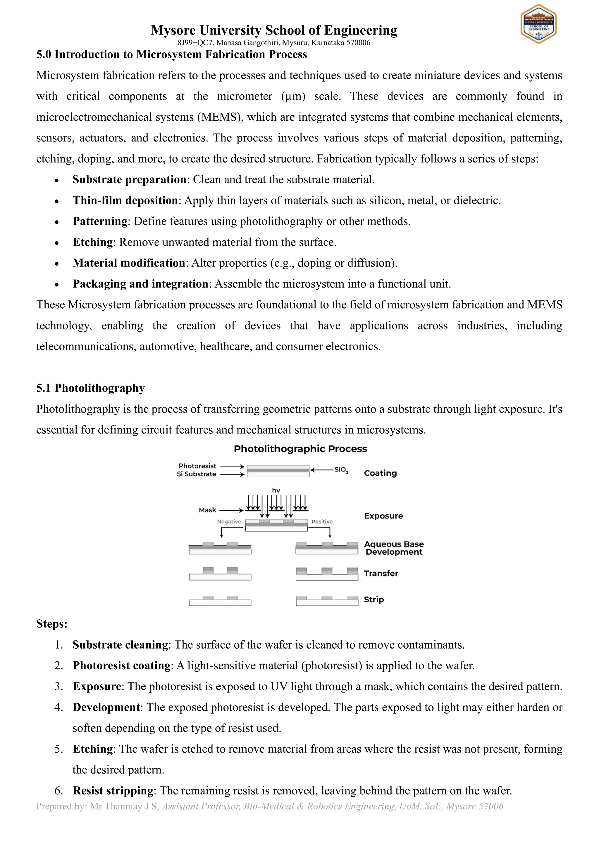
5.1 Photolithography
Photolithography is the process of transferring geometric patterns onto a substrate through light exposure. It's
essential for defining circuit features and mechanical structures in microsystems.
Steps:
1. Substrate cleaning: The surface of the wafer is cleaned to remove contaminants.
2. Photoresist coating: A light-sensitive material (photoresist) is applied to the wafer.
3. Exposure: The photoresist is exposed to UV light through a mask, which contains the desired pattern.
4. Development: The exposed photoresist is developed. The parts exposed to light may either harden or
soften depending on the type of resist used.
5. Etching: The wafer is etched to remove material from areas where the resist was not present, forming
the desired pattern.
6. Resist stripping: The remaining resist is removed, leaving behind the pattern on the wafer.
4.
Mysore University Schoolof Engineering
8J99+QC7, Manasa Gangothiri, Mysuru, Karnataka 570006
Prepared by: Mr Thanmay J S, Assistant Professor, Bio-Medical & Robotics Engineering, UoM, SoE, Mysore 57006
5.2 Ion Implantation
Ion implantation is a process used to alter the electrical properties of a semiconductor by introducing dopants
into the material.
Steps:
1. Ion source preparation: A dopant gas is ionized into charged particles (ions).
2. Acceleration: The ions are accelerated toward the substrate using an electric field.
3. Implantation: The accelerated ions collide with the substrate and penetrate its surface, embedding
themselves into the material.
4. Annealing: The wafer is heated to activate the dopants and repair damage to the crystal structure.
5.3 Diffusion
Diffusion is the process of driving dopants into a substrate material (typically silicon) using heat.
Steps:
1. Wafer cleaning: The wafer is cleaned to remove any contamination.
2. Dopant source: A solid or gaseous dopant source is used, often placed in a diffusion furnace.
3. Heating: The wafer is heated to a specific temperature (typically 900-1100°C) to encourage dopants
to diffuse into the silicon.
4. Dopant diffusion: Over time, the dopants spread throughout the silicon wafer.
5. Cooling: The wafer is slowly cooled to prevent thermal shock and to finalize the diffusion process.
5.
Mysore University Schoolof Engineering
8J99+QC7, Manasa Gangothiri, Mysuru, Karnataka 570006
Prepared by: Mr Thanmay J S, Assistant Professor, Bio-Medical & Robotics Engineering, UoM, SoE, Mysore 57006
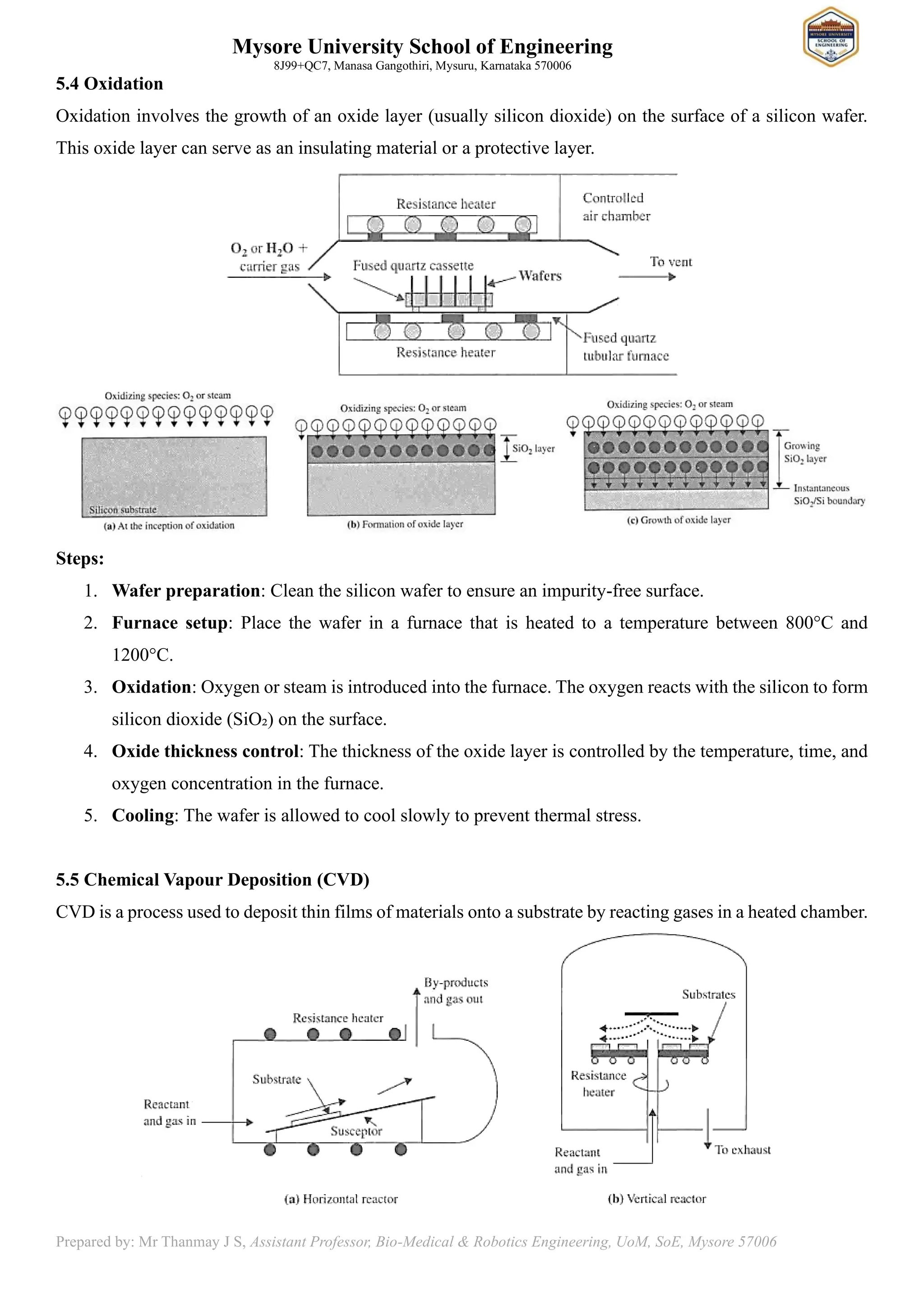
5.4 Oxidation
Oxidation involves the growth of an oxide layer (usually silicon dioxide) on the surface of a silicon wafer.
This oxide layer can serve as an insulating material or a protective layer.
Steps:
1. Wafer preparation: Clean the silicon wafer to ensure an impurity-free surface.
2. Furnace setup: Place the wafer in a furnace that is heated to a temperature between 800°C and
1200°C.
3. Oxidation: Oxygen or steam is introduced into the furnace. The oxygen reacts with the silicon to form
silicon dioxide (SiO₂) on the surface.
4. Oxide thickness control: The thickness of the oxide layer is controlled by the temperature, time, and
oxygen concentration in the furnace.
5. Cooling: The wafer is allowed to cool slowly to prevent thermal stress.
5.5 Chemical Vapour Deposition (CVD)
CVD is a process used to deposit thin films of materials onto a substrate by reacting gases in a heated chamber.
6.
Mysore University Schoolof Engineering
8J99+QC7, Manasa Gangothiri, Mysuru, Karnataka 570006
Prepared by: Mr Thanmay J S, Assistant Professor, Bio-Medical & Robotics Engineering, UoM, SoE, Mysore 57006
Steps:
1. Gas introduction: Gaseous precursors are introduced into a reaction chamber.
2. Decomposition: The gases decompose chemically due to the heat or plasma inside the chamber.
3. Film deposition: The reaction products deposit onto the surface of the substrate, forming a thin film.
4. Wafer removal: The substrate is removed from the chamber after the deposition process.
CVD can be further classified into various types, including low-pressure CVD (LPCVD) and plasma-
enhanced CVD (PECVD), depending on the process conditions.
5.6 Physical Vapour Deposition (PVD)
PVD is a vacuum deposition process used to deposit thin films by
physical processes such as evaporation or sputtering.
Steps:
1. Source material: A material (metal or other) is heated to a
vapor state in a vacuum chamber.
2. Vaporization: The material evaporates or is bombarded by
ions, converting it into vapor.
3. Deposition: The vapor condenses and adheres to the
substrate, forming a thin film.
4. Cooling: After deposition, the substrate is cooled, and the thin film solidifies.
Common methods of PVD include thermal evaporation and sputtering.
5.7 Deposition by Epitaxy
Epitaxy is the process of growing a thin layer of crystalline material on a substrate in which the deposited
material's crystal structure follows that of the substrate.
Steps:
1. Substrate preparation: The substrate
surface is cleaned and prepared.
2. Growth initiation: Epitaxial growth begins
in a vacuum or gas environment, typically
under controlled conditions of temperature
and pressure.
3. Material deposition: Material is deposited in a way that allows the new layer to follow the crystalline
structure of the underlying substrate.
4. Control of growth: Parameters such as temperature, pressure, and gas composition are carefully
controlled to ensure proper crystal formation.
Epitaxial layers are often used to create high-quality semiconductor layers for devices like transistors.
7.
Mysore University Schoolof Engineering
8J99+QC7, Manasa Gangothiri, Mysuru, Karnataka 570006
Prepared by: Mr Thanmay J S, Assistant Professor, Bio-Medical & Robotics Engineering, UoM, SoE, Mysore 57006
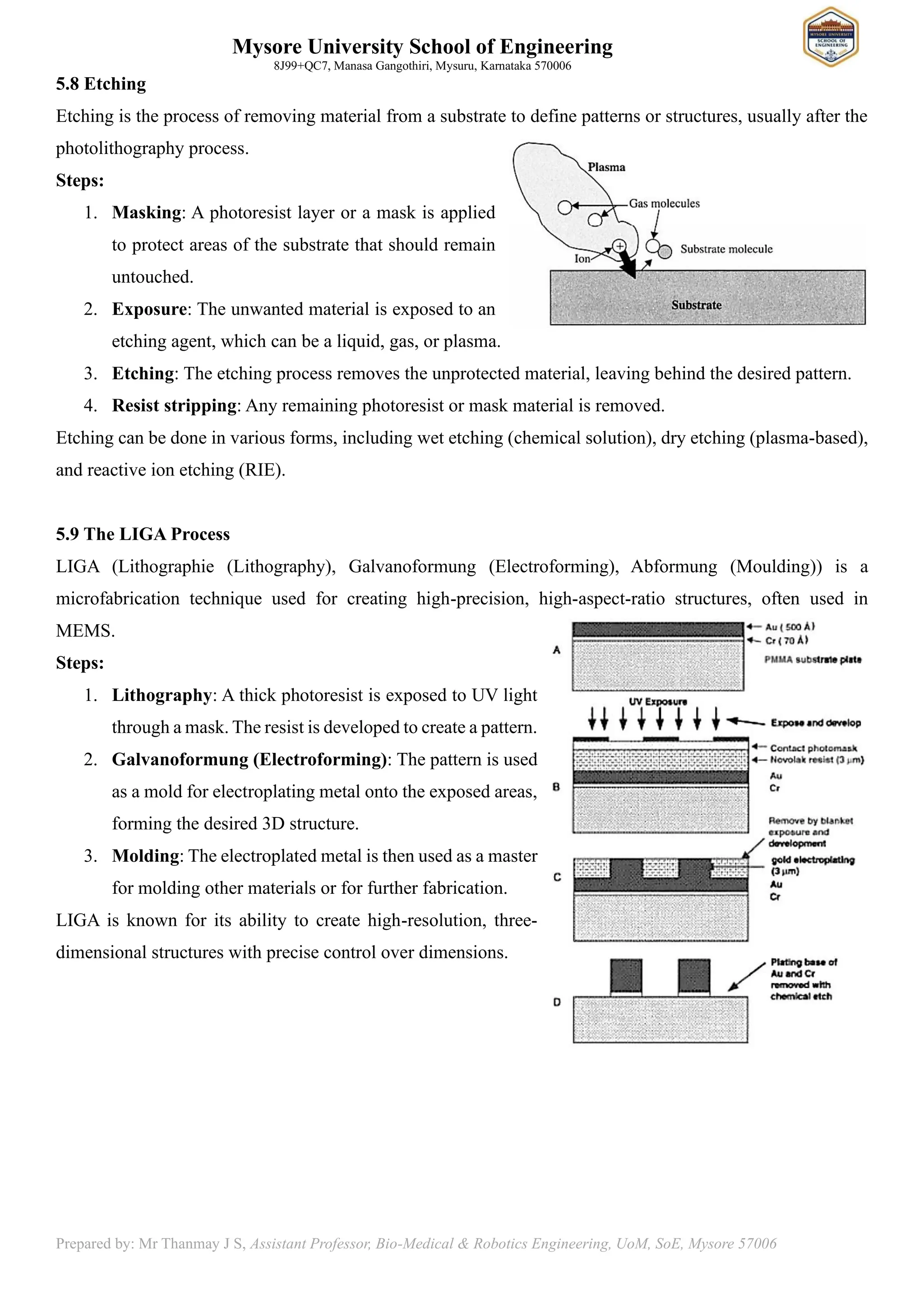
5.8 Etching
Etching is the process of removing material from a substrate to define patterns or structures, usually after the
photolithography process.
Steps:
1. Masking: A photoresist layer or a mask is applied
to protect areas of the substrate that should remain
untouched.
2. Exposure: The unwanted material is exposed to an
etching agent, which can be a liquid, gas, or plasma.
3. Etching: The etching process removes the unprotected material, leaving behind the desired pattern.
4. Resist stripping: Any remaining photoresist or mask material is removed.
Etching can be done in various forms, including wet etching (chemical solution), dry etching (plasma-based),
and reactive ion etching (RIE).
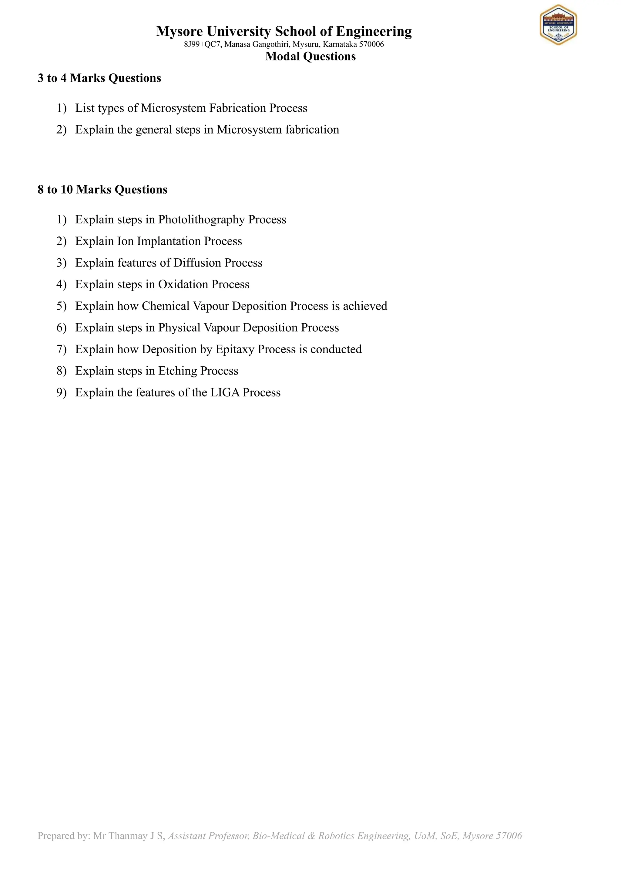
5.9 The LIGA Process
LIGA (Lithographie (Lithography), Galvanoformung (Electroforming), Abformung (Moulding)) is a
microfabrication technique used for creating high-precision, high-aspect-ratio structures, often used in
MEMS.
Steps:
1. Lithography: A thick photoresist is exposed to UV light
through a mask. The resist is developed to create a pattern.
2. Galvanoformung (Electroforming): The pattern is used
as a mold for electroplating metal onto the exposed areas,
forming the desired 3D structure.
3. Molding: The electroplated metal is then used as a master
for molding other materials or for further fabrication.
LIGA is known for its ability to create high-resolution, three-
dimensional structures with precise control over dimensions.
8.
Mysore University Schoolof Engineering
8J99+QC7, Manasa Gangothiri, Mysuru, Karnataka 570006
Prepared by: Mr Thanmay J S, Assistant Professor, Bio-Medical & Robotics Engineering, UoM, SoE, Mysore 57006
Modal Questions
3 to 4 Marks Questions
1) List types of Microsystem Fabrication Process
2) Explain the general steps in Microsystem fabrication
8 to 10 Marks Questions
1) Explain steps in Photolithography Process
2) Explain Ion Implantation Process
3) Explain features of Diffusion Process
4) Explain steps in Oxidation Process
5) Explain how Chemical Vapour Deposition Process is achieved
6) Explain steps in Physical Vapour Deposition Process
7) Explain how Deposition by Epitaxy Process is conducted
8) Explain steps in Etching Process
9) Explain the features of the LIGA Process