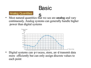
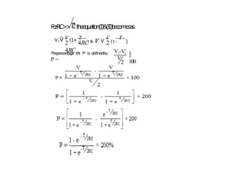
Basic
s
Analog Quantities
1 23 4 5 6 7 8 9 10 11 12 1 2 3 4 5 6 7 8 9 10 11 12
• Digital systems can A
p.M
r.
ocess, store, anP.M
d.
transmit data
more efficiently but can only assign discrete values to
each point
• Most natural quantities that we see are analog and vary
continuously. Analog systems can generally handle higher
power than digital systems
Temperature
(F)
100
95
90
85
80
75
70
Time of day
4.
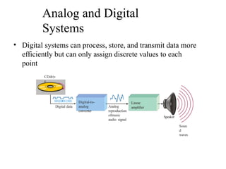
Analog and Digital
Systems
•Digital systems can process, store, and transmit data more
efficiently but can only assign discrete values to each
point
CDdriv
e
10110011101
Digital data Analog
reproduction
ofmusic
audio signal
Speaker
Soun
d
waves
Digital-to-
analog
converter
Linear
amplifier
5.
Contd.
.
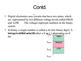
• Digital electronicsuses circuits that have two states, which
are represented by two different voltage levels called HIGH
and LOW. The voltages represent numbers in the binary
system
• In binary, a single number is called a bit (for binary digit). A
bit can have the value of either a 0 or a 1, depending on if
the
voltage is HIGH or LOW. VH(ma
x
VH(min
VL(max
VL(min
HIGH
INVALID
LOW
6.
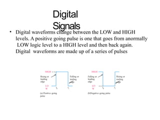
Digital
Signals
• Digital waveformschange between the LOW and HIGH
levels. A positive going pulse is one that goes from anormally
LOW logic level to a HIGH level and then back again.
Digital waveforms are made up of a series of pulses
(b)Negative–going pulse
HIGH
Falling or
leading
edge
Rising or
trailing
edge
LO
W
(a) Positive–going
pulse
HIGH
Rising or
leading
edge
Falling or
trailing
edge
LO
W
t0
t1
t0
t1
7.
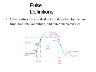
Pulse
Definitions
• Actual pulsesare not ideal but are described by the rise
time, fall time, amplitude, and other characteristics.
50%
10%
Baseline
Pulse
width
Risetime Fall
time
Amplitude tW
tr tf
Undershoot
Ringing
Overshoot
Ringing
Droop
90%
8.
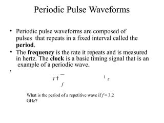
Periodic Pulse Waveforms
•Periodic pulse waveforms are composed of
pulses that repeats in a fixed interval called the
period.
• The frequency is the rate it repeats and is measured
in hertz. The clock is a basic timing signal that is an
example of a periodic wave.
•
T 1 z
f
What is the period of a repetitive wave if f = 3.2
GHz?
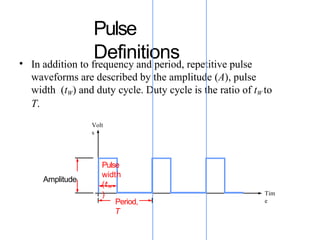
9.
Pulse
Definitions
• In additionto frequency and period, repetitive pulse
waveforms are described by the amplitude (A), pulse
width (tW) and duty cycle. Duty cycle is the ratio of tW to
T.
Volt
s
Pulse
width
(tW
) Tim
e
Period,
T
Amplitude
10.
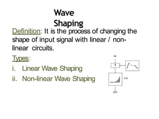
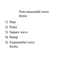
Wave
Shaping
Definition: It isthe process of changing the
shape of input signal with linear / non-
linear circuits.
Types:
i. Linear Wave Shaping
ii. Non-linear Wave Shaping
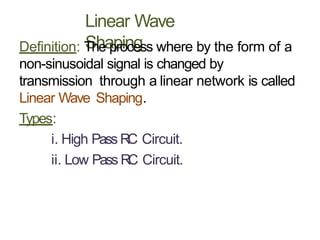
11.
Linear Wave
Shaping
Definition: Theprocess where by the form of a
non-sinusoidal signal is changed by
transmission through a linear network is called
Linear Wave Shaping.
Types:
i. High Pass RC Circuit.
ii. Low Pass RC Circuit.
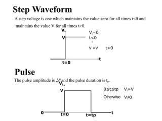
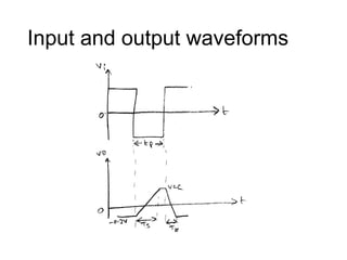
Step Waveform
t
t=0
i
Vi=0
t<0
V =Vt>0
A step voltage is one which maintains the value zero for all times t<0 and
maintains the value V for all times t>0.
Vi
V
Pulse
The pulse amplitude is „
V
‟and the pulse duration is tp.
0≤t≤tp
Otherwise
Vi=V
Vi=0
t=tp
t
Vi
V
t=0
0
14.
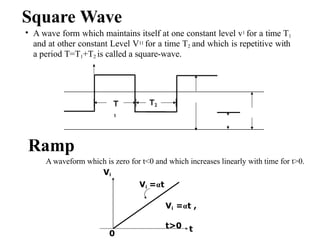
Square Wave
• Awave form which maintains itself at one constant level v1 for a time T1
and at other constant Level V11 for a time T2 and which is repetitive with
a period T=T1+T2 is called a square-wave.
T
1
T2
Ramp
A waveform which is zero for t<0 and which increases linearly with time for t>0.
Vi
Vi =αt
Vi =αt ,
t>0
0
t
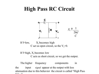
High Pass RCCircuit
R
+
Vo
C
+
-
Vi
-
If f=low, Xc becomes high
C act as open circuit, so the Vo=0.
If f=high, Xc becomes low
C acts as short circuit, so we get the output.
The higher frequency components in
the input signal appear at the output with less
attenuation due to this behavior the circuit is called “High Pass
XC 1
2f
C
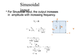
17.
Sinusoidal
input
+
V
O
i
+
Vin
_
_
• For Sinusoidalinput, the output increases
in amplitude with increasing frequency.
C
R
V V
i = =
in
R - j X C R -
in
j
2πf C
Vi
n
i=
R
1-
j
2πfRC
O
Vin ×R
Vi
n
V =i R= =
1- j
2πfR
C
j
R
1-
2πfR
C
Vo= iR
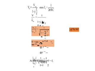
18.
V
O
1
=
Vin
1+j -
f1
f
1
=
VO
Vin 1 +
2
f1
f
θ =-tan -
1
-f1 =
tan-
1
f1
f
f
At the frequency f = f1
Vi
n
VO =
1 = 1
=0.707
1+1 2
A 0.707
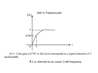
19.
At f =f1 the gain is 0.707 or this level corresponds to a signal reduction of 3
decibels(dB).
f1 is referred to as Lower 3-dB frequency.
20.
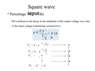
Square wave
input
• PercentageTilt ( 0
0 Tilt)
Tilt is defined as the decay in the amplitude of the output voltage wave due
to the input voltage maintaining constant level
2
1
X 10
0
P 1
V
V V 1
- T 1
R C
V '
1 = V 1. e
- T 2
R
C
V'
2 = V2 . e
2
V '
1 - V
=
V
V - V ' = V
1 2
(1
)
(2
)
(3
)
(4
)
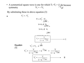
21.
& because
of
• Asymmetrical square wave is one for which T1=T2 =
symmetry V1 = - V2
By substituting these in above equation (3)
•
-T2RC -
V=V1.e V2
-T2RC+
V=V1.e V1
-T2RC
V
=
V1(1+e )
I
Equation
(1)
II
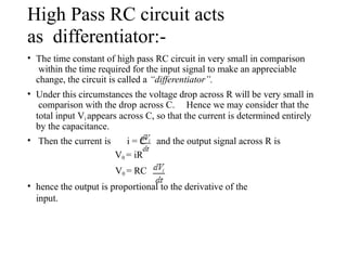
High Pass RCcircuit acts
as differentiator:-
• The time constant of high pass RC circuit in very small in comparison
within the time required for the input signal to make an appreciable
change, the circuit is called a “differentiator”.
• Under this circumstances the voltage drop across R will be very small in
comparison with the drop across C. Hence we may consider that the
total input Vi appears across C, so that the current is determined entirely
by the capacitance.
and the output signal across R is
• Then the current is i = C
V0 = iR
V0 = RC
• hence the output is proportional to the derivative of the
input.
24.
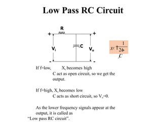
Low Pass RCCircuit
C
X
1
2
f
C
If f=low, Xc becomes high
C act as open circuit, so we get the
output.
If f=high, Xc becomes low
C acts as short circuit, so Vo=0.
As the lower frequency signals appear at the
output, it is called as
“Low pass RC circuit”.
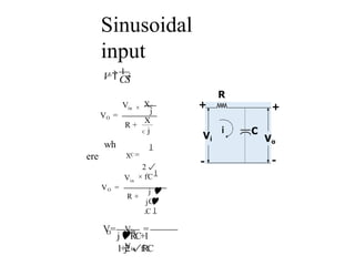
25.
Sinusoidal
input
in
V × XC
O
V=
R +
j
X
C
C
X =
j
1
2
fC
in
V ×
O
V =
R +
1
j
C
1
j
C
wh
ere
O Vin
Vin
V= =
jRC+1
1+j2fRC
CS
o
V
1
i
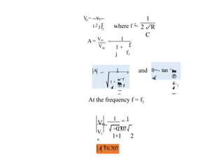
26.
O Vi
n
V =
1+j f
f2
2
where f =
1
2R
C
= 1
A = VO
Vin 1 +
j
f
f2
A =
1 2
1 +
f
f
2
θ=- tan -1
f
f
2
and
At the frequency f = f2
Vi
n
VO=
1 = 1
=0.707
1+1 2
A 0.707
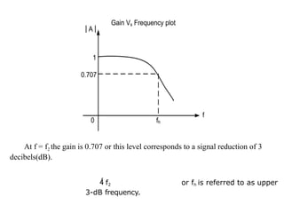
27.
At f =f2 the gain is 0.707 or this level corresponds to a signal reduction of 3
decibels(dB).
f2 or fh is referred to as upper
3-dB frequency.
28.
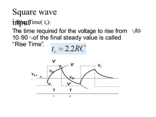
Square wave
input
0
0to
• RiseTime( tr):
The time required for the voltage to rise from
10 90 0
0of the final steady value is called
“Rise Time”.
Vd.c
.
V’
V01
V02
V’ V2
V2
V1
T
1
V’’
T
2
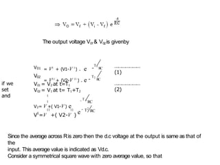
29.
The output voltageV01& V02is givenby
V01
V02
= V1
+ (V1-V 1
) . e -
T1
RC
= V11
+ (V2-V 11
) . e -
T2
RC
…………………
(1)
…………………
(2)
if we
set
and
V01 = V2 at t=T1
V02 = V1 at t= T1+T2
1
1
V2= V +( V1-V) e
11 11
1
-
- T 1
RC
T2
RC
V =V +( V2-V )
e
Since the average across Ris zero then the d.c voltage at the output is same as that of
the
input. This average value is indicated as Vd.c.
Consider a symmetrical square wave with zero average value, so that
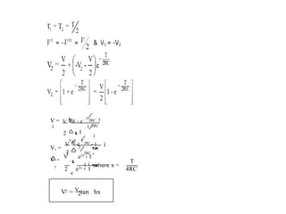
30.
- T
V 1- e
- T
2RC
V =
2 1
+ e
2RC
T
V e
T
2RC - 1
V2 =
2
e
2RC +
1
2
2 e2x
+ 1
V =
V
.
e2x
- 1
where x =
T
4RC
2
V = V tan hx
2
31.
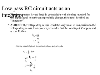
Low pass RCcircuit acts as an
integrator
• The time constant is very large in comparison with the time required for
the input signal to make an appreciable change, the circuit is called an
“Integrator”.
• As RC>>T the voltage drop across C will be very small in comparison to the
voltage drop across R and we may consider that the total input Vi appear and
across R, then
Vi =iR
For low pass RC circuit the output voltage Vo is given by
O
V = 1 i dt
C
O
V = 1
Vi
d
t
C
R
O i
V = 1 V
dt
RC
32.
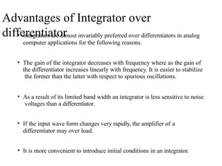
Advantages of Integratorover
differentiator
• Integrators are almost invariably preferred over differentiators in analog
computer applications for the following reasons.
• The gain of the integrator decreases with frequency where as the gain of
the differentiator increases linearly with frequency. It is easier to stabilize
the former than the latter with respect to spurious oscillations.
• As a result of its limited band width an integrator is less sensitive to noise
voltages than a differentiator.
• If the input wave form changes very rapidly, the amplifier of a
differentiator may over load.
• It is more convenient to introduce initial conditions in an integrator.
33.
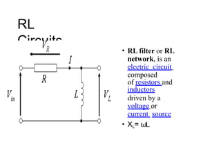
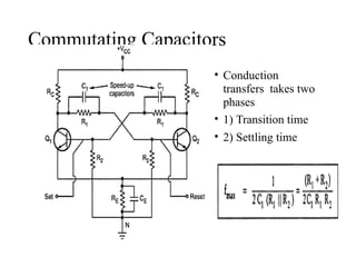
RL
Circuits
• RL filteror RL
network, is an
electric circuit
composed
of resistors and
inductors
driven by a
voltage or
current source
• XL= ωL
Non-Linear Wave Shaping
Definition:The process where by
the form of a signal is changed by
transmission through a non-linear
network is called Non-linear Wave
Shaping.
Types:
i. Clippers.
ii. Clampers.
36.
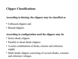
Clipper Classifications
According tobiasing, the clippers may be classified as
• Unbiased clippers and
• Biased clippers.
According to configuration used the clippers may be
• Series diode clippers
• Parallel or shunt diode clippers
• A series combination of diode, resistor and reference
supply
• Multi-diode clippers consisting of several diodes, resistors
and reference voltages
37.
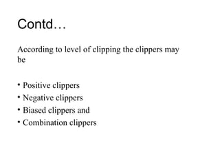
Contd…
According to levelof clipping the clippers may
be
• Positive clippers
• Negative clippers
• Biased clippers and
• Combination clippers
38.
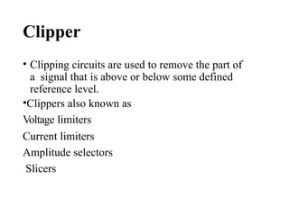
Clipper
• Clipping circuitsare used to remove the part of
a signal that is above or below some defined
reference level.
•Clippers also known as
Voltage limiters
Current limiters
Amplitude selectors
Slicers
40.
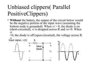
Unbiased clippers( Parallel
PositiveClippers)
•Without the battery, the output of the circuit below would
be the negative portion of the input wave (assuming the
bottom node is grounded). When vi > 0, the diode is on
(short-circuited), vi is dropped across R and vo=0. When
vi
<0, the diode is off (open-circuited), the voltage across R
is
zero and vo=vi.
41.
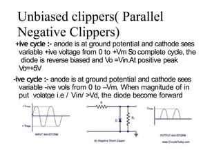
Unbiased clippers( Parallel
NegativeClippers)
+ive cycle :- anode is at ground potential and cathode sees
variable +ive voltage from 0 to +Vm So complete cycle, the
diode is reverse biased and Vo =Vin.At positive peak
Vo=+5V
-ive cycle :- anode is at ground potential and cathode sees
variable -ive vols from 0 to –Vm. When magnitude of in
put volatge i.e / Vin/ >Vd, the diode become forward
biased and hence Vo =-Vd =0.7V
42.
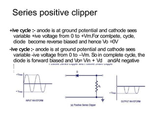
Series positive clipper
+ivecycle :- anode is at ground potential and cathode sees
variable +ive voltage from 0 to +Vm.For comlpete, cycle,
diode become reverse biased and hence Vo =0V
-ive cycle:- anode is at ground potential and cathode sees
variable -ive voltage from 0 to –Vm. So in complete cycle, the
diode is forward biased and Vo= Vin + Vd andAt negative
peak,
Vo= -Vm+ Vd = -
5v
43.
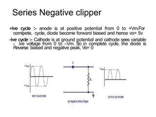
Series Negative clipper
+ivecycle :- anode is at positive potential from 0 to +Vm.For
comlpete, cycle, diode become forward biased and hence vo= 5v
-ive cycle :- Cathode is at ground potential and cathode sees variable
- ive voltage from 0 to –Vm. So in complete cycle, the diode is
Reverse biased and negative peak, Vo= 0
45.
Positive Shunt clippingwith zero
reference Rvoltage
D
Vo
Vi
Transfercharacteristics
equations:
VO=0for Vi>0
VO= Vi for Vi< 0
D–
ON
VO=Vγf
or Vi>Vγ
VO=
Vi for Vi<
Vγ
D–
OFF
[Idea
l]
VO
Vi
VO
Vi
Slope
=1
Vγ Vγ
Input
Input
Output
46.
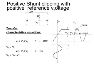
Positive Shunt clippingwith
positive reference vRoltage
D
Vi V
o
Transfer
characteristics equations:
Vi < VR+Vγ D – OFF
VO = Vi
D – ON
Vi > VR+Vγ
VO = VR+Vγ
Input
VR + Vγ VR + Vγ Output
VO
VR VO
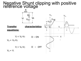
V
i
47.
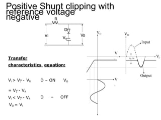
Positive Shunt clippingwith
negative
reference voltage
R
D
VR
Vi Vo
Transfer
characteristics equation:
Vi > Vγ - VR D – ON VO
D – OFF
= Vγ - VR
Vi < Vγ - VR
VO = Vi
VO VO
V
i
Vi
Input
Output
V
i
48.
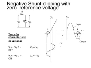
Negative Shunt clippingwith
zero reference voltage
R
Vi Vo
D
Transfer
characteristic
equations:
Vi > -Vγ D –
OFF
VO = Vγ
Vi < -Vγ D –
ON
VO = -Vγ
-Vγ -Vγ
VO
VO
V
i
V
i
Input
Output
49.
Negative Shunt clippingwith positive
reference voltage
R
D
VR
Vi Vo
Transfer characteristics
equations:
D – ON
Vi < VR-Vγ
VO = VR-Vγ
Vi > VR-Vγ D – OFF
VO = Vi
VR - Vγ
VO
V
i
V
i
VO
DOFF
DON
50.
Negative Shunt clippingwith
negative reference voltage
R
D
VR
Vi Vo
Transfer characteristic
equations:
D – ON VO
Vi < -( Vγ + VR)
= -( Vγ + VR)
Vi < -( Vγ + VR) D – OFF VO = Vi
VO VO
V
i
V
i
- (Vγ +
VR
Input
51.
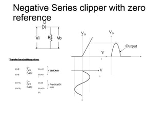
Negative Series clipperwith zero
reference
R
Vi Vo
D
Transfercharacteristicequations:
Vi<
0
D–
OFF
VO=0
IdealDiode
Vi>
0
D–ON
VO=V
i
Vi<Vγ
D–
OFF
VO=
0
PracticalDi
ode
Vi>Vγ
D–ON VO=Vi-
Vγ
VO
VO
V
i
V
i
Output
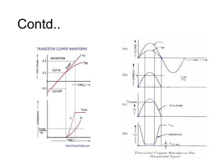
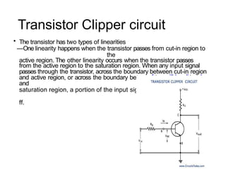
Transistor Clipper circuit
waveformwill be clipped
o
• The transistor has two types of linearities
—One linearity happens when the transistor passes from cut-in region to
the
active region. The other linearity occurs when the transistor passes
from the active region to the saturation region. When any input signal
passes through the transistor, across the boundary between cut-in region
and active region, or across the boundary between the active region
and
saturation region, a portion of the input signal
ff.
55.
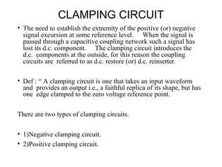
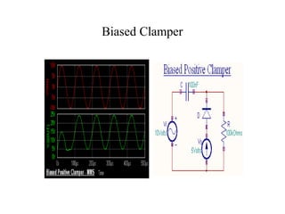
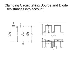
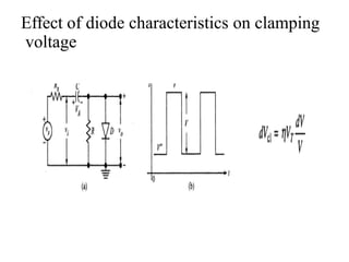
CLAMPING CIRCUIT
• Theneed to establish the extremity of the positive (or) negative
signal excursion at some reference level. When the signal is
passed through a capacitive coupling network such a signal has
lost its d.c. component. The clamping circuit introduces the
d.c. components at the outside, for this reason the coupling
circuits are referred to as d.c. restore (or) d.c. reinserter.
• Def : “ A clamping circuit is one that takes an input waveform
and provides an output i.e., a faithful replica of its shape, but has
one edge clamped to the zero voltage reference point.
There are two types of clamping circuits.
• 1)Negative clamping circuit.
• 2)Positive clamping circuit.
56.
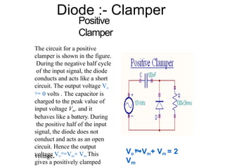
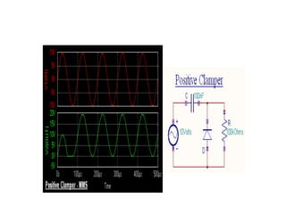
Diode :- Clamper
Positive
Clamper
Thecircuit for a positive
clamper is shown in the figure.
During the negative half cycle
of the input signal, the diode
conducts and acts like a short
circuit. The output voltage Vo
0 volts . The capacitor is
charged to the peak value of
input voltage Vm. and it
behaves like a battery. During
the positive half of the input
signal, the diode does not
conduct and acts as an open
circuit. Hence the output
voltage VoVm+ Vm This
gives a positively clamped
voltage.
VoVm+ Vm = 2
Vm
58.
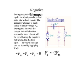
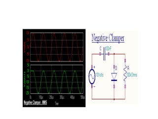
Negative
Clamper
During the positivehalf
cycle the diode conducts and
acts like a short circuit. The
capacitor charges to peak
value of input voltage Vm.
During this interval the
output Vo which is taken
across the short circuit will
be zero During the negative
half cycle, the diode is
open. The output voltage
can be found by applying
KVL.
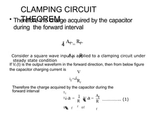
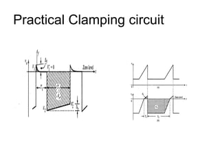
CLAMPING CIRCUIT
THEOREM
• Thereforethe charge acquired by the capacitor
during the forward interval
Af =
Rf
Ar R
Consider a square wave input is applied to a clamping circuit under
steady state condition
If Vf (t) is the output waveform in the forward direction, then from below figure
the capacitor charging current is
V
if
= f
Rf
Therefore the charge acquired by the capacitor during the
forward interval
i dt = V dt =
Af
R
f
T1
T1
f
1
R
f
f
0 0
…………….. (1)
62.
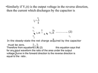
•Similarly if Vf(t) is the output voltage in the reverse direction,
then the current which discharges by the capacitor is
1 Ar
T2
T2
ir dt =
R Vr dt
=
R
…………….. (2)
T1 T2
In the steady-state the net charge acquired by the capacitor
must be zero.
Therefore from equation (1) & (2) this equation says that
for any input waveform the ratio of the area under the output
voltage curve in the forward direction to the reverse direction is
equal to the ratio .
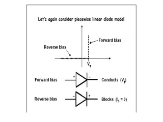
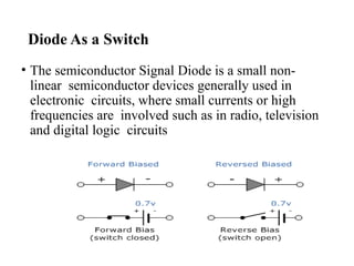
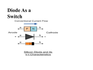
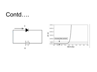
Diode As aSwitch
• The semiconductor Signal Diode is a small non-
linear semiconductor devices generally used in
electronic circuits, where small currents or high
frequencies are involved such as in radio, television
and digital logic circuits
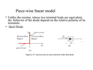
• Unlike theresistor, whose two terminal leads are equivalent,
the behavior of the diode depend on the relative polarity of its
terminals.
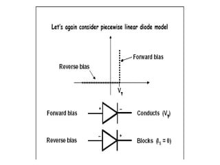
• Ideal Diode
•
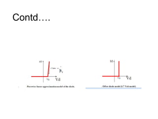
Piece-wise linear model
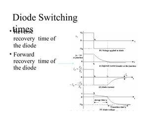
Contd…
• As longas the voltage Vi = VF till t1, the diode is ON. The
forward resistance of the diode being negligible when compared to RL,
therefore If= Vf/R. At t = t1, the polarity of Vi is abruptly reversed, i.e.Vi = -
VR and Ir = - Vr/R until t = t2 at which time minority carrier density pn at x
= 0 has reached the equilibrium value pn0.
• At t = t2 the charge carriers have been swept, the polarity of the diode
voltage reverses, the diode current starts to decrease. The time duration, t1 to
t2, during which period the stored minority charge becomes zero is called the
storage time ts. The time interval from t2 to the instant that the diode has
recovered (V = -VR) is called the transition time,tt. The sum total of the
storage time,ts and the transition time,tt is called the reverse recovery time of
the diode, trr.
• trr = ts + tt
76.
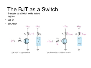
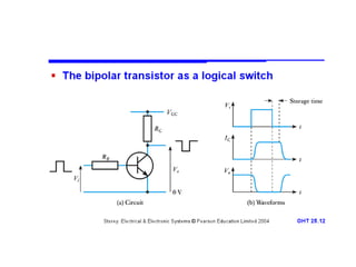
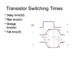
The BJT asa Switch
• Transistor as a Switch works in two
regions
• Cut off
• Saturation
Contd..
• Delay Time,td : It is the time taken for the collector current to reach from its initial
value to 10% of its final value If the rise of the collector current is linear, the time
required to rise to 10%IC(sat) is 1/8 the time required for the current to rise from
10% to 90% IC(sat). where tr is the rise time
• Rise Time,tr : It is the time taken for the collector current to reach from 10% of its
final value to 90% of its final value. However, because of the stored charges, the
current remains unaltered for sometime interval ts1 and then begins to fall. The time
taken for this current to fall from its initial value at ts1 to 90% of its initial value is
ts2. The sum of these ts1 and ts2 is approximately ts1 and is called the storage time.
• Storage time, ts : It is the time taken for the collector current to fall from its initial
value to 90% of its initial value.
• . Fall time, tf : It is the time taken for the collector current to fall from 90% of its
initial value to 10% of its Initial value.
• Ton= td+tr
• Toff= ts+tf
80.
Breakdown mechanisms in
BJTs
•The breakdown voltage of a BJTalso depends on the chosen circuit
configuration:
• In a common base mode (i.e. operation where the base is grounded and
forms the common electrode between the emitter-base input and collector-
base output of the device) the breakdown resembles that of a p-n diode.
• In a common emitter mode (i.e. operation where the emitter is grounded and
forms the common electrode between the base-emitter input and the
collector- emitter output of the device) the transistor action further influences
the I-V characteristics and breakdown voltage.
• Avalanche breakdown of the base-collector junction is further influenced by
transistor action in common-emitter mode of operation, since the holes
generated by impact ionization are pulled back into the base region which
results in an additional base current. This additional base current causes an
even larger additional flow of electrons through the base and into the
collector due to the current gain of the BJT
.This larger flow of electrons in
the base collector junction causes an even larger generation of electron-hole
pairs.
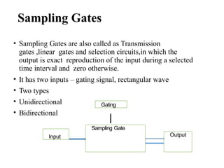
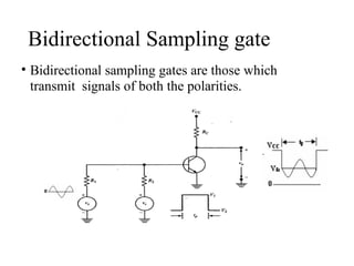
Sampling Gates
• SamplingGates are also called as Transmission
gates ,linear gates and selection circuits,in which the
output is exact reproduction of the input during a selected
time interval and zero otherwise.
• It has two inputs – gating signal, rectangular wave
• Two types
• Unidirectional
• Bidirectional
Gating
Input
Sampling Gate
Output
83.
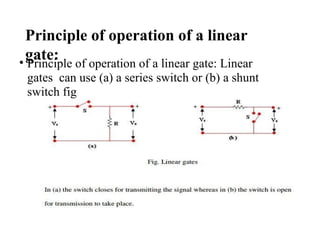
Principle of operationof a linear
gate:
• Principle of operation of a linear gate: Linear
gates can use (a) a series switch or (b) a shunt
switch fig
84.
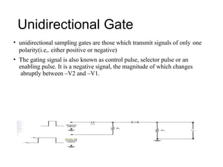
Unidirectional Gate
• unidirectionalsampling gates are those which transmit signals of only one
polarity(i.e,. either positive or negative)
• The gating signal is also known as control pulse, selector pulse or an
enabling pulse. It is a negative signal, the magnitude of which changes
abruptly between –V2 and –V1.
85.
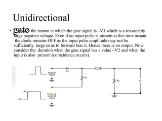
Unidirectional
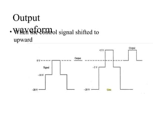
gate
• Consider theinstant at which the gate signal is –V1 which is a reasonably
large negative voltage. Even if an input pulse is present at this time instant,
the diode remains OFF as the input pulse amplitude may not be
sufficiently large so as to forward bias it. Hence there is no output. Now
consider the duration when the gate signal has a value –V2 and when the
input is also present (coincidence occurs).
pedestal
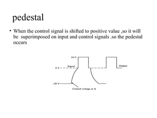
• When thecontrol signal is shifted to positive value ,so it will
be superimposed on input and control signals .so the pedestal
occurs
88.
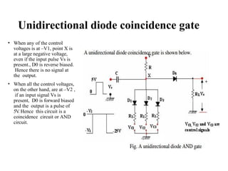
Unidirectional diode coincidencegate
• When any of the control
voltages is at –V1, point X is
at a large negative voltage,
even if the input pulse Vs is
present., D0 is reverse biased.
Hence there is no signal at
the output.
• When all the control voltages,
on the other hand, are at –V2 ,
if an input signal Vs is
present, D0 is forward biased
and the output is a pulse of
5V
. Hence this circuit is a
coincidence circuit or AND
circuit.
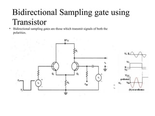
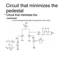
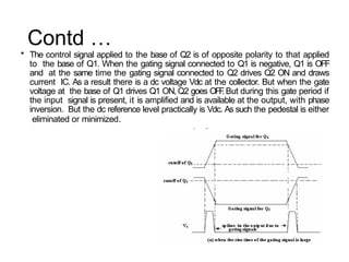
Contd …
• Thecontrol signal applied to the base of Q2 is of opposite polarity to that applied
to the base of Q1. When the gating signal connected to Q1 is negative, Q1 is OFF
and at the same time the gating signal connected to Q2 drives Q2 ON and draws
current IC. As a result there is a dc voltage Vdc at the collector. But when the gate
voltage at the base of Q1 drives Q1 ON, Q2 goes OFF
. But during this gate period if
the input signal is present, it is amplified and is available at the output, with phase
inversion. But the dc reference level practically is Vdc. As such the pedestal is either
eliminated or minimized.
93.
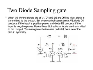
Two Diode Samplinggate
• When the control signals are at V1, D1 and D2 are OFF
,no input signal is
transmitted to the output. But when control signals are at V2, diode D1
conducts if the input is positive pulses and diode D2 conducts if the
input is negative pulses. Hence these bidirectional inputs are transmitted
to the output. This arrangement eliminates pedestal, because of the
circuit symmetry.
94.
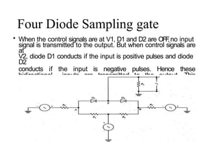
Four Diode Samplinggate
• When the control signals are at V1, D1 and D2 are OFF
,no input
signal is transmitted to the output. But when control signals are
at
V2, diode D1 conducts if the input is positive pulses and diode
D2
conducts if the input is negative pulses. Hence these
bidirectional inputs are transmitted to the output. This
arrangement eliminates pedestal, because of the circuit
symmetry.
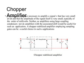
Chopper
Amplifier
• Sometimes itbecomes necessary to amplify a signal v that has very small
dv/dt and that the amplitude of the signal itself is very small, typically of
the order of millivolts. Neither, ac amplifiers using large coupling
condensers nor dc amplifiers with the associated drift would be useful for
such an application. A chopper stabilized amplifier employing sampling
gates can be a useful choice in such a applications
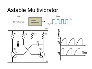
Multivibrators
• Multivibrator –A circuit designed to have zero, one, or
two stable output states.
• There are three types of multivibrators.
• Astable (or Free-Running Multivibrator)
• Monostable (or One-Shot)
• Bistable (or Flip-Flop)
99.
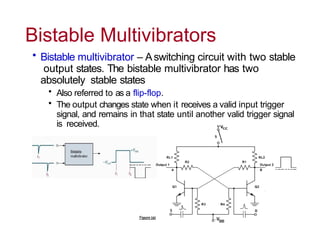
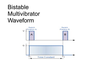
Bistable Multivibrators
• Bistablemultivibrator – Aswitching circuit with two stable
output states. The bistable multivibrator has two
absolutely stable states
• Also referred to as a flip-flop.
• The output changes state when it receives a valid input trigger
signal, and remains in that state until another valid trigger signal
is received.
Monostable Multivibrator
• Multivibratorshave two different electrical states, an output “HIGH” state and an
output “LOW” state giving them either a stable or quasi-stable state depending upon
the type of multivibrator. One such type of a two state pulse generator configuration
are called Monostable Multivibrators.
• Monostable Multivibrators have only ONE stable state (hence their name: “Mono”), and
produce a single output pulse when it is triggered externally. Monostable Multivibrators only
return back to their first original and stable state after a period of time determined by the
time constant of the RC coupled circuit.
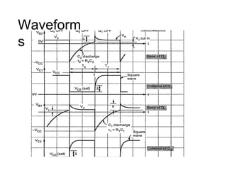
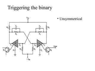
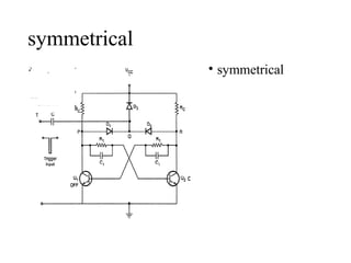
Triggering the binary
•Two types of triggering
• 1) Symmetrical 2) Unsymmetrical
• In un symmetrical triggering, two triggers are required. One
to set the circuit in particular stable state and other is to
reset
• In Symmetrical triggering , uses only one trigger pulse input
to the any of the one transistor
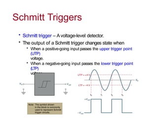
Schmitt Triggers
• Schmitttrigger – Avoltage-level detector.
• The output of a Schmitt trigger changes state when
• When a positive-going input passes the upper trigger point
(UTP)
voltage.
• When a negative-going input passes the lower trigger point
(LTP)
voltage.
110.
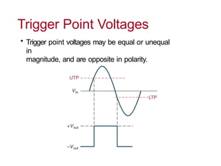
Trigger Point Voltages
•Trigger point voltages may be equal or unequal
in
magnitude, and are opposite in polarity.
111.
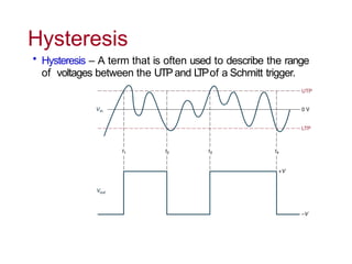
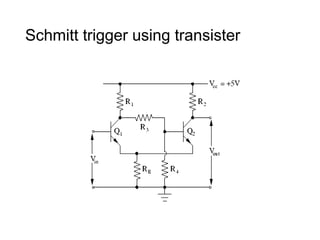
Hysteresis
• Hysteresis –A term that is often used to describe the range
of voltages between the UTPand L
TPof a Schmitt trigger.
• Assume NPNtransistor with
• Let
vardhaman
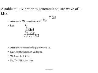
Astable multivibrator to generate a square wave of 1
kHz:
25
h fe
Ic
5mA
Vcc
12V
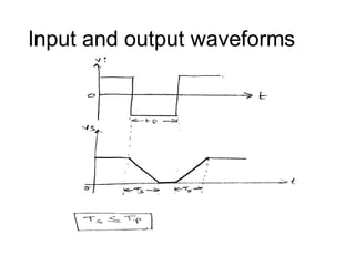
T1T2 T/2
• Assume symmetrical square wave i.e.
• Neglect the junction voltages.
• We have f= 1 kHz
• So, T=1/1kHz = 1ms
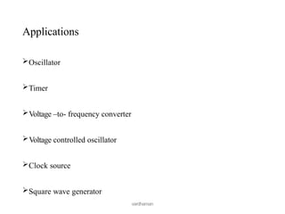
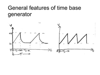
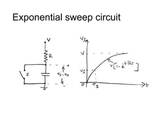
Time base generator
Constantcurrent charging
Acapacitor is charged with constant current source.
As it charged with constant current, it is charged linearly.
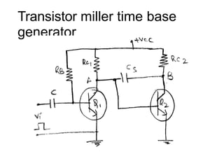
Miller circuit:
Integrator is used to convert a step waveform to ramp
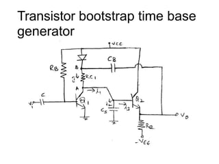
waveform. Bootstrap circuits
Aconstant current source is obtained by maintaining nearly
constant
voltage across the fixed resistor in series with capacitor.
Compensating network is used to improve the linearity of
bootstrap and
miller time base generator
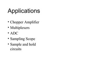
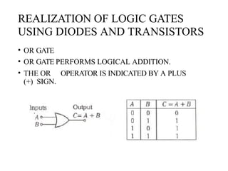
REALIZATION OF LOGICGATES
USING DIODES AND TRANSISTORS
• OR GATE
• OR GATE PERFORMS LOGICAL ADDITION.
• THE OR OPERATOR IS INDICATED BY A PLUS
(+) SIGN.
128.
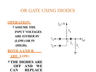
OR GATE USINGDIODES
OPERATION:
ASSUME THE
INPUT VOLTAGES
ARE EITHER 0V
(LOW) OR 5V
(HIGH).
BOTH AAND B
ARE LOW:
THE DIODES ARE
OFF AND WE
CAN REPLACE
129.
Contd.
A IS LOWAND B IS HIGH:
• WHEN A IS LOW THE CORRESPONDING DIODE WILL BE OFF
AND, B IS HIGH SO THE DIODE CORRESPONDS TO THE INPUT B
WILL BE ON.
• NOW WE CAN REPLACE THE ON DIODE BY THE SHORT CIRCUIT
EQUIVALENT AND THE OUTPUT C=5V.
• B IS LOW AND A IS HIGH:
• WHEN B IS LOW THE CORRESPONDING DIODE WILL BE OFFAND,
A IS HIGH SO THE DIODE CORRESPONDS TO THE INPUT A WILL
BE ON.
• NOW WE CAN REPLACE THE ON DIODE BY THE SHORT CIRCUIT
EQUIVALENT AND THE OUTPUT C=5V.
• BOTH AAND B ARE HIGH:
• WHEN BOTH THE INPUTS ARE HIGH BOTH THE DIODES WILL BE
ON AND THE OUTPUT C=5V.
130.
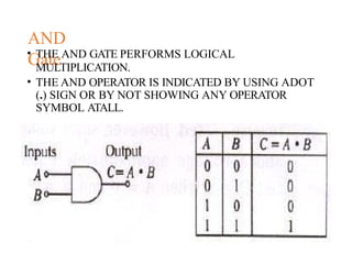
AND
Gate
• THE ANDGATE PERFORMS LOGICAL
MULTIPLICATION.
• THE AND OPERATOR IS INDICATED BY USING ADOT
(.) SIGN OR BY NOT SHOWING ANY OPERATOR
SYMBOL ATALL.
131.
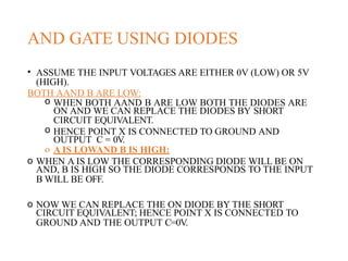
AND GATE USINGDIODES
• ASSUME THE INPUT VOLTAGES ARE EITHER 0V (LOW) OR 5V
(HIGH).
BOTH AAND B ARE LOW:
o WHEN BOTH AAND B ARE LOW BOTH THE DIODES ARE
ON AND WE CAN REPLACE THE DIODES BY SHORT
CIRCUIT EQUIVALENT.
o HENCE POINT X IS CONNECTED TO GROUND AND
OUTPUT C = 0V.
o A IS LOWAND B IS HIGH:
o WHEN A IS LOW THE CORRESPONDING DIODE WILL BE ON
AND, B IS HIGH SO THE DIODE CORRESPONDS TO THE INPUT
B WILL BE OFF.
o NOW WE CAN REPLACE THE ON DIODE BY THE SHORT
CIRCUIT EQUIVALENT; HENCE POINT X IS CONNECTED TO
GROUND AND THE OUTPUT C=0V.
132.
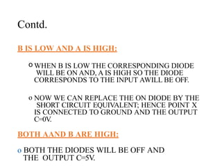
Contd.
B IS LOWAND A IS HIGH:
o WHEN B IS LOW THE CORRESPONDING DIODE
WILL BE ON AND, A IS HIGH SO THE DIODE
CORRESPONDS TO THE INPUT AWILL BE OFF.
o NOW WE CAN REPLACE THE ON DIODE BY THE
SHORT CIRCUIT EQUIVALENT; HENCE POINT X
IS CONNECTED TO GROUND AND THE OUTPUT
C=0V.
BOTH AAND B ARE HIGH:
o BOTH THE DIODES WILL BE OFF AND
THE OUTPUT C=5V.
133.
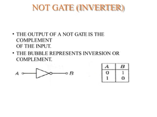
NOT GATE (INVERTER)
•THE OUTPUT OF A NOT GATE IS THE
COMPLEMENT
OF THE INPUT.
• THE BUBBLE REPRESENTS INVERSION OR
COMPLEMENT.
134.
REALIZATION OF NOTGATE
USING TRANSISTOR
A IS HIGH:
o When +5v is applied to a, the
transistor will be fully on.
o So maximum
collector current will
flow and vcc
=icr, making vc or voltage
at
point b as zero. [Recall ce
loop kvl: vc=vcc-icr].
o A IS LOW:
When 0v is applied to a,
the transistor will be cut-
off.
So ic=0ma and vc or
voltage
at point b is equal to vcc.
135.
Logic Families
Vocabulary
TTL (TransistorTransistor Logic) Integrated-circuit technology that uses
the bipolar transistor as the principal circuit element.
CMOS (Complimentary Metal Oxide Semiconductor) Integrated-circuit
technology that uses the field-effect transistor as the principal circuit element.
ECL (Emitter Coupled Logic) Integrated-circuit technology that uses the
bipolar transistors configured as a differential amplifier. This eliminates
saturation and improves speed but uses more power than other families.
136.
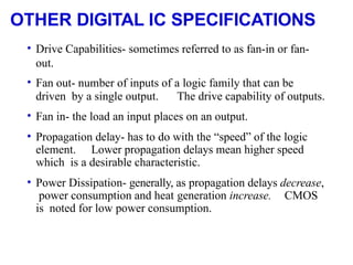
OTHER DIGITAL ICSPECIFICATIONS
• Drive Capabilities- sometimes referred to as fan-in or fan-
out.
• Fan out- number of inputs of a logic family that can be
driven by a single output. The drive capability of outputs.
• Fan in- the load an input places on an output.
• Propagation delay- has to do with the “speed” of the logic
element. Lower propagation delays mean higher speed
which is a desirable characteristic.
• Power Dissipation- generally, as propagation delays decrease,
power consumption and heat generation increase. CMOS
is noted for low power consumption.
137.
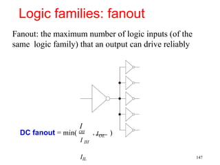
Fanout: the maximumnumber of logic inputs (of the
same logic family) that an output can drive reliably
Logic families: fanout
I
DC fanout = min( OH , )
I IH
IIL
IOL
147
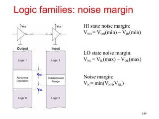
Logic families: noisemargin
VNH
VNL
HI state noise margin:
VNH = VOH(min) – VIH(min)
LO state noise margin:
VNL = VIL(max) – VOL(max)
Noise margin:
VN = min(VNH,VNL)
149
140.
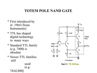
TOTEM POLE NANDGATE
• First introduced by
in 1964 (Texas
Instruments)
• TTL has shaped
digital technology
in many ways
• Standard TTL family
(e.g. 7400) is
obsolete
• Newer TTL families
still
used
(e.g.
74ALS00)
141.
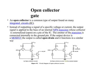
Open collector
gate
• Anopen collector is a common type of output found on many
integrated circuits (IC).
• Instead of outputting a signal of a specific voltage or current, the output
signal is applied to the base of an internal NPN transistor whose collector
is externalized (open) on a pin of the IC. The emitter of the transistor is
connected internally to the ground pin. If the output device is
a MOSFET the output is called open drain and it functions in a similar
way.
142.
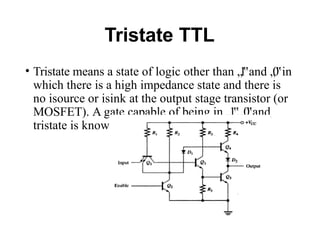
Tristate TTL
• Tristatemeans a state of logic other than „
1
‟and „
0
‟in
which there is a high impedance state and there is
no isource or isink at the output stage transistor (or
MOSFET). A gate capable of being in „1,
‟„
0
‟and
tristate is known as tristate
gate
143.
Direct-coupled transistor
logic (DCTL)
•Direct-coupled transistor logic (DCTL) is similar to
resistor–
transistor logic (RTL) but the input transistor bases are connected
directly to the collector outputs without any base resistors
.
Consequently, DCTL gates have fewer components, are
more
economical, and are simpler to fabricate onto integrated circuits
than RTL gates. Unfortunately, DCTL has much smaller signal
levels, has more susceptibility to ground noise, and requires
matched transistor characteristics. The transistors are also heavily
overdriven; that is a good feature in that it reduces the saturation
voltage of the output transistors, but it also slows the circuit down
due to a high stored charge in the base.[1] Gate fan-out is limited
due to "current hogging": if the transistor base-emitter voltages
(VBE) are not well matched, then the base-emitter junction of one
transistor may conduct most of the input drive current at such a
low base-emitter voltage that other input transistors fail to turn on
144.
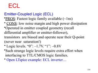
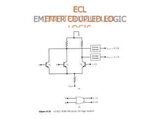
ECL
Emitter-Coupled Logic (ECL)
•PROS:Fastest logic family available (~1ns)
• CONS: low noise margin and high power dissipation
•Operated in emitter coupled geometry (recall
differential amplifier or emitter-follower),
transistors are biased and operate near their Q-point
(never near saturation!)
• Logic levels. “0”: –1.7V. “1”: –0.8V
•Such strange logic levels require extra effort when
interfacing to TTL/CMOS logic families.
• Open LTspice example: ECL inverter…
154
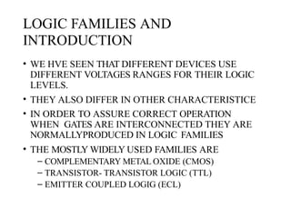
LOGIC FAMILIES AND
INTRODUCTION
•WE HVE SEEN THAT DIFFERENT DEVICES USE
DIFFERENT VOLTAGES RANGES FOR THEIR LOGIC
LEVELS.
• THEY ALSO DIFFER IN OTHER CHARACTERISTICE
• IN ORDER TO ASSURE CORRECT OPERATION
WHEN GATES ARE INTERCONNECTED THEY ARE
NORMALLYPRODUCED IN LOGIC FAMILIES
• THE MOSTLY WIDELY USED FAMILIES ARE
– COMPLEMENTARY METAL OXIDE (CMOS)
– TRANSISTOR- TRANSISTOR LOGIC (TTL)
– EMITTER COUPLED LOGIG (ECL)

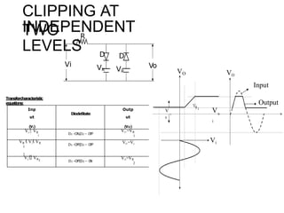
![Positive Shunt clipping with zero
reference Rvoltage
D
Vo
Vi
Transfercharacteristics
equations:
VO=0for Vi>0
VO= Vi for Vi< 0
D–
ON
VO=Vγf
or Vi>Vγ
VO=
Vi for Vi<
Vγ
D–
OFF
[Idea
l]
VO
Vi
VO
Vi
Slope
=1
Vγ Vγ
Input
Input
Output](https://image.slidesharecdn.com/pdc-250718062917-bd2cc17c/85/pulse-and-digital-circuits-pulse-and-digital-circuits-45-320.jpg)


![REALIZATION OF NOT GATE
USING TRANSISTOR
A IS HIGH:
o When +5v is applied to a, the
transistor will be fully on.
o So maximum
collector current will
flow and vcc
=icr, making vc or voltage
at
point b as zero. [Recall ce
loop kvl: vc=vcc-icr].
o A IS LOW:
When 0v is applied to a,
the transistor will be cut-
off.
So ic=0ma and vc or
voltage
at point b is equal to vcc.](https://image.slidesharecdn.com/pdc-250718062917-bd2cc17c/85/pulse-and-digital-circuits-pulse-and-digital-circuits-134-320.jpg)

![Direct-coupled transistor
logic (DCTL)
• Direct-coupled transistor logic (DCTL) is similar to
resistor–
transistor logic (RTL) but the input transistor bases are connected
directly to the collector outputs without any base resistors
.
Consequently, DCTL gates have fewer components, are
more
economical, and are simpler to fabricate onto integrated circuits
than RTL gates. Unfortunately, DCTL has much smaller signal
levels, has more susceptibility to ground noise, and requires
matched transistor characteristics. The transistors are also heavily
overdriven; that is a good feature in that it reduces the saturation
voltage of the output transistors, but it also slows the circuit down
due to a high stored charge in the base.[1] Gate fan-out is limited
due to "current hogging": if the transistor base-emitter voltages
(VBE) are not well matched, then the base-emitter junction of one
transistor may conduct most of the input drive current at such a
low base-emitter voltage that other input transistors fail to turn on](https://image.slidesharecdn.com/pdc-250718062917-bd2cc17c/85/pulse-and-digital-circuits-pulse-and-digital-circuits-143-320.jpg)