This document provides an overview and table of contents for the book "RF Microelectronics" by Behzad Razavi. It describes the book as focusing on radio frequency integrated circuit design and analysis. The preface outlines the book's goal of explaining RF analysis techniques and their predictive design capabilities. The table of contents lists the book's 9 chapters which cover topics such as basic RF concepts, communication systems, transceiver architectures, low-noise amplifiers, mixers, passive components, oscillators, and phase-locked loops.


![CHAPTER
1
INTRODUCTION TO RF AND
WIRELESS TECHNOLOGY
Compare two RF transceivers designed for cell phones:
“A 2.7-V GSM RF Transceiver IC” [1] (published in 1997)
“A Single-Chip 10-Band WCDMA/HSDPA 4-Band GSM/EDGE SAW-
Less CMOS Receiver with DigRF 3G Interface and 190-dBm IIP2” [2]
(published in 2009)
Why is the latter much more complex than the former? Does the latter have a higher perfor-
mance or only greater functionality? Which one costs more? Which one consumes a higher
power? What do all the acronyms GSM, WCDMA, HSDPA, EDGE, SAW, and IIP2 mean?
Why do we care?
The field of RF communication has grown rapidly over the past two decades, reaching
far into our lives and livelihood. Our cell phones serve as an encyclopedia, a shopping
terminus, a GPS guide, a weather monitor, and a telephone—all thanks to their wireless
communication devices. We can now measure a patient’s brain or heart activity and transmit
the results wirelessly, allowing the patient to move around untethered. We use RF devices
to track merchandise, pets, cattle, children, and convicts.
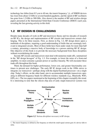
1.1 A WIRELESS WORLD
Wireless communication has become almost as ubiquitous as electricity; our refrigera-
tors and ovens may not have a wireless device at this time, but it is envisioned that our
homes will eventually incorporate a wireless network that controls every device and appli-
ance. High-speed wireless links will allow seamless connections among our laptops, digital
cameras, camcorders, cell phones, printers, TVs, microwave ovens, etc. Today’s WiFi and
Bluetooth connections are simple examples of such links.
How did wireless communication take over the world? A confluence of factors has
contributed to this explosive growth. The principal reason for the popularity of wireless
1](https://image.slidesharecdn.com/rfmicroelectronicsrazavi-230814101614-71259b59/85/RF-MICROELECTRONICS_Razavi-pdf-26-320.jpg)
![2 Chap. 1. Introduction to RF and Wireless Technology
communication is the ever-decreasing cost of electronics. Today’s cell phones cost about
the same as those a decade ago but they offer many more functions and features: many
frequency bands and communication modes, WiFi, Bluetooth, GPS, computing, storage,
a digital camera, and a user-friendly interface. This affordability finds its roots in inte-
gration, i.e., how much functionality can be placed on a single chip—or, rather, how few
components are left off-chip. The integration, in turn, owes its steady rise to (1) the scaling
of VLSI processes, particularly, CMOS technology, and (2) innovations in RF architectures,
circuits, and devices.
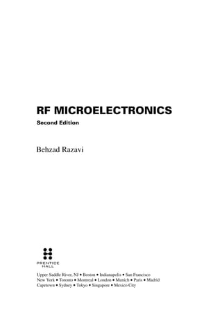
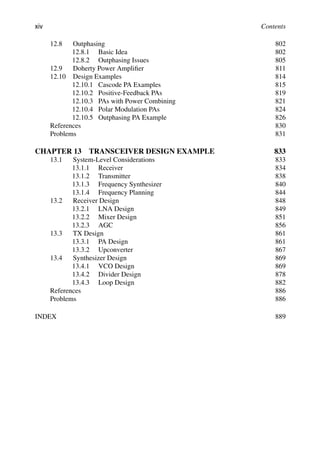
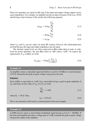
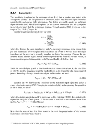
Along with higher integration levels, the performance of RF circuits has also improved.
For example, the power consumption necessary for a given function has decreased and the
speed of RF circuits has increased. Figure 1.1 illustrates some of the trends in RF integrated
circuits (ICs) and technology for the past two decades. The minimum feature size of CMOS
1000
100
10
1
88 90 92 94 96 98 00 02 04 06 08 10
Year
T
Oscillation
Frequency
and
f
(GHz)
0.5
um
0.35
um
0.25
um
0.18
um
0.13
um
90
nm
Osc. Freq.
f T
40
nm
65
nm
[3] [4]
[5]
[6]
[7]
[8] [9]
[10]
88 90 92 94 96 98 00 02 04 06 08 10
Year
10
20
30
40
50
60
70
Number
of
RF
and
Wireless
Papers
at
ISSCC
Figure 1.1 Trends in RF circuits and technology.](https://image.slidesharecdn.com/rfmicroelectronicsrazavi-230814101614-71259b59/85/RF-MICROELECTRONICS_Razavi-pdf-27-320.jpg)
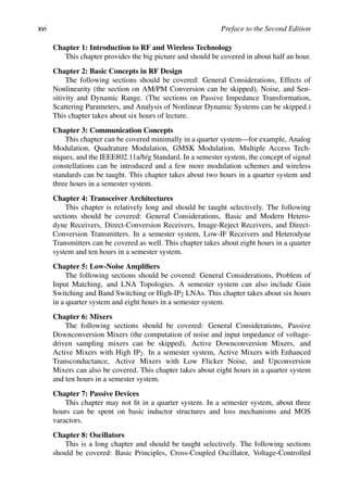
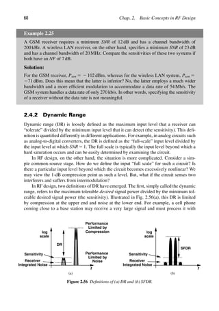
![4 Chap. 1. Introduction to RF and Wireless Technology
Noise Power
Linearity
Gain
Supply
Voltage
Frequency
Figure 1.3 RF design hexagon.
dominated by the digital baseband processor, allowing RF and analog designers some lat-
itude in the choice of their circuit and device topologies. In today’s designs, however, the
multiple transceivers tend to occupy a larger area than the baseband processor, requiring
that RF and analog sections be designed with much care about their area consumption.
For example, while on-chip spiral inductors (which have a large footprint) were utilized in
abundance in older systems, they are now used only sparingly.
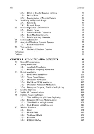
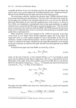
1.3 THE BIG PICTURE
The objective of an RF transceiver is to transmit and receive information. We envision
that the transmitter (TX) somehow processes the voice or data signal and applies the result
to the antenna [Fig. 1.4(a)]. Similarly, the receiver (RX) senses the signal picked up by
the antenna and processes it so as to reconstruct the original voice or data information.
Each black box in Fig. 1.4(a) contains a great many functions, but we can readily make
two observations: (1) the TX must drive the antenna with a high power level so that the
transmitted signal is strong enough to reach far distances, and (2) the RX may sense a
small signal (e.g., when a cell phone is used in the basement of a building) and must first
amplify the signal with low noise. We now architect our transceiver as shown in Fig. 1.4(b),
where the signal to be transmitted is first applied to a “modulator” or “upconverter” so that
its center frequency goes from zero to, say, fc 5 2.4 GHz. The result drives the antenna
through a “power amplifier” (PA). On the receiver side, the signal is sensed by a “low-
noise amplifier” (LNA) and subsequently by a “downconverter” or “demodulator” (also
known as a “detector”).
The upconversion and downconversion paths in Fig. 1.4(b) are driven by an oscillator,
which itself is controlled by a “frequency synthesizer.” Figure 1.4(c) shows the overall
transceiver.2
The system looks deceptively simple, but we will need the next 900 pages to
cover its RF sections. And perhaps another 900 pages to cover the analog-to-digital and
digital-to-analog converters.
2. In some cases, the modulator and the upconverter are one and the same. In some other cases, the modula-
tion is performed in the digital domain before upconversion. Most receivers demodulate and detect the signal
digitally, requiring only a downconverter in the analog domain.](https://image.slidesharecdn.com/rfmicroelectronicsrazavi-230814101614-71259b59/85/RF-MICROELECTRONICS_Razavi-pdf-29-320.jpg)
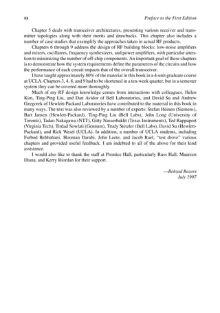
![References 5
?
Transmitter (TX) Receiver (RX)
?
Voice or
Data
Reconstructed
Voice or Data
Power
Amplifier
Upconverter or
Modulator
Voice or
Data
0 f
Amplifier
Low−Noise
f
fc
Downconverter or
Demodulator
Reconstructed
Voice or Data
f
fc 0 f
Downconverter or
Demodulator
LNA
PA
Upconverter or
Modulator
Frequency
Synthesizer
Oscillator
Converter
Analog−to−Digital
Converter
Digital−to−Analog
Digital
Baseband
Processor
(a)
(b)
(c)
Figure 1.4 (a) Simple view of RF communication, (b) more complete view, (c) generic RF
transceiver.
REFERENCES
[1] T. Yamawaki et al., “A 2.7-V GSM RF Transceiver IC,” IEEE J. Solid-State Circuits, vol. 32,
pp. 2089–2096, Dec. 1997.
[2] D. Kaczman et al., “A Single-Chip 10-Band WCDMA/HSDPA 4-Band GSM/EDGE SAW-
less CMOS Receiver with DigRF 3G Interface and 190-dBm IIP2,” IEEE J. Solid-State
Circuits, vol. 44, pp. 718–739, March 2009.
[3] M. Banu, “MOS Oscillators with Multi-Decade Tuning Range and Gigahertz Maximum
Speed,” IEEE J. Solid-State Circuits, vol. 23, pp. 474–479, April 1988.
[4] B. Razavi et al., “A 3-GHz 25-mW CMOS Phase-Locked Loop,” Dig. of Symposium on VLSI
Circuits, pp. 131–132, June 1994.](https://image.slidesharecdn.com/rfmicroelectronicsrazavi-230814101614-71259b59/85/RF-MICROELECTRONICS_Razavi-pdf-30-320.jpg)
![6 Chap. 1. Introduction to RF and Wireless Technology
[5] M. Soyuer et al., “A 3-V 4-GHz nMOS Voltage-Controlled Oscillator with Integrated
Resonator,” IEEE J. Solid-State Circuits, vol. 31, pp. 2042–2045, Dec. 1996.
[6] B. Kleveland et al., “Monolithic CMOS Distributed Amplifier and Oscillator,” ISSCC Dig.
Tech. Papers, pp. 70–71, Feb. 1999.
[7] H. Wang, “A 50-GHz VCO in 0.25-μm CMOS,” ISSCC Dig. Tech. Papers, pp. 372–373,
Feb. 2001.
[8] L. Franca-Neto, R. Bishop, and B. Bloechel, “64 GHz and 100 GHz VCOs in 90 nm CMOS
Using Optimum Pumping Method,” ISSCC Dig. Tech. Papers, pp. 444–445, Feb. 2004.
[9] E. Seok et al., “A 410GHz CMOS Push-Push Oscillator with an On-Chip Patch Antenna”
ISSCC Dig. Tech. Papers, pp. 472–473, Feb. 2008.
[10] B. Razavi, “A 300-GHz Fundamental Oscillator in 65-nm CMOS Technology,” Symposium
on VLSI Circuits Dig. Of Tech. Papers, pp. 113–114, June 2010.](https://image.slidesharecdn.com/rfmicroelectronicsrazavi-230814101614-71259b59/85/RF-MICROELECTRONICS_Razavi-pdf-31-320.jpg)

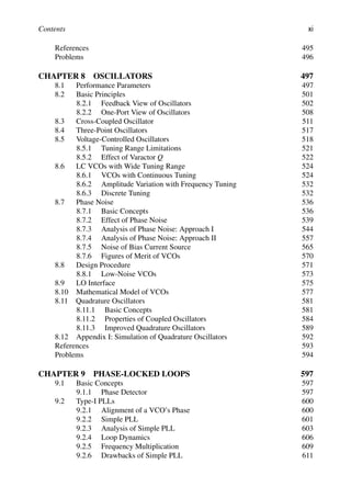
![Sec. 2.1. General Considerations 9
Example 2.2 (Continued)
Solution:
Since the amplifier output voltage swing is of interest, we first convert the received signal
level to voltage. From the previous example, we note that 2100 dBm is 100 dB below
632 mVpp. Also, 100 dB for voltage quantities is equivalent to 105. Thus, 2100 dBm is
equivalent to 6.32 μVpp. This input level is amplified by 15 dB (≈ 5.62), resulting in an
output swing of 35.5 μVpp.
The reader may wonder why the output voltage of the amplifier is of interest in the
above example. This may occur if the circuit following the amplifier does not present a
50- input impedance, and hence the power gain and voltage gain are not equal in dB. In
fact, the next stage may exhibit a purely capacitive input impedance, thereby requiring no
signal “power.” This situation is more familiar in analog circuits wherein one stage drives
the gate of the transistor in the next stage. As explained in Chapter 5, in most integrated
RF systems, we prefer voltage quantities to power quantities so as to avoid confusion if the
input and output impedances of cascade stages are unequal or contain negligible real parts.
The reader may also wonder why we were able to assume 0 dBm is equivalent to
632 mVpp in the above example even though the signal is not a pure sinusoid. After all, only
for a sinusoid can we assume that the rms value is equal to the peak-to-peak value divided
by 2
√
2. Fortunately, for a narrowband 0-dBm signal, it is still possible to approximate the
(average) peak-to-peak swing as 632 mV.
Although dBm is a unit of power, we sometimes use it at interfaces that do not neces-
sarily entail power transfer. For example, consider the case shown in Fig. 2.1(a), where the
LNA drives a purely-capacitive load with a 632-mVpp swing, delivering no average power.
We mentally attach an ideal voltage buffer to node X and drive a 50- load [Fig. 2.1(b)].
We then say that the signal at node X has a level of 0 dBm, tacitly meaning that if this
signal were applied to a 50- load, then it would deliver 1 mW.
M 1
LNA
in
C
M 1
LNA
X
X
50
Av =1
Ω
632 mV
632 mV
(a) (b)
632 mV
Figure 2.1 (a) LNA driving a capacitive impedance, (b) use of fictitious buffer to visualize the signal
level in dBm.
2.1.2 Time Variance
A system is linear if its output can be expressed as a linear combination (superposition) of
responses to individual inputs. More specifically, if the outputs in response to inputs x1(t)](https://image.slidesharecdn.com/rfmicroelectronicsrazavi-230814101614-71259b59/85/RF-MICROELECTRONICS_Razavi-pdf-34-320.jpg)
![10 Chap. 2. Basic Concepts in RF Design
in1
in2 R1
out
in1
in2 R1
out
in1
in2 R1
out
(a) (b) (c)
v
v
v
v
v
v
v
v
v
Figure 2.2 (a) Simple switching circuit, (b) system with Vin1 as the input, (c) system with Vin2 as the
input.
and x2(t) can be respectively expressed as
y1(t) 5 f[x1(t)] (2.9)
y2(t) 5 f[x2(t)], (2.10)
then,
ay1(t) 1 by2(t) 5 f[ax1(t) 1 bx2(t)], (2.11)
for arbitrary values of a and b. Any system that does not satisfy this condition is nonlinear.
Note that, according to this definition, nonzero initial conditions or dc offsets also make a
system nonlinear, but we often relax the rule to accommodate these two effects.
Another attribute of systems that may be confused with nonlinearity is time variance.
A system is time-invariant if a time shift in its input results in the same time shift in its
output. That is, if y(t) 5 f[x(t)], then y(t 2 τ) 5 f[x(t 2 τ)] for arbitrary τ.
As an example of an RF circuit in which time variance plays a critical role and must
not be confused with nonlinearity, let us consider the simple switching circuit shown in
Fig. 2.2(a). The control terminal of the switch is driven by vin1(t) 5 A1 cos ω1t and the input
terminal by vin2(t) 5 A2 cos ω2t. We assume the switch is on if vin1 0 and off otherwise.
Is this system nonlinear or time-variant? If, as depicted in Fig. 2.2(b), the input of interest
is vin1 (while vin2 is part of the system and still equal to A2 cos ω2t), then the system is
nonlinear because the control is only sensitive to the polarity of vin1 and independent of
its amplitude. This system is also time-variant because the output depends on vin2. For
example, if vin1 is constant and positive, then vout(t) 5 vin2(t), and if vin1 is constant and
negative, then vout(t) 5 0 (why?).
Now consider the case shown in Fig. 2.2(c), where the input of interest is vin2
(while vin1 remains part of the system and still equal to A1 cos ω1t). This system is lin-
ear with respect to vin2. For example, doubling the amplitude of vin2 directly doubles that
of vout. The system is also time-variant due to the effect of vin1.
Example 2.3
Plot the output waveform of the circuit in Fig. 2.2(a) if vin1 5 A1 cos ω1t and vin2 5
A2 cos(1.25ω1t).](https://image.slidesharecdn.com/rfmicroelectronicsrazavi-230814101614-71259b59/85/RF-MICROELECTRONICS_Razavi-pdf-35-320.jpg)
![12 Chap. 2. Basic Concepts in RF Design
t t
v in2
1
)
(t
f
0
in2 )
(
V f
f
0
f1
+
f1
+3
f1
f1
−
−3
f
0
f1
+
f1
+3
f1
f1
−
−3
Figure 2.4 Multiplication in the time domain and corresponding convolution in the frequency
domain.
2.1.3 Nonlinearity
A system is called “memoryless” or “static” if its output does not depend on the past values
of its input (or the past values of the output itself). For a memoryless linear system, the
input/output characteristic is given by
y(t) 5 αx(t), (2.15)
where α is a function of time if the system is time-variant [e.g., Fig. 2.2(c)]. For a
memoryless nonlinear system, the input/output characteristic can be approximated with
a polynomial,
y(t) 5 α0 1 α1x(t) 1 α2x2
(t) 1 α3x3
(t) 1 · · ·, (2.16)
where αj may be functions of time if the system is time-variant. Figure 2.5 shows a
common-source stage as an example of a memoryless nonlinear circuit (at low frequen-
cies). If M1 operates in the saturation region and can be approximated as a square-law
device, then
Vout 5 VDD 2 IDRD (2.17)
5 VDD 2
1
2
μnCox
W
L
(Vin 2 VTH)2
RD. (2.18)
In this idealized case, the circuit displays only second-order nonlinearity.
The system described by Eq. (2.16) has “odd symmetry” if y(t) is an odd function of
x(t), i.e., if the response to 2 x(t) is the negative of that to 1 x(t). This occurs if αj 5 0
for even j. Such a system is sometimes called “balanced,” as exemplified by the differential
M 1
RD
VDD
out
V
in
V
Figure 2.5 Common-source stage.](https://image.slidesharecdn.com/rfmicroelectronicsrazavi-230814101614-71259b59/85/RF-MICROELECTRONICS_Razavi-pdf-37-320.jpg)
![Sec. 2.1. General Considerations 13
RD
V
VDD
RD
M M
1 2
I SS
out
in
V
in
V
Vout
(a) (b)
Figure 2.6 (a) Differential pair and (b) its input/output characteristic.
pair shown in Fig. 2.6(a). Recall from basic analog design that by virtue of symmetry, the
circuit exhibits the characteristic depicted in Fig. 2.6(b) if the differential input varies from
very negative values to very positive values.
Example 2.4
For square-law MOS transistors operating in saturation, the characteristic of Fig. 2.6(b) can
be expressed as [1]
Vout 5 2
1
2
μnCox
W
L
Vin
4ISS
μnCox
W
L
2 V2
inRD. (2.19)
If the differential input is small, approximate the characteristic by a polynomial.
Solution:
Factoring 4ISS/(μnCoxW/L) out of the square root and assuming
V2
in
4ISS
μnCox
W
L
, (2.20)
we use the approximation
√
1 2 ≈ 1 2 /2 to write
Vout ≈ 2
μnCox
W
L
ISSVin
1 2
μnCox
W
L
8ISS
V2
in
RD (2.21)
≈ 2
μnCox
W
L
ISSRDVin 1
μnCox
W
L
3/2
8
√
ISS
RDV3
in. (2.22)
The first term on the right-hand side represents linear operation, revealing the small-
signal voltage gain of the circuit (2gmRD). Due to symmetry, even-order nonlinear
terms are absent. Interestingly, square-law devices yield a third-order characteristic in this
case. We return to this point in Chapter 5.](https://image.slidesharecdn.com/rfmicroelectronicsrazavi-230814101614-71259b59/85/RF-MICROELECTRONICS_Razavi-pdf-38-320.jpg)

![Sec. 2.2. Effects of Nonlinearity 17
that the gain experienced by A cos ωt is equal to α1 13α3A2/4 and hence varies appreciably
as A becomes larger.4
We must then ask, do α1 and α3 have the same sign or opposite
signs? Returning to the third-order polynomial in Eq. (2.25), we note that if α1α3 0,
then α1x 1 α3x3 overwhelms α2x2 for large x regardless of the sign of α2, yielding an
“expansive” characteristic [Fig. 2.9(a)]. For example, an ideal bipolar transistor operating
in the forward active region produces a collector current in proportion to exp(VBE/VT),
exhibiting expansive behavior. On the other hand, if α1α3 0, the term α3x3 “bends”
the characteristic for sufficiently large x [Fig. 2.9(b)], leading to “compressive” behavior,
i.e., a decreasing gain as the input amplitude increases. For example, the differential pair
of Fig. 2.6(a) suffers from compression as the second term in (2.22) becomes comparable
with the first. Since most RF circuits of interest are compressive, we hereafter focus on
this type.
x
y
x
1
α
dominant x
dominant
α3
3
x
y
x
1
α
dominant
x
dominant
α3
3
1
α α3 0
1
α α3 0
(a) (b)
Figure 2.9 (a) Expansive and (b) compressive characteristics.
With α1α3 0, the gain experienced by A cos ωt in Eq. (2.28) falls as A rises. We quan-
tify this effect by the “1-dB compression point,” defined as the input signal level that causes
the gain to drop by 1 dB. If plotted on a log-log scale as a function of the input level, the
output level, Aout, falls below its ideal value by 1 dB at the 1-dB compression point, Ain,1dB
(Fig. 2.10). Note that (a) Ain and Aout are voltage quantities here, but compression can also
be expressed in terms of power quantities; (b) 1-dB compression may also be specified in
terms of the output level at which it occurs, Aout,1dB. The input and output compression
points typically prove relevant in the receive path and the transmit path, respectively.
1 dB
20log in
out
A
A
20log
A in,1dB
Figure 2.10 Definition of 1-dB compression point.
4. This effect is akin to the fact that nonlinearity can also be viewed as variation of the slope of the input/output
characteristic with the input level.](https://image.slidesharecdn.com/rfmicroelectronicsrazavi-230814101614-71259b59/85/RF-MICROELECTRONICS_Razavi-pdf-42-320.jpg)
![18 Chap. 2. Basic Concepts in RF Design
To calculate the input 1-dB compression point, we equate the compressed gain, α1 1
(3α3/4)A2
in,1dB, to 1 dB less than the ideal gain, α1:
20 log α1 1
3
4
α3A2
in,1dB 5 20 log |α1| 2 1 dB. (2.33)
It follows that
Ain,1dB 5
0.145
α1
α3
. (2.34)
Note that Eq. (2.34) gives the peak value (rather than the peak-to-peak value) of the input.
Also denoted by P1dB, the 1-dB compression point is typically in the range of 220 to
225 dBm (63.2 to 35.6 mVpp in 50- system) at the input of RF receivers. We use the
notations A1dB and P1dB interchangeably in this book. Whether they refer to the input or
the output will be clear from the context or specified explicitly. While gain compression by
1 dB seems arbitrary, the 1-dB compression point represents a 10% reduction in the gain
and is widely used to characterize RF circuits and systems.
Why does compression matter? After all, it appears that if a signal is so large as to
reduce the gain of a receiver, then it must lie well above the receiver noise and be easily
detectable. In fact, for some modulation schemes, this statement holds and compression of
the receiver would seem benign. For example, as illustrated in Fig. 2.11(a), a frequency-
modulated signal carries no information in its amplitude and hence tolerates compression
(i.e., amplitude limiting). On the other hand, modulation schemes that contain information
in the amplitude are distorted by compression [Fig. 2.11(b)]. This issue manifests itself in
both receivers and transmitters.
Another adverse effect arising from compression occurs if a large interferer accom-
panies the received signal [Fig. 2.12(a)]. In the time domain, the small desired signal is
superimposed on the large interferer. Consequently, the receiver gain is reduced by the
large excursions produced by the interferer even though the desired signal itself is small
(a)
(b)
Frequency Modulation
Amplitude Modulation
Figure 2.11 Effect of compressive nonlinearity on (a) FM and (b) AM waveforms.](https://image.slidesharecdn.com/rfmicroelectronicsrazavi-230814101614-71259b59/85/RF-MICROELECTRONICS_Razavi-pdf-43-320.jpg)
![Sec. 2.2. Effects of Nonlinearity 19
f
Desired
Interferer
Signal
t
Desired Signal + Interferer
(a) (b)
Gain Reduction
Figure 2.12 (a) Interferer accompanying signal, (b) effect in time domain.
[Fig. 2.12(b)]. Called “desensitization,” this phenomenon lowers the signal-to-noise ratio
(SNR) at the receiver output and proves critical even if the signal contains no amplitude
information.
To quantify desensitization, let us assume x(t) 5 A1 cos ω1t 1 A2 cos ω2t, where the
first and second terms represent the desired component and the interferer, respectively. With
the third-order characteristic of Eq. (2.25), the output appears as
y(t) 5
α1 1
3
4
α3A2
1 1
3
2
α3A2
2
A1 cos ω1t 1 · · · . (2.35)
Note that α2 is absent in compression. For A1 A2, this reduces to
y(t) 5
α1 1
3
2
α3A2
2
A1 cos ω1t 1 · · · . (2.36)
Thus, the gain experienced by the desired signal is equal to α1 1 3α3A2
2/2, a decreasing
function of A2 if α1α3 0. In fact, for sufficiently large A2, the gain drops to zero, and we
say the signal is “blocked.” In RF design, the term “blocking signal” or “blocker” refers to
interferers that desensitize a circuit even if they do not reduce the gain to zero. Some RF
receivers must be able to withstand blockers that are 60 to 70 dB greater than the desired
signal.
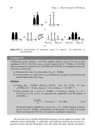
Example 2.7
A 900-MHz GSM transmitter delivers a power of 1 W to the antenna. By how much must
the second harmonic of the signal be suppressed (filtered) so that it does not desensitize a
1.8-GHz receiver having P1dB 5 225 dBm? Assume the receiver is 1 m away (Fig. 2.13)
and the 1.8-GHz signal is attenuated by 10 dB as it propagates across this distance.
(Continues)](https://image.slidesharecdn.com/rfmicroelectronicsrazavi-230814101614-71259b59/85/RF-MICROELECTRONICS_Razavi-pdf-44-320.jpg)
![Sec. 2.2. Effects of Nonlinearity 21
Example 2.8
Suppose an interferer contains phase modulation but not amplitude modulation. Does cross
modulation occur in this case?
Solution:
Expressing the input as x(t) 5 A1 cos ω1t 1 A2 cos(ω2t 1 φ), where the second term rep-
resents the interferer (A2 is constant but φ varies with time), we use the third-order
polynomial in Eq. (2.25) to write
y(t) 5 α1[A1 cos ω1t 1 A2 cos(ω2t 1 φ)] 1 α2[A1 cos ω1t 1 A2 cos(ω2t 1 φ)]2
1 α3[A1 cos ω1t 1 A2 cos(ω2t 1 φ)]3
. (2.38)
We now note that (1) the second-order term yields components at ω1 ± ω2 but not at ω1;
(2) the third-order term expansion gives 3α3A1 cos ω1tA2
2 cos2(ω2t 1 φ), which, according
to cos2 x 5 (1 1 cos 2x)/2, results in a component at ω1. Thus,
y(t) 5
α1 1
3
2
α3A2
2
A1 cos ω1t 1 · · · . (2.39)
Interestingly, the desired signal at ω1 does not experience cross modulation. That is,
phase-modulated interferers do not cause cross modulation in memoryless (static) nonlinear
systems. Dynamic nonlinear systems, on the other hand, may not follow this rule.
Cross modulation commonly arises in amplifiers that must simultaneously process
many independent signal channels. Examples include cable television transmitters and
systems employing “orthogonal frequency division multiplexing” (OFDM). We examine
OFDM in Chapter 3.
2.2.4 Intermodulation
Our study of nonlinearity has thus far considered the case of a single signal (for harmonic
distortion) or a signal accompanied by one large interferer (for desensitization). Another
scenario of interest in RF design occurs if two interferers accompany the desired signal.
Such a scenario represents realistic situations and reveals nonlinear effects that may not
manifest themselves in a harmonic distortion or desensitization test.
If two interferers at ω1 and ω2 are applied to a nonlinear system, the output generally
exhibits components that are not harmonics of these frequencies. Called “intermodulation”
(IM), this phenomenon arises from “mixing” (multiplication) of the two components as
their sum is raised to a power greater than unity. To understand how Eq. (2.25) leads to
intermodulation, assume x(t) 5 A1 cos ω1t 1 A2 cos ω2t. Thus,
y(t) 5 α1(A1 cos ω1t 1 A2 cos ω2t) 1 α2(A1 cos ω1t 1 A2 cos ω2t)2
1 α3(A1 cos ω1t 1 A2 cos ω2t)3
. (2.40)](https://image.slidesharecdn.com/rfmicroelectronicsrazavi-230814101614-71259b59/85/RF-MICROELECTRONICS_Razavi-pdf-46-320.jpg)
![Sec. 2.2. Effects of Nonlinearity 23
Example 2.9 (Continued)
At the same time, Users 2 and 3 transmit at 2.420 GHz and 2.430 GHz, respectively. Explain
what happens.
TX1
TX
TX2
3
RX 4
f (GHz)
2.42
2.41 2.43
User 2
User 3
User 1
User 4
Figure 2.17 Bluetooth RX in the presence of several transmitters.
Solution:
Since the frequencies transmitted by Users 1, 2, and 3 happen to be equally spaced, the
intermodulation in the LNA of RX4 corrupts the desired signal at 2.410 GHz.
The reader may raise several questions at this point: (1) In our analysis of intermod-
ulation, we represented the interferers with pure (unmodulated) sinusoids (called “tones”)
whereas in Figs. 2.16 and 2.17, the interferers are modulated. Are these consistent? (2) Can
gain compression and desensitization (P1dB) also model intermodulation, or do we need
other measures of nonlinearity? (3) Why can we not simply remove the interferers by fil-
ters so that the receiver does not experience intermodulation? We answer the first two here
and address the third in Chapter 4.
For narrowband signals, it is sometimes helpful to “condense” their energy into an
impulse, i.e., represent them with a tone of equal power [Fig. 2.18(a)]. This approxima-
tion must be made judiciously: if applied to study gain compression, it yields reasonably
accurate results; on the other hand, if applied to the case of cross modulation, it fails. In
intermodulation analyses, we proceed as follows: (a) approximate the interferers with tones,
(b) calculate the level of intermodulation products at the output, and (c) mentally convert
the intermodulation tones back to modulated components so as to see the corruption.5
This
thought process is illustrated in Fig. 2.18(b).
We now deal with the second question: if the gain is not compressed, then can we say
that intermodulation is negligible? The answer is no; the following example illustrates this
point.
5. Since a tone contains no randomness, it generally does not corrupt a signal. But a tone appearing in the
spectrum of a signal may make the detection difficult.](https://image.slidesharecdn.com/rfmicroelectronicsrazavi-230814101614-71259b59/85/RF-MICROELECTRONICS_Razavi-pdf-48-320.jpg)
![Sec. 2.2. Effects of Nonlinearity 25
1
ω ω2 ω
−ω
2ω2 1
−ω
2ω1 2
System
Frequency Response
(a)
1
ω ω
2 1
ω
(b)
Figure 2.19 (a) Two-tone and (b) harmonic tests in a narrowband system.
meaningful view of the nonlinear behavior of the system. Depicted in Fig. 2.19(a), this
attribute stands in contrast to harmonic distortion tests, where higher harmonics lie so far
away in frequency that they are heavily filtered, making the system appear quite linear
[Fig. 2.19(b)].
Third Intercept Point Our thoughts thus far indicate the need for a measure of inter-
modulation. A common method of IM characterization is the “two-tone” test, whereby two
pure sinusoids of equal amplitudes are applied to the input. The amplitude of the output IM
products is then normalized to that of the fundamentals at the output. Denoting the peak
amplitude of each tone by A, we can write the result as
Relative IM 5 20 log
3
4
α3
α1
A2
dBc, (2.45)
where the unit dBc denotes decibels with respect to the “carrier” to emphasize the normal-
ization. Note that, if the amplitude of each input tone increases by 6 dB (a factor of two), the
amplitude of the IM products (∝ A3) rises by 18 dB and hence the relative IM by 12 dB.6
The principal difficulty in specifying the relative IM for a circuit is that it is meaningful
only if the value of A is given. From a practical point of view, we prefer a single measure
that captures the intermodulation behavior of the circuit with no need to know the input
level at which the two-tone test is carried out. Fortunately, such a measure exists and is
called the “third intercept point” (IP3).
The concept of IP3 originates from our earlier observation that, if the amplitude of
each tone rises, that of the output IM products increases more sharply (∝ A3). Thus, if
we continue to raise A, the amplitude of the IM products eventually becomes equal to that
6. It is assumed that no compression occurs so that the output fundamental tones also rise by 6 dB.](https://image.slidesharecdn.com/rfmicroelectronicsrazavi-230814101614-71259b59/85/RF-MICROELECTRONICS_Razavi-pdf-50-320.jpg)
![26 Chap. 2. Basic Concepts in RF Design
A
A
α1
log( )
3
4
3
A
α3
log( )
20
20
AIIP3
AOIP3
in
(log scale)
Output
Amplitude
Figure 2.20 Definition of IP3 (for voltage quantities).
of the fundamental tones at the output. As illustrated in Fig. 2.20 on a log-log scale, the
input level at which this occurs is called the “input third intercept point” (IIP3). Similarly,
the corresponding output is represented by OIP3. In subsequent derivations, we denote the
input amplitude as AIIP3.
To determine the IIP3, we simply equate the fundamental and IM amplitudes:
|α1AIIP3| 5
3
4
α3A3
IIP3 , (2.46)
obtaining
AIIP3 5
4
3
α1
α3
. (2.47)
Interestingly,
AIIP3
A1dB
5
4
0.435
(2.48)
≈ 9.6 dB. (2.49)
This ratio proves helpful as a sanity check in simulations and measurements.7
We some-
times write IP3 rather than IIP3 if it is clear from the context that the input is of
interest.
Upon further consideration, the reader may question the consistency of the above
derivations. If the IP3 is 9.6 dB higher than P1dB, is the gain not heavily compressed at
Ain 5 AIIP3?! If the gain is compressed, why do we still express the amplitude of the fun-
damentals at the output as α1A? It appears that we must instead write this amplitude as
[α1 1 (9/4)α3A2]A to account for the compression.
In reality, the situation is even more complicated. The value of IP3 given by Eq. (2.47)
may exceed the supply voltage, indicating that higher-order nonlinearities manifest them-
selves as Ain approaches AIIP3 [Fig. 2.21(a)]. In other words, the IP3 is not a directly
measureable quantity.
In order to avoid these quandaries, we measure the IP3 as follows. We begin with a very
low input level so that α1 1 (9/4)α3A2
in ≈ α1 (and, of course, higher order nonlinearities
7. Note that this relationship holds for a third-order system and not necessarily if higher-order terms manifest
themselves.](https://image.slidesharecdn.com/rfmicroelectronicsrazavi-230814101614-71259b59/85/RF-MICROELECTRONICS_Razavi-pdf-51-320.jpg)
![Sec. 2.2. Effects of Nonlinearity 27
AIIP3
AOIP3
Fundamental
IM3
Fundamental
IM3
Ain
(log scale)
Ain
(log scale)
(a) (b)
Aout
Figure 2.21 (a) Actual behavior of nonlinear circuits, (b) definition of IP3 based on extrapolation.
are also negligible). We increase Ain, plot the amplitudes of the fundamentals and the IM
products on a log-log scale, and extrapolate these plots according to their slopes (one and
three, respectively) to obtain the IP3 [Fig. 2.21(b)]. To ensure that the signal levels remain
well below compression and higher-order terms are negligible, we must observe a 3-dB rise
in the IM products for every 1-dB increase in Ain. On the other hand, if Ain is excessively
small, then the output IM components become comparable with the noise floor of the circuit
(or the noise floor of the simulated spectrum), thus leading to inaccurate results.
Example 2.11
A low-noise amplifier senses a 280-dBm signal at 2.410 GHz and two 220-dBm inter-
ferers at 2.420 GHz and 2.430 GHz. What IIP3 is required if the IM products must remain
20 dB below the signal? For simplicity, assume 50- interfaces at the input and output.
Solution:
Denoting the peak amplitudes of the signal and the interferers by Asig and Aint, respectively,
we can write at the LNA output:
20 log |α1Asig| 2 20 dB 5 20 log
3
4
α3A3
int . (2.50)
It follows that
|α1Asig| 5
30
4
α3A3
int . (2.51)
In a 50- system, the 280-dBm and 220-dBm levels respectively yield Asig 5 31.6 μVp
and Aint 5 31.6 mVp. Thus,
IIP3 5
4
3
α1
α3
(2.52)
5 3.65 Vp (2.53)
5 115.2 dBm. (2.54)
Such an IP3 is extremely difficult to achieve, especially for a complete receiver chain.](https://image.slidesharecdn.com/rfmicroelectronicsrazavi-230814101614-71259b59/85/RF-MICROELECTRONICS_Razavi-pdf-52-320.jpg)
![Sec. 2.2. Effects of Nonlinearity 29
We should remark that second-order nonlinearity also leads to a certain type of inter-
modulation and is characterized by a “second intercept point,” (IP2).8
We elaborate on this
effect in Chapter 4.
2.2.5 Cascaded Nonlinear Stages
Since in RF systems, signals are processed by cascaded stages, it is important to know how
the nonlinearity of each stage is referred to the input of the cascade. The calculation of P1dB
for a cascade is outlined in Problem 2.1. Here, we determine the IP3 of a cascade. For the
sake of brevity, we hereafter denote the input IP3 by AIP3 unless otherwise noted.
Consider two nonlinear stages in cascade (Fig. 2.23). If the input/output characteristics
of the two stages are expressed, respectively, as
y1(t) 5 α1x(t) 1 α2x2
(t) 1 α3x3
(t) (2.57)
y2(t) 5 β1y1(t) 1 β2y2
1(t) 1 β3y3
1(t), (2.58)
then
y2(t) 5 β1[α1x(t) 1 α2x2
(t) 1 α3x3
(t)] 1 β2[α1x(t) 1 α2x2
(t) 1 α3x3
(t)]2
1 β3[α1x(t) 1 α2x2
(t) 1 α3x3
(t)]3
. (2.59)
Considering only the first- and third-order terms, we have
y2(t) 5 α1β1x(t) 1 (α3β1 1 2α1α2β2 1 α3
1β3)x3
(t) 1 · · · . (2.60)
Thus, from Eq. (2.47),
AIP3 5
4
3
α1β1
α3β1 1 2α1α2β2 1 α3
1β3
. (2.61)
IIP IIP
3, 3
1 ,2
( )
t
x ( )
t
y
1
( )
t
y
2
Figure 2.23 Cascaded nonlinear stages.
Example 2.12
Two differential pairs are cascaded. Is it possible to select the denominator of Eq. (2.61)
such that IP3 goes to infinity?
(Continues)
8. As seen in the next section, second-order nonlinearity also affects the IP3 in cascaded systems.](https://image.slidesharecdn.com/rfmicroelectronicsrazavi-230814101614-71259b59/85/RF-MICROELECTRONICS_Razavi-pdf-54-320.jpg)
![30 Chap. 2. Basic Concepts in RF Design
Example 2.12 (Continued)
Solution:
With no asymmetries in the cascade, α2 5 β2 5 0. Thus, we seek the condition α3β1 1
α3
1β3 5 0, or equivalently,
α3
α1
5 2
β3
β1
· α2
1. (2.62)
Since both stages are compressive, α3/α1 0 and β3/β1 0. It is therefore impossible to
achieve an arbitrarily high IP3.
Equation (2.61) leads to more intuitive results if its two sides are squared and inverted:
1
A2
IP3
5
3
4
α3β1 1 2α1α2β2 1 α3
1β3
α1β1
(2.63)
5
3
4
α3
α1
1
2α2β2
β1
1
α2
1β3
β1
(2.64)
5
1
A2
IP3,1
1
3α2β2
2β1
1
α2
1
A2
IP3,2
, (2.65)
where AIP3,1 and AIP3,2 represent the input IP3’s of the first and second stages, respectively.
Note that AIP3, AIP3,1, and AIP3,2 are voltage quantities.
The key observation in Eq. (2.65) is that to “refer” the IP3 of the second stage to the
input of the cascade, we must divide it by α1. Thus, the higher the gain of the first stage,
the more nonlinearity is contributed by the second stage.
IM Spectra in a Cascade To gain more insight into the above results, let us assume
x(t) 5 A cos ω1t 1 A cos ω2t and identify the IM products in a cascade. With the aid of
Fig. 2.24, we make the following observations:9
1. The input tones are amplified by a factor of approximately α1 in the first stage and
β1 in the second. Thus, the output fundamentals are given by α1β1A(cos ω1t 1
cos ω2t).
2. The IM products generated by the first stage, namely, (3α3/4)A3[cos(2ω1 2 ω2)t 1
cos(2ω2 2 ω1)t], are amplified by a factor of β1 when they appear at the output of
the second stage.
3. Sensing α1A(cos ω1t 1 cos ω2t) at its input, the second stage produces its own IM
components: (3β3/4)(α1A)3 cos(2ω1 2 ω2)t 1 (3β3/4)(α1A)3 cos(2ω2 2 ω1)t.
9. The spectrum of A cos ωt consists of two impulses, each with a weight of A/2. We drop the factor of 1/2 in
the figures for simplicity.](https://image.slidesharecdn.com/rfmicroelectronicsrazavi-230814101614-71259b59/85/RF-MICROELECTRONICS_Razavi-pdf-55-320.jpg)
![Sec. 2.2. Effects of Nonlinearity 31
A
( )
ω
ω1 2
ω
2
ω
1
2 ω2 1
ω
2
IIP IIP
3, 3
1 ,2
ω ω
A
α1
2
1
ω ω
A
α1 1
β
ω
2
1
ω
3
4
3
A
α3
ω1 2
ω
ω
2 ω2 1
ω
2
3
4
3
A
α3 1
β
ω1 2
ω
ω
2 ω2 1
ω
2
3
4
3
A
α
β3 1
A
α1
2
1
ω ω ω
ω ω
A
α2
2
2 1 ω1 2
ω
ω
2 ω2 1
ω
2
3
A
α
α1 2 2
β
A
α1
2
1
ω ω ω
A
α2
2
1
2 2
2
ω ω
1
2
ω1 2
ω
ω
2 ω2 1
ω
2
3
A
α
α1 2 2
β
ω ω
1
2
( )
t
x ( )
t
y
1
( )
t
y
2
Figure 2.24 Spectra in a cascade of nonlinear stages.
4. The second-order nonlinearity in y1(t) generates components at ω1 2 ω2, 2ω1, and
2ω2. Upon experiencing a similar nonlinearity in the second stage, these compo-
nents are mixed with those at ω1 and ω2 and translated to 2ω1 2 ω2 and 2ω2 2 ω1.
Specifically, as shown in Fig. 2.24, y2(t) contains terms such as 2β2[α1A cos ω1t 3
α2A2 cos(ω1 2 ω2)t] and 2β2(α1A cos ω1t 3 0.5α2A2 cos 2ω2t). The resulting IM
products can be expressed as (3α1α2β2A3/2)[cos(2ω1 2 ω2)t 1 cos(2ω2 2 ω1)t].
Interestingly, the cascade of two second-order nonlinearities can produce third-
order IM products.
Adding the amplitudes of the IM products, we have
y2(t) 5 α1β1A(cos ω1t 1 cos ω2t)
1
3α3β1
4
1
3α3
1β3
4
1
3α1α2β2
2
A3
[cos(ω1 2 2ω2)t
1 cos(2ω2 2 ω1)t] 1 · · · , (2.66)
obtaining the same IP3 as above. This result assumes zero phase shift for all components.
Why did we add the amplitudes of the IM3 products in Eq. (2.66) without regard for
their phases? Is it possible that phase shifts in the first and second stages allow partial](https://image.slidesharecdn.com/rfmicroelectronicsrazavi-230814101614-71259b59/85/RF-MICROELECTRONICS_Razavi-pdf-56-320.jpg)
![Sec. 2.2. Effects of Nonlinearity 33
IIP IIP
3,1 3,2
1
ω ω2 ω
−ω
2ω2 1
−ω
2ω1 2
1
ω ω2 ω
Δ1
1
ω ω2 ω
−ω
2ω2 1
−ω
2ω1 2
Δ2
Figure 2.25 Growth of IM components along the cascade.
2.2.6 AM/PM Conversion
In some RF circuits, e.g., power amplifiers, amplitude modulation (AM) may be converted
to phase modulation (PM), thus producing undesirable effects. In this section, we study this
phenomenon.
AM/PM conversion (APC) can be viewed as the dependence of the phase shift upon
the signal amplitude. That is, for an input Vin(t) 5 V1 cos ω1t, the fundamental output
component is given by
Vout(t) 5 V2 cos[ω1t 1 φ(V1)], (2.71)
where φ(V1) denotes the amplitude-dependent phase shift. This, of course, does not occur
in a linear time-invariant system. For example, the phase shift experienced by a sinusoid
of frequency ω1 through a first-order low-pass RC section is given by 2 tan21(RCω1)
regardless of the amplitude. Moreover, APC does not appear in a memoryless nonlinear
system because the phase shift is zero in this case.
We may therefore surmise that AM/PM conversion arises if a system is both dynamic
and nonlinear. For example, if the capacitor in a first-order low-pass RC section is nonlin-
ear, then its “average” value may depend on V1, resulting in a phase shift, 2 tan21(RCω1),
that itself varies with V1. To explore this point, let us consider the arrangement shown in
Fig. 2.26 and assume
C1 5 (1 1 αVout)C0. (2.72)
Vin C
R1
Vout
1
Figure 2.26 RC section with nonlinear capacitor.
This capacitor is considered nonlinear because its value depends on its voltage. An
exact calculation of the phase shift is difficult here as it requires that we write
Vin 5 R1C1dVout/dt 1 Vout and hence solve
V1 cos ω1t 5 R1(1 1 αVout)C0
dVout
dt
1 Vout. (2.73)
We therefore make an approximation. Since the value of C1 varies periodically with
time, we can express the output as that of a first-order network but with a time-varying](https://image.slidesharecdn.com/rfmicroelectronicsrazavi-230814101614-71259b59/85/RF-MICROELECTRONICS_Razavi-pdf-58-320.jpg)
![34 Chap. 2. Basic Concepts in RF Design
capacitance, C1(t):
Vout(t) ≈
V1
1 1 R2
1C2
1(t)ω2
1
cos{ω1t 2 tan21
[R1C1(t)ω1]}. (2.74)
If R1C1(t)ω1 1 rad,
Vout(t) ≈ V1 cos[ω1t 2 R1(1 1 αVout)C0ω1]. (2.75)
We also assume that (1 1 αVout)C0 ≈ (1 1 αV1 cos ω1t)C0, obtaining
Vout(t) ≈ V1 cos(ω1t 2 R1C0ω1 2 αR1C0ω1V1 cos ω1t). (2.76)
Does the output fundamental contain an input-dependent phase shift here? No, it does
not! The reader can show that the third term inside the parentheses produces only higher
harmonics. Thus, the phase shift of the fundamental is equal to 2R1C0ω1 and hence
constant.
The above example entails no AM/PM conversion because of the first-order depen-
dence of C1 upon Vout. As illustrated in Fig. 2.27, the average value of C1 is equal to
C0 regardless of the output amplitude. In general, since C1 varies periodically, it can be
expressed as a Fourier series with a “dc” term representing its average value:
C1(t) 5 Cavg 1
∞
n51
an cos(nω1t) 1
∞
n51
bn sin(nω1t). (2.77)
Thus, if Cavg is a function of the amplitude, then the phase shift of the fundamental com-
ponent in the output voltage becomes input-dependent. The following example illustrates
this point.
t
C1
C0
t
Vout
C1
Figure 2.27 Time variation of capacitor with first-order voltage dependence for small and large
swings.](https://image.slidesharecdn.com/rfmicroelectronicsrazavi-230814101614-71259b59/85/RF-MICROELECTRONICS_Razavi-pdf-59-320.jpg)
![Sec. 2.3. Noise 35
Example 2.14
Suppose C1 in Fig. 2.26 is expressed as C1 5 C0(1 1 α1Vout 1 α2V2
out). Study the AM/PM
conversion in this case if Vin(t) 5 V1 cos ω1t.
Solution:
Figure 2.28 plots C1(t) for small and large input swings, revealing that Cavg indeed depends
on the amplitude. We rewrite Eq. (2.75) as
t
C1
C0
t
Vout
C1
Cavg1
Cavg2
Figure 2.28 Time variation of capacitor with second-order voltage dependence for small and large
swings.
Vout(t) ≈ V1 cos[ω1t 2 R1C0ω1(1 1 α1V1 cos ω1t 1 α2V2
1 cos2
ω1t)] (2.78)
≈ V1 cos(ω1t 2 R1C0ω1 2
α2R1C0ω1V2
1
2
2 · · · ). (2.79)
The phase shift of the fundamental now contains an input-dependent term,
2(α2R1C0ω1V2
1 )/2. Figure 2.28 also suggests that AM/PM conversion does not occur if
the capacitor voltage dependence is odd-symmetric.
What is the effect of APC? In the presence of APC, amplitude modulation (or amplitude
noise) corrupts the phase of the signal. For example, if Vin(t) 5 V1(11m cos ωmt) cos ω1t,
then Eq. (2.79) yields a phase corruption equal to 2α2R1C0ω1(2mV1 cos ωmt 1
m2V2
1 cos2 ωmt)/2. We will encounter examples of APC in Chapters 8 and 12.
2.3 NOISE
The performance of RF systems is limited by noise. Without noise, an RF receiver would
be able to detect arbitrarily small inputs, allowing communication across arbitrarily long](https://image.slidesharecdn.com/rfmicroelectronicsrazavi-230814101614-71259b59/85/RF-MICROELECTRONICS_Razavi-pdf-60-320.jpg)
![36 Chap. 2. Basic Concepts in RF Design
distances. In this section, we review basic properties of noise and methods of calculat-
ing noise in circuits. For a more complete study of noise in analog circuits, the reader is
referred to [1].
2.3.1 Noise as a Random Process
The trouble with noise is that it is random. Engineers who are used to dealing with well-
defined, deterministic, “hard” facts often find the concept of randomness difficult to grasp,
especially if it must be incorporated mathematically. To overcome this fear of randomness,
we approach the problem from an intuitive angle.
By “noise is random,” we mean the instantaneous value of noise cannot be predicted.
For example, consider a resistor tied to a battery and carrying a current [Fig. 2.29(a)].
Due to the ambient temperature, each electron carrying the current experiences thermal
agitation, thus following a somewhat random path while, on the average, moving toward
the positive terminal of the battery. As a result, the average current remains equal to VB/R
but the instantaneous current displays random values.10
VB
t
VB
R
R
VB
t
VB
R
R
(a) (b)
Figure 2.29 (a) Noise generated in a resistor, (b) effect of higher temperature.
Since noise cannot be characterized in terms of instantaneous voltages or currents, we
seek other attributes of noise that are predictable. For example, we know that a higher ambi-
ent temperature leads to greater thermal agitation of electrons and hence larger fluctuations
in the current [Fig. 2.29(b)]. How do we express the concept of larger random swings for
a current or voltage quantity? This property is revealed by the average power of the noise,
defined, in analogy with periodic signals, as
Pn 5 lim
T→∞
1
T
T
0
n2
(t)dt, (2.80)
where n(t) represents the noise waveform. Illustrated in Fig. 2.30, this definition simply
means that we compute the area under n2(t) for a long time, T, and normalize the result
to T, thus obtaining the average power. For example, the two scenarios depicted in Fig. 2.29
yield different average powers.
10. As explained later, this is true even with a zero average current.](https://image.slidesharecdn.com/rfmicroelectronicsrazavi-230814101614-71259b59/85/RF-MICROELECTRONICS_Razavi-pdf-61-320.jpg)

![40 Chap. 2. Basic Concepts in RF Design
example, if white noise is applied to a low-pass filter, how do we determine the PSD at
the output? As shown in Fig. 2.33, we intuitively expect that the output PSD assumes the
shape of the filter’s frequency response. In fact, if x(t) is applied to a linear, time-invariant
system with a transfer function H(s), then the output spectrum is
Sy( f) 5 Sx( f)|H( f)|2
, (2.86)
where H( f) 5 H(s 5 j2πf) [2]. We note that |H( f)| is squared because Sx( f) is a (voltage
or current) squared quantity.
f
LPF
f
Figure 2.33 Effect of low-pass filter on white noise.
2.3.4 Device Noise
In order to analyze the noise performance of circuits, we wish to model the noise of their
constituent elements by familiar components such as voltage and current sources. Such a
representation allows the use of standard circuit analysis techniques.
Thermal Noise of Resistors As mentioned previously, the ambient thermal energy leads
to random agitation of charge carriers in resistors and hence noise. The noise can be
modeled by a series voltage source with a PSD of V2
n 5 4kTR1 [Thevenin equivalent,
Fig. 2.34(a)] or a parallel current source with a PSD of I2
n 5 V2
n /R1 5 4kT/R1 [Norton
equivalent, Fig. 2.34(b)]. The choice of the model sometimes simplifies the analysis.
The polarity of the sources is unimportant (but must be kept the same throughout the
calculations of a given circuit).
R1
4kTR1
R1
4kT
R1
(a) (b)
Figure 2.34 (a) Thevenin and (b) Norton models of resistor thermal noise.
Example 2.16
Sketch the PSD of the noise voltage measured across the parallel RLC tank depicted in
Fig. 2.35(a).](https://image.slidesharecdn.com/rfmicroelectronicsrazavi-230814101614-71259b59/85/RF-MICROELECTRONICS_Razavi-pdf-65-320.jpg)
![Sec. 2.3. Noise 41
Example 2.16 (Continued)
(a) (b)
L1 C1
R1 )
(t 4kT
R1
L1 C1
R1 )
(t
n
f
)
(
S f
V
4kTR1
f0
(c)
V
n
V
Figure 2.35 (a) RLC tank, (b) inclusion of resistor noise, (c) output noise spectrum due to R1.
Solution:
Modeling the noise of R1 by a current source, I2
n1 5 4kT/R1, [Fig. 2.35(b)] and noting that
the transfer function Vn/In1 is, in fact, equal to the impedance of the tank, ZT, we write
from Eq. (2.86)
V2
n 5 I2
n1|ZT|2
. (2.87)
At f0 5 (2π
√
L1C1)21, L1 and C1 resonate, reducing the circuit to only R1. Thus, the output
noise at f0 is simply equal to I2
n1R2
1 5 4kTR1. At lower or higher frequencies, the impedance
of the tank falls and so does the output noise [Fig. 2.35(c)].
If a resistor converts the ambient heat to a noise voltage or current, can we extract
energy from the resistor? In particular, does the arrangement shown in Fig. 2.36 deliver
energy to R2? Interestingly, if R1 and R2 reside at the same temperature, no net energy is
transferred between them because R2 also produces a noise PSD of 4kTR2 (Problem 2.8).
However, suppose R2 is held at T 5 0 K. Then, R1 continues to draw thermal energy from
its environment, converting it to noise and delivering the energy to R2. The average power
transferred to R2 is equal to
PR2 5
V2
out
R2
(2.88)
5 V2
n
R2
R1 1 R2
2
1
R2
(2.89)
5 4kT
R1R2
(R1 1 R2)2
. (2.90)
Vn
2
4kTR1
R
R
=
2
1
Vout
Figure 2.36 Transfer of noise from one resistor to another.](https://image.slidesharecdn.com/rfmicroelectronicsrazavi-230814101614-71259b59/85/RF-MICROELECTRONICS_Razavi-pdf-66-320.jpg)
![42 Chap. 2. Basic Concepts in RF Design
This quantity reaches a maximum if R2 5 R1:
PR2,max 5 kT. (2.91)
Called the “available noise power,” kT is independent of the resistor value and has the
dimension of power per unit bandwidth. The reader can prove that kT 5 2173.8 dBm/Hz
at T 5 300 K.
For a circuit to exhibit a thermal noise density of V2
n 5 4kTR1, it need not contain an
explicit resistor of value R1. After all, Eq. (2.86) suggests that the noise density of a resistor
may be transformed to a higher or lower value by the surrounding circuit. We also note that
if a passive circuit dissipates energy, then it must contain a physical resistance15
and must
therefore produce thermal noise. We loosely say “lossy circuits are noisy.”
A theorem that consolidates the above observations is as follows: If the real part of
the impedance seen between two terminals of a passive (reciprocal) network is equal to
Re{Zout}, then the PSD of the thermal noise seen between these terminals is given by V2
n 5
4kTRe{Zout} (Fig. 2.37) [8]. This general theorem is not limited to lumped circuits. For
example, consider a transmitting antenna that dissipates energy by radiation according to
the equation V2
TX,rms/Rrad, where Rrad is the “radiation resistance” [Fig. 2.38(a)]. As a
receiving element [Fig. 2.38(b)], the antenna generates a thermal noise PSD of16
V2
n,ant 5 4kTRrad. (2.92)
out
Z
4kT
Re{ out
Z
}
out
Z
Figure 2.37 Output noise of a passive (reciprocal) circuit.
VX
Rrad
R
4kTR
rad
rad
(a) (b)
Figure 2.38 (a) Transmitting antenna, (b) receiving antenna producing thermal noise.
15. Recall that ideal inductors and capacitors store energy but do not dissipate it.
16. Strictly speaking, this is not correct because the noise of a receiving antenna is in fact given by the “back-
ground” noise (e.g., cosmic radiation). However, in RF design, the antenna noise is commonly assumed to be
4kTRrad.](https://image.slidesharecdn.com/rfmicroelectronicsrazavi-230814101614-71259b59/85/RF-MICROELECTRONICS_Razavi-pdf-67-320.jpg)
![Sec. 2.3. Noise 43
M 1
4kT γ g m
M 1
4kT γ
g m
(a) (b)
Figure 2.39 Thermal channel noise of a MOSFET modeled as a (a) current source, (b) voltage
source.
Noise in MOSFETs The thermal noise of MOS transistors operating in the saturation
region is approximated by a current source tied between the source and drain terminals
[Fig. 2.39(a)]:
I2
n 5 4kTγ gm, (2.93)
where γ is the “excess noise coefficient” and gm the transconductance.17
The value of γ
is 2/3 for long-channel transistors and may rise to even 2 in short-channel devices [4].
The actual value of γ has other dependencies [5] and is usually obtained by measure-
ments for each generation of CMOS technology. In Problem 2.10, we prove that the noise
can alternatively be modeled by a voltage source V2
n 5 4kTγ/gm in series with the gate
[Fig. 2.39(b)].
Another component of thermal noise arises from the gate resistance of MOSFETs, an
effect that becomes increasingly more important as the gate length is scaled down. Illus-
trated in Fig. 2.40(a) for a device with a width of W and a length of L, this resistance
amounts to
RG 5
W
L
R, (2.94)
where R denotes the sheet resistance (resistance of one square) of the polysilicon gate.
For example, if W 5 1 μm, L 5 45 nm, and R 5 15 , then RG 5 333 . Since RG is dis-
tributed over the width of the transistor [Fig. 2.40(b)], its noise must be calculated carefully.
As proved in [6], the structure can be reduced to a lumped model having an equivalent gate
resistance of RG/3 with a thermal noise PSD of 4kTRG/3 [Fig. 2.40(c)]. In a good design,
this noise must be much less than that of the channel:
4kT
RG
3
4kTγ
gm
. (2.95)
The gate and drain terminals also exhibit physical resistances, which are minimized through
the use of multiple fingers.
At very high frequencies the thermal noise current flowing through the channel couples
to the gate capacitively, thus generating a “gate-induced noise current” [3] (Fig. 2.41). This
17. More accurately, I2
n 5 4kTγ gd0, where gd0 is the drain-source conductance in the triode region (even
though the noise is measured in saturation) [3].](https://image.slidesharecdn.com/rfmicroelectronicsrazavi-230814101614-71259b59/85/RF-MICROELECTRONICS_Razavi-pdf-68-320.jpg)
![44 Chap. 2. Basic Concepts in RF Design
RG1 RG2 RGn
S
D
G
RG1 RG2 RGn
+ + + = RG
R
3
4kTRG
3
G
(c)
(a)
(b)
W
L
W
L
Gate
Drain
Source
Figure 2.40 (a) Gate resistance of a MOSFET, (b) equivalent circuit for noise calculation,
(c) equivalent noise and resistance in lumped model.
I
2
G
I
2
n
Gate Channel
Figure 2.41 Gate-induced noise, I2
G.
effect is not modeled in typical circuit simulators, but its significance has remained unclear.
In this book, we neglect the gate-induced noise current.
MOS devices also suffer from “flicker” or “1/f” noise. Modeled by a voltage source in
series with the gate, this noise exhibits the following PSD:
V2
n 5
K
WLCox
1
f
, (2.96)
where K is a process-dependent constant. In most CMOS technologies, K is lower for
PMOS devices than for NMOS transistors because the former carry charge well below the
silicon-oxide interface and hence suffer less from “surface states” (dangling bonds) [1]. The
1/f dependence means that noise components that vary slowly assume a large amplitude.
The choice of the lowest frequency in the noise integration depends on the time scale of
interest and/or the spectrum of the desired signal [1].](https://image.slidesharecdn.com/rfmicroelectronicsrazavi-230814101614-71259b59/85/RF-MICROELECTRONICS_Razavi-pdf-69-320.jpg)
![Sec. 2.3. Noise 47
Noisy
Circuit Circuit
V 2
I n
2
n
Noiseless
Model A Model B
Figure 2.45 Input-referred noise.
In analog design, the input-referred noise is modeled by a series voltage source and a
parallel current source (Fig. 2.45) [1]. The former is obtained by shorting the input port
of models A and B and equating their output noises (or, equivalently, dividing the output
noise by the voltage gain). Similarly, the latter is computed by leaving the input ports
open and equating the output noises (or, equivalently, dividing the output noise by the
transimpedance gain).
Example 2.18
Calculate the input-referred noise of the common-gate stage depicted in Fig. 2.46(a).
Assume I1 is ideal and neglect the noise of R1.
Vb
VDD
M 1
V
Vin
out
r O
I 1
R
Zin
M 1
r O
R
V
2
n1
I
2
M 1
r O
R
V
2
I
2
(c)
(a) (b)
n2
1
1
1
n
n
Figure 2.46 (a) CG stage, (b) computation of input-referred noise voltage, (c) computation of
input-referred noise current.
Solution:
Shorting the input to ground, we write from Fig. 2.46(b),
V2
n1 5 I2
n · r2
O. (2.103)
Since the voltage gain of the stage is given by 1 1 gmrO, the input-referred noise voltage is
equal to
V2
n,in 5
I2
nr2
O
(1 1 gmrO)2
(2.104)
≈
4kTγ
gm
, (2.105)
(Continues)](https://image.slidesharecdn.com/rfmicroelectronicsrazavi-230814101614-71259b59/85/RF-MICROELECTRONICS_Razavi-pdf-72-320.jpg)
![48 Chap. 2. Basic Concepts in RF Design
Example 2.18 (Continued)
where it is assumed gmrO 1. Leaving the input open as shown in Fig. 2.46(c), the reader
can show that (Problem 2.12)
V2
n2 5 I2
nr2
O. (2.106)
Defined as the output voltage divided by the input current, the transimpedance gain of the
stage is given by gmrOR1 (why?). It follows that
I2
n,in 5
I2
nr2
O
g2
mr2
OR2
1
(2.107)
5
4kTγ
gmR2
1
. (2.108)
From the above example, it may appear that the noise of M1 is “counted” twice. It
can be shown that [1] the two input-referred noise sources are necessary and sufficient, but
often correlated.
Example 2.19
Explain why the output noise of a circuit depends on the output impedance of the preceding
stage.
Solution:
Modeling the noise of the circuit by input-referred sources as shown in Fig. 2.47, we
observe that some of I2
n flows through Z1, generating a noise voltage at the input that
depends on |Z1|. Thus, the output noise, Vn,out, also depends on |Z1|.
Z 1
Z 1
V
2
n
I
2
n
Vn,out Vn,out
Figure 2.47 Noise in a cascade.
The computation and use of input-referred noise sources prove difficult at high fre-
quencies. For example, it is quite challenging to measure the transimpedance gain of an
RF stage. For this reason, RF designers employ the concept of “noise figure” as another
metric of noise performance that more easily lends itself to measurement.
Noise Figure In circuit and system design, we are interested in the signal-to-noise ratio
(SNR), defined as the signal power divided by the noise power. It is therefore helpful to](https://image.slidesharecdn.com/rfmicroelectronicsrazavi-230814101614-71259b59/85/RF-MICROELECTRONICS_Razavi-pdf-73-320.jpg)
![Sec. 2.3. Noise 49
ask, how does the SNR degrade as the signal travels through a given circuit? If the circuit
contains no noise, then the output SNR is equal to the input SNR even if the circuit acts as
an attenuator.18
To quantify how noisy the circuit is, we define its noise figure (NF) as
NF 5
SNRin
SNRout
(2.109)
such that it is equal to 1 for a noiseless stage. Since each quantity in this ratio has a
dimension of power (or voltage squared), we express NF in decibels as
NF|dB 5 10 log
SNRin
SNRout
. (2.110)
Note that most texts call (2.109) the “noise factor” and (2.110) the noise figure. We do not
make this distinction in this book.
Compared to input-referred noise, the definition of NF in (2.109) may appear rather
complicated: it depends on not only the noise of the circuit under consideration but the
SNR provided by the preceding stage. In fact, if the input signal contains no noise, then
SNRin 5 ∞ and NF 5 ∞, even though the circuit may have finite internal noise. For
such a case, NF is not a meaningful parameter and only the input-referred noise can be
specified.
Calculation of the noise figure is generally simpler than Eq. (2.109) may suggest.
For example, suppose a low-noise amplifier senses the signal received by an antenna
[Fig. 2.48(a)]. As predicted by Eq. (2.92), the antenna “radiation resistance,” RS, pro-
duces thermal noise, leading to the model shown in Fig. 2.48(b). Here, V2
n,RS represents the
thermal noise of the antenna, and V2
n the output noise of the LNA. We must compute SNRin
at the LNA input and SNRout at its output.
LNA
out
V
R
Vin
V
2
S
Circuit
Noiseless
Zin
Antenna SNRin
n,RS V
2
n
Vout
SNRout
LNA
A v
(a) (b)
Figure 2.48 (a) Antenna followed by LNA, (b) equivalent circuit.
18. Because the input signal and the input noise are attenuated by the same factor.](https://image.slidesharecdn.com/rfmicroelectronicsrazavi-230814101614-71259b59/85/RF-MICROELECTRONICS_Razavi-pdf-74-320.jpg)
![Sec. 2.3. Noise 51
from Vin to Vout and normalize the result to the noise of RS.” Alternatively, we can say from
(2.115) that “we calculate the output noise due to the amplifier (V2
n ), divide it by the gain,
normalize it to 4kTRS, and add 1 to the result.”
It is important to note that the above derivations are valid even if no actual power is
transferred from the antenna to the LNA or from the LNA to a load. For example, if Zin
in Fig. 2.48(b) goes to infinity, no power is delivered to the LNA, but all of the deriva-
tions remain valid because they are based on voltage (squared) quantities rather than power
quantities. In other words, so long as the derivations incorporate noise and signal volt-
ages, no inconsistency arises in the presence of impedance mismatches or even infinite
input impedances. This is a critical difference in thinking between modern RF design and
traditional microwave design.
Example 2.20
Compute the noise figure of a shunt resistor RP with respect to a source impedance RS
[Fig. 2.49(a)].
Vin
RS
Vout
V 2
(a) (b)
RP RP
RS
n,out
Figure 2.49 (a) Circuit consisting of a single parallel resistor, (b) model for NF calculation.
Solution:
From Fig. 2.49(b), the total output noise voltage is obtained by setting Vin to zero:
V2
n,out 5 4kT(RS||RP). (2.117)
The gain is equal to
A0 5
RP
RP 1 RS
. (2.118)
Thus,
NF 5 4kT(RS||RP)
(RS 1 RP)2
R2
P
1
4kTRS
(2.119)
5 1 1
RS
RP
. (2.120)
The NF is therefore minimized by maximizing RP. Note that if RP 5 RS to provide
impedance matching, then the NF cannot be less than 3 dB. We will return to this critical
point in the context of LNA design in Chapter 5.](https://image.slidesharecdn.com/rfmicroelectronicsrazavi-230814101614-71259b59/85/RF-MICROELECTRONICS_Razavi-pdf-76-320.jpg)
![54 Chap. 2. Basic Concepts in RF Design
Let us now consider the second stage by itself and determine its noise figure with
respect to a source impedance of Rout1 [Fig. 2.51(b)]. Using (2.115) again, we have
NF2 5 1 1
V2
n2
R2
in2
(Rin2 1 Rout1)2
A2
v2
1
4kTRout1
. (2.127)
It follows from (2.126) and (2.127) that
NFtot 5 NF1 1
NF2 2 1
R2
in1
(Rin1 1 RS)2
A2
v1
RS
Rout1
. (2.128)
What does the denominator represent? This quantity is in fact the “available power gain”
of the first stage, defined as the “available power” at its output, Pout,av (the power that it
would deliver to a matched load) divided by the available source power, PS,av (the power
that the source would deliver to a matched load). This can be readily verified by finding the
power that the first stage in Fig. 2.51(a) would deliver to a load equal to Rout1:
Pout,av 5 V2
in
R2
in1
(RS 1 Rin1)2
A2
v1 ·
1
4Rout1
. (2.129)
Similarly, the power that Vin would deliver to a load of RS is given by
PS,av 5
V2
in
4RS
. (2.130)
The ratio of (2.129) and (2.130) is indeed equal to the denominator in (2.128).
With these observations, we write
NFtot 5 NF1 1
NF2 2 1
AP1
, (2.131)
where AP1 denotes the “available power gain” of the first stage. It is important to bear in
mind that NF2 is computed with respect to the output impedance of the first stage. For m
stages,
NFtot 5 1 1 (NF1 2 1) 1
NF2 2 1
AP1
1 · · · 1
NFm 2 1
AP1 · · · AP(m21)
. (2.132)
Called “Friis’ equation” [7], this result suggests that the noise contributed by each stage
decreases as the total gain preceding that stage increases, implying that the first few stages
in a cascade are the most critical. Conversely, if a stage suffers from attenuation (loss),
then the NF of the following circuits is “amplified” when referred to the input of that
stage.](https://image.slidesharecdn.com/rfmicroelectronicsrazavi-230814101614-71259b59/85/RF-MICROELECTRONICS_Razavi-pdf-79-320.jpg)
![58 Chap. 2. Basic Concepts in RF Design
Note that RL is assumed noiseless so that only the noise figure of the lossy circuit can be
determined. The voltage gain from Vin to Vout is found by noting that, in response to Vin, the
circuit produces an output voltage of Vout 5 VThevRL/(RL 1 Rout) [Fig. 2.54(b)]. That is,
A0 5
VThev
Vin
RL
RL 1 Rout
. (2.140)
The NF is equal to (2.139) divided by the square of (2.140) and normalized to 4kTRS:
NF 5 4kTRout
V2
in
V2
Thev
1
4kTRS
(2.141)
5 L. (2.142)
Example 2.24
The receiver shown in Fig. 2.55 incorporates a front-end band-pass filter (BPF) to suppress
some of the interferers that may desensitize the LNA. If the filter has a loss of L and the
LNA a noise figure of NFLNA, calculate the overall noise figure.
LNA
out
V
BPF
Figure 2.55 Cascade of BPF and LNA.
Solution:
Denoting the noise figure of the filter by NFfilt, we write Friis’ equation as
NFtot 5 NFfilt 1
NFLNA 2 1
L21
(2.143)
5 L 1 (NFLNA 2 1)L (2.144)
5 L · NFLNA, (2.145)
where NFLNA is calculated with respect to the output resistance of the filter. For example,
if L 5 1.5 dB and NFLNA 5 2 dB, then NFtot 5 3.5 dB.
2.4 SENSITIVITY AND DYNAMIC RANGE
The performance of RF receivers is characterized by many parameters. We study two,
namely, sensitivity and dynamic range, here and defer the others to Chapter 3.](https://image.slidesharecdn.com/rfmicroelectronicsrazavi-230814101614-71259b59/85/RF-MICROELECTRONICS_Razavi-pdf-83-320.jpg)
![Sec. 2.5. Passive Impedance Transformation 63
networks,” such circuits do not easily lend themselves to integration because their con-
stituent devices, particularly inductors, suffer from loss if built on silicon chips. (We do
use on-chip inductors in many RF building blocks.) Nonetheless, a basic understanding of
impedance transformation is essential.
2.5.1 Quality Factor
In its simplest form, the quality factor, Q, indicates how close to ideal an energy-storing
device is. An ideal capacitor dissipates no energy, exhibiting an infinite Q, but a series
resistance, RS [Fig. 2.57(a)], reduces its Q to
QS 5
1
Cω
RS
, (2.163)
where the numerator denotes the “desired” component and the denominator, the “unde-
sired” component. If the resistive loss in the capacitor is modeled by a parallel resistance
[Fig. 2.57(b)], then we must define the Q as
QP 5
RP
1
Cω
, (2.164)
because an ideal (infinite Q) results only if RP 5 ∞. As depicted in Figs. 2.57(c) and (d),
similar concepts apply to inductors
QS 5
Lω
RS
(2.165)
QP 5
RP
Lω
. (2.166)
While a parallel resistance appears to have no physical meaning, modeling the loss by RP
proves useful in many circuits such as amplifiers and oscillators (Chapters 5 and 8). We
will also introduce other definitions of Q in Chapter 8.
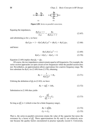
2.5.2 Series-to-Parallel Conversion
Before studying transformation techniques, let us consider the series and parallel RC
sections shown in Fig. 2.58. What choice of values makes the two networks equivalent?
R C
S
RP
C
RS
L RP
L
(c)
(a) (b (
) d)
Figure 2.57 (a) Series RC circuit, (b) equivalent parallel circuit, (c) series RL circuit, (d) equivalent
parallel circuit.](https://image.slidesharecdn.com/rfmicroelectronicsrazavi-230814101614-71259b59/85/RF-MICROELECTRONICS_Razavi-pdf-88-320.jpg)
![Sec. 2.5. Passive Impedance Transformation 65
parallel-to-series conversion reduces the resistance by a factor of Q2
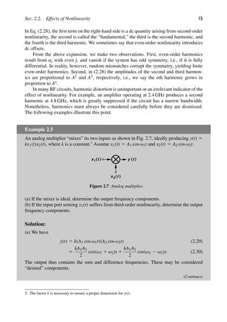
P. This statement applies
to RL sections as well.
2.5.3 Basic Matching Networks
A common situation in RF transmitter design is that a load resistance must be transformed
to a lower value. The circuit shown in Fig. 2.59(a) accomplishes this task. As mentioned
above, the capacitor in parallel with RL converts this resistance to a lower series component
[Fig. 2.59(b)]. The inductance is inserted to cancel the equivalent series capacitance.
L1
C1 R
Zin
L
L1
R
Zin
C1
S
(a) (b)
Figure 2.59 (a) Matching network, (b) equivalent circuit.
Writing Zin from Fig. 2.59(a) and replacing s with jω, we have
Zin( jω) 5
RL(1 2 L1C1ω2) 1 jL1ω
1 1 jRLC1ω
. (2.176)
Thus,
Re{Zin} 5
RL
1 1 R2
LC2
1ω2
(2.177)
5
RL
1 1 Q2
P
, (2.178)
indicating that RL is transformed down by a factor of 1 1 Q2
P. Also, setting the imaginary
part to zero gives
L1 5
R2
LC1
1 1 R2
LC2
1ω2
(2.179)
5
R2
LC1
1 1 Q2
P
. (2.180)
If Q2
P 1, then
Re{Zin} ≈
1
RLC2
1ω2
(2.181)
L1 5
1
C1ω2
. (2.182)
The following example illustrates how the component values are chosen.](https://image.slidesharecdn.com/rfmicroelectronicsrazavi-230814101614-71259b59/85/RF-MICROELECTRONICS_Razavi-pdf-90-320.jpg)
![66 Chap. 2. Basic Concepts in RF Design
Example 2.27
Design the matching network of Fig. 2.59(a) so as to transform RL 5 50 to 25 at a
center frequency of 5 GHz.
Solution:
Assuming Q2
P 1, we have from Eqs. (2.181) and (2.182), C1 5 0.90 pF and L1 5 1.13 nH,
respectively. Unfortunately, however, QP 5 1.41, indicating that Eqs. (2.178) and (2.180)
must be used instead. We thus obtain C1 5 0.637 pF and L1 5 0.796 nH.
In order to transform a resistance to a higher value, the capacitive network shown in
Fig. 2.60(a) can be used. The series-parallel conversion results derived previously pro-
vide insight here. If Q2 1, the parallel combination of C1 and RL can be converted to
a series network [Fig. 2.60(b)], where RS ≈ [RL(C1ω)2]21 and CS ≈ C1. Viewing C2 and
C1 as one capacitor, Ceq, and converting the resulting series section to a parallel circuit
[Fig. 2.60(c)], we have
Rtot 5
1
RS(Ceqω)2
(2.183)
5
1 1
C1
C2
2
RL. (2.184)
That is, the network “boosts” the value of RL by a factor of (1 1 C1/C2)2. Also,
Ceq 5
C1C2
C1 1 C2
. (2.185)
Note that the capacitive component must be cancelled by placing an inductor in parallel
with the input.
C1 R
in
L R
C1
S
(a) (b)
C2
Y
C2
in
Y
R
C
(c)
tot
eq
Figure 2.60 (a) Capacitive matching circuit, (b) simplified circuit with parallel-to-series conver-
sion, (c) simplified circuit with series-to-parallel conversion.
For low Q values, the above derivations incur significant error. We thus compute the
input admittance (1/Yin) and replace s with jω,
Yin 5
jωC2(1 1 jωRLC1)
1 1 RL(C1 1 C2)jω
. (2.186)](https://image.slidesharecdn.com/rfmicroelectronicsrazavi-230814101614-71259b59/85/RF-MICROELECTRONICS_Razavi-pdf-91-320.jpg)
![Sec. 2.5. Passive Impedance Transformation 67
The real part of Yin yields the equivalent resistance seen to ground if we write
Rtot 5
1
Re{Yin}
(2.187)
5
1
RLC2
2ω2
1 RL
1 1
C1
C2
2
. (2.188)
In comparison with Eq. (2.184), this result contains an additional component, (RLC2
2ω2)21.
Example 2.28
Determine how the circuit shown in Fig. 2.61(a) transforms RL.
L1
C1 R
Zin
L
(a) (b)
C1 R
Zin
L1 P
Figure 2.61 (a) Matching network, (b) simplified circuit.
Solution:
We postulate that conversion of the L1–RL branch to a parallel section produces a higher
resistance. If Q2
S 5 (L1ω/RL)2 1, then the equivalent parallel resistance is obtained from
Eq. (2.174) as
RP 5 Q2
SRL (2.189)
5
L2
1ω2
RL
. (2.190)
The parallel equivalent inductance is approximately equal to L1 and is cancelled by C1
[Fig. 2.61(b)].
The intuition gained from our analysis of matching networks leads to the four
“L-section” topologies24
shown in Fig. 2.62. In Fig. 2.62(a), C1 transforms RL to a smaller
series value and L1 cancels C1. Similarly, in Fig. 2.62(b), L1 transforms RL to a smaller
series value while C1 resonates with L1. In Fig. 2.62(c), L1 transforms RL to a larger paral-
lel value and C1 cancels the resulting parallel inductance. A similar observation applies to
Fig. 2.62(d).
How do these networks transform voltages and currents? As an example, consider the
circuit in Fig. 2.62(a). For a sinusoidal input voltage with an rms value of Vin, the power
24. The term “L” is used because the capacitor and the inductor form the letter L in the circuit diagram.](https://image.slidesharecdn.com/rfmicroelectronicsrazavi-230814101614-71259b59/85/RF-MICROELECTRONICS_Razavi-pdf-92-320.jpg)
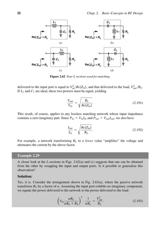
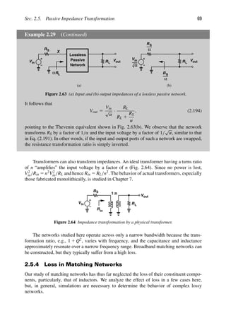
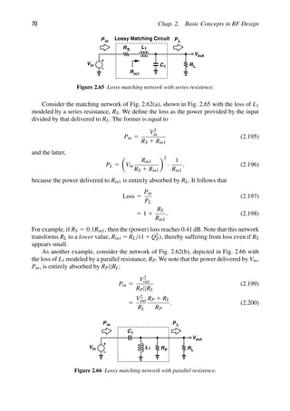
![Sec. 2.7. Analysis of Nonlinear Dynamic Systems 75
Example 2.30 (Continued)
Solution:
Drawing the circuit as shown in Fig. 2.71(b), where CX 5 CGS 1CSB and CY 5 CGD 1CDB,
we write Zin 5 (1/gm)||(CXs)21 and
S11 5
Zin 2 RS
Zin 1 RS
(2.212)
5
1 2 gmRS 2 CXs
1 1 gmRS 1 CXs
. (2.213)
For S12, we recognize that the arrangement of Fig. 2.71(b) yields no coupling from the
output to the input if channel-length modulation is neglected. Thus, S12 5 0. For S22, we
note that Zout 5 RD||(CYs)21 and hence
S22 5
Zout 2 RS
Zout 1 RS
(2.214)
5 2
RS 2 RD 1 RSRDCYs
RS 1 RD 1 RSRDCYs
. (2.215)
Lastly, S21 is obtained according to the configuration of Fig. 2.71(c). Since V2
2 /Vin 5
(V2
2 /VX)(VX/Vin), V2
2 /VX 5 gm[RD||RS||(CYs)21], and VX/Vin 5 Zin/(Zin 1 RS), we
obtain
V2
2
Vin
5 gm
RD||RS||
1
CYs
1
1 1 gmRS 1 RSCXs
. (2.216)
It follows that
S21 5 2gm
RD||RS||
1
CYs
1
1 1 gmRS 1 RSCXs
. (2.217)
2.7 ANALYSIS OF NONLINEAR DYNAMIC SYSTEMS25
In our treatment of systems in Section 2.2, we have assumed a static nonlinearity, e.g., in
the form of y(t) 5 α1x(t)1α2x2(t)1α3x3(t). In some cases, a circuit may exhibit dynamic
nonlinearity, requiring a more complex analysis. In this section, we address this task.
2.7.1 Basic Considerations
Let us first consider a general nonlinear system with an input given by x(t) 5 A1 cos ω1t 1
A2 cos ω2t. We expect the output, y(t), to contain harmonics at nω1, mω2, and IM products
25. This section can be skipped in a first reading.](https://image.slidesharecdn.com/rfmicroelectronicsrazavi-230814101614-71259b59/85/RF-MICROELECTRONICS_Razavi-pdf-100-320.jpg)
![76 Chap. 2. Basic Concepts in RF Design
at kω1 ± qω2, where, n, m, k, and q are integers. In other words,
y(t) 5
∞
n51
an cos(nω1t 1 θn) 1
∞
n51
bn cos(nω2t 1 φn)
1
∞
n52∞
∞
m52∞
cm,n cos(nω1t 1 mω2t 1 φn,m). (2.218)
In the above equation, an, bn, cm,n, and the phase shifts are frequency-dependent quantities.
If the differential equation governing the system is known, we can simply substitute for y(t)
from this expression, equate the like terms, and compute an, bn, cm,n, and the phase shifts.
For example, consider the simple RC section shown in Fig. 2.72, where the capacitor is
nonlinear and expressed as C1 5 C0(11αVout). Adding the voltages across R1 and C1 and
equating the result to Vin, we have
R1C0(1 1 αVout)
dVout
dt
1 Vout 5 Vin. (2.219)
Now suppose Vin(t) 5 V0 cos ω1t1V0 cos ω2t (as in a two-tone test) and assume the system
is only “weakly” nonlinear, i.e., only the output terms at ω1, ω2, ω1 ± ω2, 2ω1 ± ω2, and
2ω2 ± ω1 are significant. Thus, the output assumes the form
Vout(t) 5 a1 cos(ω1t 1 φ1) 1 b1 cos(ω2t 1 φ2) 1 c1 cos[(ω1 1 ω2)t 1 φ3]
1 c2 cos[(ω1 2 ω2)t 1 φ4] 1 c3 cos[(2ω1 1 ω2)t 1 φ5]
1 c4 cos[(ω1 1 2ω2)t 1 φ6] 1 c5 cos[(2ω1 2 ω2)t 1 φ7]
1 c6 cos[(ω1 2 2ω2)t 1 φ8], (2.220)
where, for simplicity, we have used cm and φm. We must now substitute for Vout(t) and
Vin(t) in (2.219), convert products of sinusoids to sums, bring all of the terms to one side of
the equation, group them according to their frequencies, and equate the coefficient of each
sinusoid to zero. We thus obtain a system of 16 nonlinear equations and 16 knowns (a1, b1,
c1, . . ., c6, φ1, . . ., φ8).
R1
C1
out
V
in
V
Figure 2.72 RC circuit with nonlinear capacitor.
This type of analysis is called “harmonic balance” because it predicts the output fre-
quencies and attempts to “balance” the two sides of the circuit’s differential equation by
including these components in Vout(t). The mathematical labor in harmonic balance makes
hand analysis difficult or impossible. The “Volterra series” approach, on the other hand,
prescribes a recursive method that computes the response more accurately in successive](https://image.slidesharecdn.com/rfmicroelectronicsrazavi-230814101614-71259b59/85/RF-MICROELECTRONICS_Razavi-pdf-101-320.jpg)
![Sec. 2.8. Volterra Series 77
steps without the need for solving nonlinear equations. A detailed treatment of the concepts
described below can be found in [10–14].
2.8 VOLTERRA SERIES
In order to understand how the Volterra series represents the time response of a system,
we begin with a simple input form, Vin(t) 5 V0 exp( jω1t). Of course, if we wish to obtain
the response to a sinusoid of the form V0 cos ω1t 5 Re{V0 exp( jω1t)}, we simply cal-
culate the real part of the output.26
(The use of the exponential form greatly simplifies
the manipulation of the product terms.) For a linear, time-invariant system, the output is
given by
Vout(t) 5 H(ω1)V0 exp( jω1t), (2.221)
where H(ω1) is the Fourier transform of the impulse response. For example, if the capacitor
in Fig. 2.72 is linear, i.e., C1 5 C0, then we can substitute for Vout and Vin in Eq. (2.219):
R1C0H(ω1)( jω1)V0 exp( jω1t) 1 H(ω1)V0 exp( jω1t) 5 V0 exp( jω1t). (2.222)
It follows that
H(ω1) 5
1
R1C0 jω1 1 1
. (2.223)
Note that the phase shift introduced by the circuit is included in H(ω1) here.
As our next step, let us ask, how should the output response of a dynamic nonlinear
system be expressed? To this end, we apply two tones to the input, Vin(t) 5 V0 exp( jω1t)1
V0 exp( jω2t), recognizing that the output consists of both linear and nonlinear responses.
The former are of the form
Vout1(t) 5 H(ω1)V0 exp( jω1t) 1 H(ω2)V0 exp( jω2t), (2.224)
and the latter include exponentials such as exp[ j(ω1 1ω2)t], etc. We expect that the coeffi-
cient of such an exponential is a function of both ω1 and ω2. We thus make a slight change
in our notation: we denote H(ωj) in Eq. (2.224) by H1(ωj) [to indicate first-order (linear)
terms] and the coefficient of exp[ j(ω1 1 ω2)t] by H2(ω1, ω2). In other words, the overall
output can be written as
Vout(t) 5 H1(ω1)V0 exp( jω1t) 1 H1(ω2)V0 exp( jω2t)
1 H2(ω1, ω2)V2
0 exp[ j(ω1 1 ω2)t] 1 · · · . (2.225)
How do we determine the terms at 2ω1, 2ω2, and ω1 2 ω2? If H2(ω1, ω2) exp[ j(ω1 1
ω2)t] represents the component at ω1 1 ω2, then H2(ω1, ω1) exp[ j(2ω1)t] must model
26. From another point of view, in V0 exp( jω1t) 5 V0 cos ω1t 1 jV0 sin ω1t, the first term generates its own
response, as does the second term; the two responses remain distinguishable by virtue of the factor j.](https://image.slidesharecdn.com/rfmicroelectronicsrazavi-230814101614-71259b59/85/RF-MICROELECTRONICS_Razavi-pdf-102-320.jpg)
![78 Chap. 2. Basic Concepts in RF Design
that at 2ω1. Similarly, H2(ω2, ω2) and H2(ω1, 2ω2) serve as coefficients for exp[ j(2ω2)t]
and exp[ j(ω1 2 ω2)t], respectively. In other words, a more complete form of Eq. (2.225)
reads
Vout(t) 5 H1(ω1)V0 exp( jω1t) 1 H1(ω2)V0 exp( jω2t) 1 H2(ω1, ω1)V2
0 exp(2jω1t)
1 H2(ω2, ω2)V2
0 exp(2jω2t) 1 H2(ω1, ω2)V2
0 exp[ j(ω1 1 ω2)t]
1 H2(ω1, 2ω2)V2
0 exp[ j(ω1 2 ω2)t] 1 · · · . (2.226)
Thus, our task is simply to compute H2(ω1, ω2).
Example 2.31
Determine H2(ω1, ω2) for the circuit of Fig. 2.72.
Solution:
We apply the input Vin(t) 5 V0 exp( jω1t) 1 V0 exp( jω2t) and assume the output is of the
form Vout(t) 5 H1(ω1)V0 exp( jω1t) 1 H1(ω2)V0 exp( jω2t) 1 H2(ω1, ω2)V2
0 exp[ j(ω1 1
ω2)t]. We substitute for Vout and Vin in Eq. (2.219):
R1C0[1 1 αH1(ω1)V0ejω1t
1 αH1(ω2)V0ejω2t
1 αH2(ω1, ω2)V2
0 ej(ω11ω2)t
]
3 [H1(ω1)jω1V0ejω1t
1 H1(ω2)jω2V0ejω2t
1 H2(ω1, ω2)j(ω1 1 ω2)
3 V2
0 ej(ω11ω2)t
] 1 H1(ω1)ejω1t
1 H1(ω2)ejω2t
1 H2(ω1, ω2)V2
0 ej(ω11ω2)t
5 V0ejω1t
1 V0ejω2t
. (2.227)
To obtain H2, we only consider the terms containing ω1 1 ω2:
R1C0[αH1(ω1)H1(ω2)jω1V2
0 ej(ω11ω2)t
1 αH1(ω2)H1(ω1)jω2V2
0 ej(ω11ω2)t
1 H2(ω1, ω2)j(ω1 1 ω2)V2
0 ej(ω11ω2)t
] 1 H2(ω1, ω2)
3 V2
0 ej(ω11ω2)t
5 0 (2.228)
That is,
H2(ω1, ω2) 5 2
αR1C0 j(ω1 1 ω2)H1(ω1)H1(ω2)
R1C0 j(ω1 1 ω2) 1 1
. (2.229)
Noting that the denominator resembles that of (2.223) but with ω1 replaced by ω1 1ω2,
we simplify H2(ω1, ω2) to
H2(ω1, ω2) 5 2αR1C0 j(ω1 1 ω2)H1(ω1)H1(ω2)H1(ω1 1 ω2). (2.230)
Why did we assume Vout(t) 5 H1(ω1)V0 exp( jω1t) 1 H1(ω2)V0 exp( jω2t) 1
H2V2
0 (ω1, ω2) exp[ j(ω1 1 ω2)t] while we know that Vout(t) also contains terms at
2ω1, 2ω2, and ω1 2 ω2? This is because these other exponentials do not yield terms of the
form exp[ j(ω1 1 ω2)t].](https://image.slidesharecdn.com/rfmicroelectronicsrazavi-230814101614-71259b59/85/RF-MICROELECTRONICS_Razavi-pdf-103-320.jpg)
![Sec. 2.8. Volterra Series 79
Example 2.32
If an input V0 exp( jω1t) is applied to the circuit of Fig. 2.72, determine the amplitude of
the second harmonic at the output.
Solution:
As mentioned earlier, the component at 2ω1 is obtained as H2(ω1, ω1)V2
0 exp[ j(ω1 1ω1)t].
Thus, the amplitude is equal to
|A2ω1| 5 |αR1C0(2ω1)H2
1(ω1)H1(2ω1)|V2
0 (2.231)
5
2|α|R1C0ω1V2
0
(R2
1C2
0ω2
1 1 1)
4R2
1C2
0ω2
1 1 1
. (2.232)
We observe that A2ω1 falls to zero as ω1 approaches zero because C1 draws little current,
and also as ω1 goes to infinity because the second harmonic is suppressed by the low-pass
nature of the circuit.
Example 2.33
If two tones of equal amplitude are applied to the circuit of Fig. 2.72, determine the
ratio of the amplitudes of the components at ω1 1 ω2 and ω1 2 ω2. Recall that H1(ω) 5
(R1C0 jω 1 1)21.
Solution:
From Eq. (2.230), the ratio is given by
Aω11ω2
Aω12ω2
5
H2(ω1, ω2)
H2(ω1, 2ω2)
(2.233)
5
(ω1 1 ω2)H1(ω2)H1(ω1 1 ω2)
(ω1 2 ω2)H1(2ω2)H1(ω1 2 ω2)
. (2.234)
Since |H1(ω2)| 5 |H1(2ω2)|, we have
Aω11ω2
Aω12ω2
5
(ω1 1 ω2)
R2
1C2
0(ω1 2 ω2)2 1 1
|ω1 2 ω2)|
R2
1C2
0(ω1 1 ω2)2 1 1
. (2.235)
The foregoing examples point to a methodical approach that allows us to compute
the second harmonic or second-order IM components with a moderate amount of algebra.
But how about higher-order harmonics or IM products? We surmise that for Nth-order
terms, we must apply the input Vin(t) 5 V0 exp( jω1t) 1 · · · 1 V0 exp( jωNt) and compute
Hn(ω1, . . . , ωn) as the coefficient of the exp[ j(ω1 1 · · · 1 ωn)t] terms in the output. The](https://image.slidesharecdn.com/rfmicroelectronicsrazavi-230814101614-71259b59/85/RF-MICROELECTRONICS_Razavi-pdf-104-320.jpg)
![80 Chap. 2. Basic Concepts in RF Design
output can therefore be expressed as
Vout(t) 5
N
k51
H1(ωk)V0 exp( jωkt) 1
N
m51
N
k51
H2(ωm, ±ωk)V2
0 exp[ j(ωm ± ωk)t]
1
N
n51
N
m51
N
k51
H3(ωn, ±ωm, ±ωk)V3
0 exp[ j(ωn ± ωm ± ωk)t] 1 · · · . (2.236)
The above representation of the output is called the Volterra series. As exemplified by
(2.230), Hm(ω1, . . . , ωm) can be computed in terms of H1, . . . , Hm21 with no need to solve
nonlinear equations. We call Hm the m-th “Volterra kernel.”
Example 2.34
Determine the third Volterra kernel for the circuit of Fig. 2.72.
Solution:
We assume Vin(t) 5 V0 exp( jω1t) 1 V0 exp( jω2t) 1 V0 exp( jω3t). Since the output con-
tains many components, we introduce the short hands H1(1) 5 H1(ω1)V0 exp( jω1t),
H1(2) 5 H1(ω2)V0 exp( jω2t), etc., H2(1,2) 5 H2(ω1, ω2)V2
0 exp[ j(ω1 1 ω2)t], etc., and
H3(1,2,3) 5 H3(ω1, ω2, ω3)V3
0 exp[ j(ω1 1 ω2 1 ω3)t]. We express the output as
Vout(t) 5 H1(1) 1 H1(2) 1 H1(3) 1 H2(1,2) 1 H2(1,3) 1 H2(2,3) 1 H2(1,1)
1 H2(2,2) 1 H2(3,3) 1 H3(1,2,3) 1 · · · . (2.237)
We must substitute for Vout and Vin in Eq. (2.219) and group all of the terms that con-
tain ω1 1 ω2 1 ω3. To obtain such terms in the product of αVout and dVout/dt, we
note that αH2(1,2)jω3H1(3) and αH1(3)j(ω1 1 ω2)H2(1,2) produce an exponential of the
form exp[ j(ω1 1 ω2)t] exp( jω3). Similarly, αH2(2,3)jω1H1(1), αH1(1)j(ω2 1 ω3)H2(2,3),
αH2(1,3)jω2H1(2), and αH1(2)j(ω1 1 ω3)H2(1,3) result in ω1 1 ω2 1 ω3. Finally, the product
of αVout and dVout/dt also contains 1 3 j(ω1 1 ω2 1 ω3)H3(1,2,3). Grouping all of the
terms, we have
H3(ω1, ω2, ω3)
5 2jαR1C0
H2(ω1, ω2)ω3H1(ω3) 1 H2(ω2, ω3)ω1H1(ω1) 1 H2(ω1, ω3)ω2H1(ω2)
R1C0 j(ω1 1 ω2 1 ω3) 1 1
2 jαR1C0
H1(ω1)(ω2 1 ω3)H2(ω2, ω3) 1 H1(ω2)(ω1 1 ω3)H2(ω1, ω3)
R1C0 j(ω1 1 ω2 1 ω3) 1 1
2 jαR1C0
H1(ω3)(ω1 1 ω2)H2(ω1, ω2)
R1C0 j(ω1 1 ω2 1 ω3) 1 1
. (2.238)
Note that H2(1,1), etc., do not appear here and could have been omitted from Eq. (2.237).
With the third Volterra kernel available, we can compute the amplitude of critical terms.
For example, the third-order IM components in a two-tone test are obtained by substituting
ω1 for ω3 and 2ω2 for ω2.](https://image.slidesharecdn.com/rfmicroelectronicsrazavi-230814101614-71259b59/85/RF-MICROELECTRONICS_Razavi-pdf-105-320.jpg)
![Sec. 2.8. Volterra Series 81
The reader may wonder if the Volterra series can be used with inputs other than
exponentials. This is indeed possible [14] but beyond the scope of this book.
The approach described in this section is called the “harmonic” method of kernel
calculation. In summary, this method proceeds as follows:
1. Assume Vin(t) 5 V0 exp( jω1t) and Vout(t) 5 H1(ω1)V0 exp( jω1t). Substitute for
Vout and Vin in the system’s differential equation, group the terms that contain
exp( jω1t), and compute the first (linear) kernel, H1(ω1).
2. Assume Vin(t) 5 V0 exp( jω1t)1V0 exp( jω2t) and Vout(t) 5 H1(ω1)V0 exp( jω1t)1
H1(ω2)V0 exp( jω2t) 1 H2(ω1, ω2)V2
0 exp[ j(ω1 1 ω2)t]. Make substitutions in the
differential equation, group the terms that contain exp[ j(ω1 1 ω2)t], and determine
the second kernel, H2(ω1, ω2).
3. Assume Vin(t) 5 V0 exp( jω1t) 1 V0 exp( jω2t) 1 V0 exp( jω3t) and Vout(t) is given
by Eq. (2.237). Make substitutions, group the terms that contain exp[ j(ω1 1 ω2 1
ω3)t], and calculate the third kernel, H3(ω1, ω2, ω3).
4. To compute the amplitude of harmonics and IM components, choose ω1, ω2, . . .
properly. For example, H2(ω1, ω1) yields the transfer function for 2ω1 and
H3(ω1, 2ω2, ω1) the transfer function for 2ω1 2 ω2.
2.8.1 Method of Nonlinear Currents
As seen in Example 2.34, the harmonic method becomes rapidly more complex as n
increases. An alternative approach called the method of “nonlinear currents” is sometimes
preferred as it reduces the algebra to some extent. We describe the method itself here and
refer the reader to [13] for a formal proof of its validity.
The method of nonlinear currents proceeds as follows for a circuit that contains a two-
terminal nonlinear device [13]:
1. Assume Vin(t) 5 V0 exp( jω1t) and determine the linear response of the circuit by
ignoring the nonlinearity. The “response” includes both the output of interest and
the voltage across the nonlinear device.
2. Assume Vin(t) 5 V0 exp( jω1t) 1 V0 exp( jω2t) and calculate the voltage across the
nonlinear device, assuming it is linear. Now, compute the nonlinear component of
the current flowing through the device, assuming the device is nonlinear.
3. Set the main input to zero and place a current source equal to the nonlinear
component found in Step 2 in parallel with the nonlinear device.
4. Ignoring the nonlinearity of the device again, determine the circuit’s response to the
current source applied in Step 3. Again, the response includes the output of interest
and the voltage across the nonlinear device.
5. Repeat Steps 2, 3, and 4 for higher-order responses. The overall response is equal
to the output components found in Steps 1, 4, etc.
The following example illustrates the procedure.](https://image.slidesharecdn.com/rfmicroelectronicsrazavi-230814101614-71259b59/85/RF-MICROELECTRONICS_Razavi-pdf-106-320.jpg)
![82 Chap. 2. Basic Concepts in RF Design
Example 2.35
Determine H3(ω1, ω2, ω3) for the circuit of Fig. 2.72.
Solution:
In this case, the output voltage also appears across the nonlinear device. We know that
H1(ω1) 5 (R1C0 jω1 1 1)21. Thus, with Vin(t) 5 V0 exp( jω1t), the voltage across the
capacitor is equal to
VC1(t) 5
V0
R1C0 jω1 1 1
ejω1t
. (2.239)
In the second step, we apply Vin(t) 5 V0 exp( jω1t) 1 V0 exp( jω2t), obtaining the linear
voltage across C1 as
VC1(t) 5
V0ejω1t
R1C0 jω1 1 1
1
V0ejω2t
R1C0 jω2 1 1
. (2.240)
With this voltage, we compute the nonlinear current flowing through C1:
IC1,non(t) 5 αC0VC1
dVC1
dt
(2.241)
5 αC0
V0ejω1t
R1C0jω1 1 1
1
V0ejω2t
R1C0 jω2 1 1
3
jω1V0ejω1t
R1C0 jω1 1 1
1
jω2V0ejω2t
R1C0 jω2 1 1
. (2.242)
Since only the component at ω1 1 ω2 is of interest at this point, we rewrite the above
expression as
IC1,non(t) 5 αC0
j(ω1 1 ω2)V2
0 ej(ω11ω2)t
(R1C0 jω1 1 1)(R1C0 jω2 1 1)
1 · · ·
(2.243)
5 αC0[ j(ω1 1 ω2)V2
0 ej(ω11ω2)t
H1(ω1)H1(ω2) 1 · · · ]. (2.244)
In the third step, we set the input to zero, assume a linear capacitor, and apply IC1,non(t) in
parallel with C1 (Fig. 2.73). The current component at ω1 1 ω2 flows through the parallel
combination of R1 and C0, producing VC1,non(t):
R1
C
out
V
0 I C1,non
Figure 2.73 Inclusion of nonlinear current in RC section.](https://image.slidesharecdn.com/rfmicroelectronicsrazavi-230814101614-71259b59/85/RF-MICROELECTRONICS_Razavi-pdf-107-320.jpg)
![Sec. 2.8. Volterra Series 83
Example 2.35 (Continued)
VC1,non(t) 5 2αC0 j(ω1 1 ω2)V2
0 ej(ω11ω2)t
H1(ω1)
3 H1(ω2)
R1
R1C0j(ω1 1 ω2) 1 1
(2.245)
5 2αR1C0 j(ω1 1 ω2)H1(ω1)H1(ω2)H1(ω1 1 ω2)V2
0 ej(ω11ω2)t
. (2.246)
We note that the coefficient of V2
0 exp[ j(ω1 1 ω2)t] in these two equations is the same as
H2(ω1, ω2) in (2.229).
To determine H3(ω1, ω2, ω3), we must assume an input of the form Vin(t) 5
V0 exp( jω1t) 1 V0 exp( jω2t) 1 V0 exp( jω3t) and write the voltage across C1 as
VC1(t) 5 H1(ω1)V0ejω1t
1 H1(ω2)V0ejω2t
1 H1(ω3)V0ejω3t
1 H2(ω1, ω2)V2
0 ej(ω11ω2)t
1 H2(ω1, ω3)V2
0 ej(ω11ω3)t
1 H2(ω2, ω3)V2
0 ej(ω21ω3)t
. (2.247)
Note that, in contrast to Eq. (2.240), we have included the second-order nonlinear terms in
the voltage so as to calculate the third-order terms.27
The nonlinear current through C1 is
thus equal to
IC1,non(t) 5 αC0VC1
dVC1
dt
. (2.248)
We substitute for VC1 and group the terms containing ω1 1 ω2 1 ω3:
IC1,non(t) 5 αC0[H1(ω1)H2(ω2, ω3)j(ω2 1 ω3) 1 H2(ω2, ω3)jω1H1(ω1)
1 H1(ω2)H2(ω1, ω3)j(ω1 1 ω3) 1 H2(ω1, ω3)jω2H1(ω2)
1 H1(ω3)H2(ω1, ω2)j(ω1 1 ω2) 1 H2(ω1, ω2)jω3H1(ω3)]V3
0 ej(ω11ω21ω3)t
1 · · · . (2.249)
This current flows through the parallel combination of R1 and C0, yielding VC1,non(t). The
reader can readily show that the coefficient of exp[ j(ω1 1 ω2 1 ω3)t] in VC1,non(t) is the
same as the third kernel expressed by Eq. (2.238).
The procedure described above applies to two-terminal nonlinear devices. For transis-
tors, a similar approach can be taken. We illustrate this point with the aid of an example.
Example 2.36
Figure 2.74(a) shows the input network of a commonly-used LNA (Chapter 5). Assuming
that gmL1/CGS 5 RS (Chapter 5) and ID 5 α(VGS 2 VTH)2, determine the nonlinear terms
in Iout. Neglect other capacitances, channel-length modulation, and body effect.
(Continues)
27. Other terms are excluded because they do not lead to a component at ω1 1 ω2 1 ω3.](https://image.slidesharecdn.com/rfmicroelectronicsrazavi-230814101614-71259b59/85/RF-MICROELECTRONICS_Razavi-pdf-108-320.jpg)
![84 Chap. 2. Basic Concepts in RF Design
Example 2.36 (Continued)
M 1
L1
CGS V1
LG
Vin
RS
I out
M 1
L1
CGS V1
LG
RS
I out
I D,non
L1
CGS
V1
LG
RS
I D,non
g
m
V1
I out
(a) (b)
(c)
Figure 2.74 (a) CS stage with inductors in series with source and gate, (b) inclusion of nonlinear
current, (c) computation of output current.
Solution:
In this circuit, two quantities are of interest, namely, the output current, Iout ( 5 ID), and
the gate-source voltage, V1; the latter must be computed each time as it determines the
nonlinear component in ID.
Let us begin with the linear response. Since the current flowing through L1 is equal to
V1CGSs 1 gmV1 and that flowing through RS and LG equal to V1CGSs, we can write a KVL
around the input loop as
Vin 5 (RS 1 LGs)V1CGSs 1 V1 1 (V1CGSs 1 gmV1)L1s. (2.250)
It follows that
V1
Vin
5
1
(L1 1 LG)CGSs2 1 (RSCGS 1 gmL1)s 1 1
. (2.251)
Since we have assumed gmL1/CGS 5 RS, for s 5 jω we obtain
V1
Vin
( jω) 5
1
2gmL1jω 1 1 2
ω2
ω2
0
5 H1(ω), (2.252)
where ω2
0 5 [(L1 1 LG)CGS]21. Note that Iout 5 gmV1 5 gmH1(ω)Vin.](https://image.slidesharecdn.com/rfmicroelectronicsrazavi-230814101614-71259b59/85/RF-MICROELECTRONICS_Razavi-pdf-109-320.jpg)
![Sec. 2.8. Volterra Series 85
Example 2.36 (Continued)
Now, we assume Vin(t) 5 V0 exp( jω1t) 1 V0 exp( jω2t) and write
V1(t) 5 H1(ω1)V0ejω1t
1 H1(ω2)V0ejω2t
. (2.253)
Upon experiencing the characteristic ID 5 αV2
1 , this voltage results in a nonlinear current
given by
ID,non 5 2αH1(ω1)H1(ω2)V2
0 ej(ω11ω2)t
. (2.254)
In the next step, we set Vin to zero and insert a current source having the above value in
parallel with the drain current source [Fig. 2.74(b)]. We must compute V1 in response to
ID,non, assuming the circuit is linear. From the equivalent circuit shown in Fig. 2.74(c), we
have the following KVL:
(RS 1 LGs)V1CGSs 1 V1 1 (gmV1 1 ID,non 1 V1CGSs)L1s 5 0. (2.255)
Thus, for s 5 jω
V1
ID,non
( jω) 5
2jL1ω
2gmL1jω 1 1 2
ω2
ω2
0
. (2.256)
Since ID,non contains a frequency component at ω1 1 ω2, the above transfer function must
be calculated at ω1 1 ω2 and multiplied by ID,non to yield V1. We therefore have
H2(ω1, ω2) 5
2jL1(ω1 1 ω2)
2gmL1j(ω1 1 ω2) 1 1 2
(ω1 1 ω2)2
ω2
0
2αH1(ω1)H1(ω2). (2.257)
In our last step, we assume Vin(t) 5 V0 exp( jω1t)1V0 exp( jω2t)1V0 exp( jω3t) and write
V1(t) 5 H1(ω1)V0ejω1t
1 H1(ω2)V0ejω2t
1 H1(ω3)V0ejω3t
1 H2(ω1, ω2)V2
0 ej(ω11ω2)t
1 H2(ω1, ω3)V2
0 ej(ω11ω3)t
1 H2(ω2, ω3)V2
0 ej(ω21ω3)t
. (2.258)
Since ID 5 αV2
1 , the nonlinear current at ω1 1 ω2 1 ω3 is expressed as
ID,non 5 2α[H1(ω1)H2(ω2, ω3) 1 H1(ω2)H2(ω1, ω3)
1 H1(ω3)H2(ω1, ω2)]V3
0 ej(ω11ω21ω3)t
. (2.259)
The third-order nonlinear component in the output of interest, Iout, is equal to the
above expression. We note that, even though the transistor exhibits only second-order
nonlinearity, the degeneration (feedback) caused by L1 results in higher-order terms.
The reader is encouraged to repeat this analysis using the harmonic method and see
that it is much more complex.](https://image.slidesharecdn.com/rfmicroelectronicsrazavi-230814101614-71259b59/85/RF-MICROELECTRONICS_Razavi-pdf-110-320.jpg)
![86 Chap. 2. Basic Concepts in RF Design
REFERENCES
[1] B. Razavi, Design of Analog CMOS Integrated Circuits, Boston: McGraw-Hill, 2001.
[2] L. W. Couch, Digital and Analog Communication Systems, Fourth Edition, New York:
Macmillan Co., 1993.
[3] A. van der Ziel, “Thermal Noise in Field Effect Transistors,” Proc. IRE, vol. 50, pp. 1808–1812,
Aug. 1962.
[4] A. A. Abidi, “High-Frequency Noise Measurements on FETs with Small Dimensions,” IEEE
Trans. Electron Devices, vol. 33, pp. 1801–1805, Nov. 1986.
[5] A. J. Sholten et al., “Accurate Thermal Noise Model of Deep-Submicron CMOS,” IEDM Dig.
Tech. Papers, pp. 155–158, Dec. 1999.
[6] B. Razavi, “Impact of Distributed Gate Resistance on the Performance of MOS Devices,”
IEEE Trans. Circuits and Systems- Part I, vol. 41, pp. 750–754, Nov. 1994.
[7] H. T. Friis, “Noise Figure of Radio Receivers,” Proc. IRE, vol. 32, pp. 419–422, July 1944.
[8] A. Papoulis, Probability, Random Variables, and Stochastic Processes, Third Edition, New
York: McGraw-Hill, 1991.
[9] R. W. Bennet, “Methods of Solving Noise Problems,” Proc. IRE, vol. 44, pp. 609–638, May
1956.
[10] S. Narayanan, “Application of Volterra Series to Intermodulation Distortion Analysis of
Transistor Feedback Amplifiers,” IEEE Tran. Circuit Theory, vol. 17, pp. 518–527, Nov. 1970.
[11] P. Wambacq et al., “High-Frequency Distortion Analysis of Analog Integrated Circuits,” IEEE
Tran. Circuits and Systems, II, vol. 46, pp. 335–334, March 1999.
[12] P. Wambaq and W. Sansen, Distortion Analysis of Analog Integrated Circuits, Norwell, MA:
Kluwer, 1998.
[13] J. Bussganag, L. Ehrman, and J. W. Graham, “Analysis of Nonlinear Systems with Multiple
Inputs,” Proc. IEEE, vol. 62, pp. 1088–1119, Aug. 1974.
[14] E. Bedrosian and S. O. Rice, “The Output Properties of Volterra Systems (Nonlinear Systems
with Memory) Driven by Harmonic and Gaussian Inputs,” Proc. IEEE, vol. 59, pp. 1688–
1707, Dec. 1971.
PROBLEMS
2.1. Two nonlinear stages are cascaded. If the input/output characteristic of each stage
is approximated by a third-order polynomial, determine the P1dB of the cascade in
terms of the P1dB of each stage.
2.2. Repeat Example 2.11 if one interferer has a level of 23 dBm and the other, 235 dBm.
2.3. If cascaded, stages having only second-order nonlinearity can yield a finite IP3. For
example, consider the cascade identical common-source stages shown in Fig. 2.75.
RD
VDD
M 1
RD
M 2
in
V
out
V
Figure 2.75 Cascade of CS stages.](https://image.slidesharecdn.com/rfmicroelectronicsrazavi-230814101614-71259b59/85/RF-MICROELECTRONICS_Razavi-pdf-111-320.jpg)
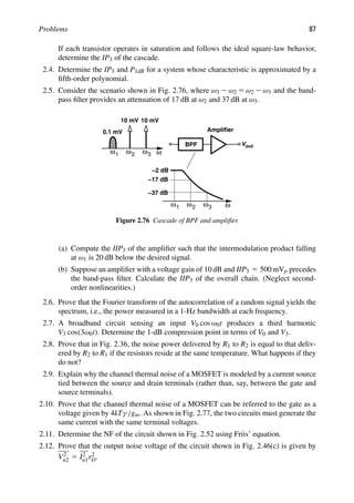
![88 Chap. 2. Basic Concepts in RF Design
I n
2
M 1
I D
V1
V2
V3
M 1
I D
V1
V2
V3
V 2
n
Figure 2.77 Equivalent circuits for noise of a MOSFET.
2.13. Repeat Example 2.23 if the CS and CG stages are swapped. Does the NF change?
Why?
2.14. Repeat Example 2.23 if RD1 and RD2 are replaced with ideal current sources and
channel-length modulation is not neglected.
2.15. The input/output characteristic of a bipolar differential pair is given by Vout 5
22RCIEE tanh[Vin/(2VT)], where RC denotes the load resistance, IEE is the tail
current, and VT 5 kT/q. Determine the IP3 of the circuit.
2.16. What happens to the noise figure of a circuit if the circuit is loaded by a noiseless
impedance ZL at its output?
2.17. The noise figure of a circuit is known for a source impedance of RS1. Is it possible to
compute the noise figure for another source impedance RS2? Explain in detail.
2.18. Equation (2.122) implies that the noise figure falls as RS rises. Assuming that the
antenna voltage swing remains constant, explain what happens to the output SNR as
RS increases.
2.19. Repeat Example 2.21 for the arrangement shown in Fig. 2.78, where the transformer
amplifies its primary voltage by a factor of n and transforms RS to a value of n2RS.
VDD
M
I 1
1
RS
Vin
1:n
out
V
Figure 2.78 CS stage driven by a transformer.
2.20. For matched inputs and outputs, prove that the NF of a passive (reciprocal) circuit is
equal to its power loss.
2.21. Determine the noise figure of each circuit in Fig. 2.79 with respect to a source
impedance RS. Neglect channel-length modulation and body effect.](https://image.slidesharecdn.com/rfmicroelectronicsrazavi-230814101614-71259b59/85/RF-MICROELECTRONICS_Razavi-pdf-113-320.jpg)
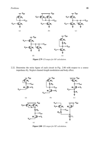
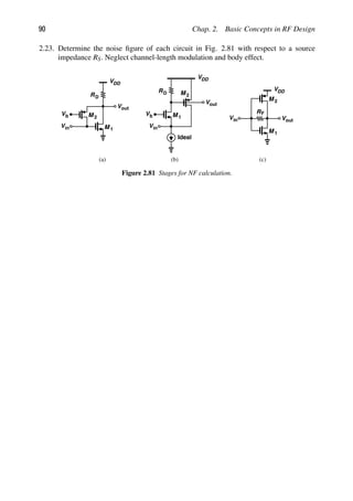
![CHAPTER
3
COMMUNICATION CONCEPTS
The design of highly-integrated RF transceivers requires a solid understanding of commu-
nication theory. For example, as mentioned in Chapter 2, the receiver sensitivity depends
on the minimum acceptable signal-to-noise ratio, which itself depends on the type of mod-
ulation. In fact, today we rarely design a low-noise amplifier, an oscillator, etc., with no
attention to the type of transceiver in which they are used. Furthermore, modern RF design-
ers must regularly interact with digital signal processing engineers to trade functions and
specifications and must therefore speak the same language.
This chapter provides a basic, yet necessary, understanding of modulation theory and
wireless standards. Tailored to a reader who is ultimately interested in RF IC design rather
than communication theory, the concepts are described in an intuitive language so that they
can be incorporated in the reader’s daily work. The outline of the chapter is shown below.
Modulation
AM, PM, FM
Intersymbol Interference
Signal Constellations
ASK, PSK, FSK
QPSK, GMSK, QAM
OFDM
Spectral Regrowth
Mobile Systems
Cellular System
Hand-off
Multipath Fading
Diversity
Multiple Access Technqiues
Duplexing
FDMA
TDMA
CDMA
Wireless Standards
GSM
IS−95 CDMA
Wideband CDMA
Bluetooth
IEEE802.11a/b/g
3.1 GENERAL CONSIDERATIONS
How does your voice enter a cell phone here and come out of another cell phone miles
away? We wish to understand the incredible journey that your voice signal takes.
The transmitter in a cell phone must convert the voice, which is called a “baseband
signal” because its spectrum (20 Hz to 20 kHz) is centered around zero frequency, to a
“passband signal,” i.e., one residing around a nonzero center frequency, ωc [Fig. 3.1(b)].
We call ωc the “carrier frequency.”
91](https://image.slidesharecdn.com/rfmicroelectronicsrazavi-230814101614-71259b59/85/RF-MICROELECTRONICS_Razavi-pdf-116-320.jpg)
![92 Chap. 3. Communication Concepts
0
0 w wc wc w
(a) (b)
Figure 3.1 (a) Baseband and (b) passband signal spectra.
More generally, “modulation” converts a baseband signal to a passband signal. From
another point of view, modulation varies certain parameters of a sinusoidal carrier accord-
ing to the baseband signal. For example, if the carrier is expressed as A0 cos ωct, then the
modulated signal is given by
x(t) 5 a(t) cos[ωct 1 θ(t)], (3.1)
where the amplitude, a(t) and the phase, θ(t), are modulated.
The inverse of modulation is demodulation or detection, with the goal being to recon-
struct the original baseband signal with minimal noise, distortion, etc. Thus, as depicted
in Fig. 3.2, a simple communication system consists of a modulator/transmitter, a chan-
nel (e.g., air or a cable), and a receiver/demodulator. Note that the channel attenuates the
signal. A “transceiver” contains both a modulator and a demodulator; the two are called a
“modem.”
Baseband
Signal
Modulator Channel Demodulator
Detected
Signal
Transmitter Receiver
Figure 3.2 Generic communication system.
Important Aspects of Modulation Among various attributes of each modulation scheme,
three prove particularly critical in RF design.
1. Detectability, i.e., the quality of the demodulated signal for a given amount of
channel attenuation and receiver noise. As an example, consider the binary ampli-
tude modulation shown in Fig. 3.3(a), where logical ONEs are represented by full
amplitude and ZEROs by zero amplitude. The demodulation must simply distin-
guish between these two amplitude values. Now, suppose we wish to carry more
information and hence employ four different amplitudes as depicted in Fig. 3.3(b).
t t
(a) (b)
1 0 1 01 10 11 00
Figure 3.3 (a) Two-level and (b) four-level modulation schemes.](https://image.slidesharecdn.com/rfmicroelectronicsrazavi-230814101614-71259b59/85/RF-MICROELECTRONICS_Razavi-pdf-117-320.jpg)
![Sec. 3.2. Analog Modulation 93
In this case, the four amplitude values are closer to one another and can therefore be
misinterpreted in the presence of noise. We say the latter signal is less detectable.
2. Bandwidth efficiency, i.e., the bandwidth occupied by the modulated carrier for
a given information rate in the baseband signal. This aspect plays a critical role
in today’s systems because the available spectrum is limited. For example, the
GSM phone system provides a total bandwidth of 25 MHz for millions of users
in crowded cities. The sharing of this bandwidth among so many users is explained
in Section 3.6.
3. Power efficiency, i.e., the type of power amplifier (PA) that can be used in the
transmitter. As explained later in this chapter, some modulated waveforms can be
processed by means of nonlinear power amplifiers, whereas some others require
linear amplifiers. Since nonlinear PAs are generally more efficient (Chapter 12),
it is desirable to employ a modulation scheme that lends itself to nonlinear
amplification.
The above three attributes typically trade with one another. For example, we may suspect
that the modulation format in Fig. 3.3(b) is more bandwidth-efficient than that in Fig. 3.3(a)
because it carries twice as much information for the same bandwidth. This advantage comes
at the cost of detectability—because the amplitude values are more closely spaced—and
power efficiency—because PA nonlinearity compresses the larger amplitudes.
3.2 ANALOG MODULATION
If an analog signal, e.g., that produced by a microphone, is impressed on a carrier, then we
say we have performed analog modulation. While uncommon in today’s high-performance
communications, analog modulation provides fundamental concepts that prove essential in
studying digital modulation as well.
3.2.1 Amplitude Modulation
For a baseband signal xBB(t), an amplitude-modulated (AM) waveform can be construc-
ted as
xAM(t) 5 Ac[1 1 mxBB(t)] cos ωct, (3.2)
where m is called the “modulation index.”1
Illustrated in Fig. 3.4(a) is a multiplication
method for generating an AM signal. We say the baseband signal is “upconverted.” The
waveform Ac cos ωct is generated by a “local oscillator” (LO). Multiplication by cos ωct
in the time domain simply translates the spectrum of xBB(t) to a center frequency of ωc
[Fig. 3.4(b)]. Thus, the bandwidth of xAM(t) is twice that of xBB(t). Note that since xBB(t)
has a symmetric spectrum around zero (because it is a real signal), the spectrum of xAM(t)
is also symmetric around ωc. This symmetry does not hold for all modulation schemes and
plays a significant role in the design of transceiver architectures (Chapter 4).
1. Note that m has a dimension of 1/volt if xBB(t) is a voltage quantity.](https://image.slidesharecdn.com/rfmicroelectronicsrazavi-230814101614-71259b59/85/RF-MICROELECTRONICS_Razavi-pdf-118-320.jpg)
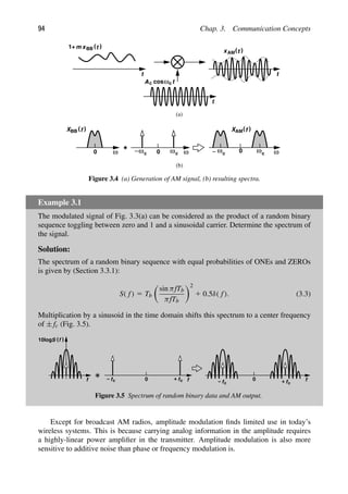
![Sec. 3.2. Analog Modulation 95
3.2.2 Phase and Frequency Modulation
Phase modulation (PM) and frequency modulation (FM) are important concepts that are
encountered not only within the context of modems but also in the analysis of such circuits
as oscillators and frequency synthesizers.
Let us consider Eq. (3.1) again. We call the argument ωct 1 θ(t) the “total phase.”
We also define the “instantaneous frequency” as the time derivative of the phase; thus,
ωc 1 dθ/dt is the “total frequency” and dθ/dt is the “excess frequency” or the “frequency
deviation.” If the amplitude is constant and the excess phase is linearly proportional to the
baseband signal, we say the carrier is phase-modulated:
xPM(t) 5 Ac cos[ωct 1 mxBB(t)], (3.4)
where m denotes the phase modulation index. To understand PM intuitively, first note that,
if xBB(t) 5 0, then the zero-crossing points of the carrier waveform occur at uniformly-
spaced instants equal to integer multiples of the period, Tc 5 1/ωc. For a time-varying
xBB(t), on the other hand, the zero crossings are modulated (Fig. 3.6) while the amplitude
remains constant.
t
)
(t
xPM
Figure 3.6 Zero crossings in a phase-modulated signal.
Similarly, if the excess frequency, dθ/dt, is linearly proportional to the baseband signal,
we say the carrier is frequency-modulated:
xFM(t) 5 Ac cos[ωct 1 m
t
2∞
xBB(τ)dτ]. (3.5)
Note that the instantaneous frequency is equal to ωc 1 mxBB(t).2
Example 3.2
Determine the PM and FM signals in response to (a) xBB(t) 5 A0, (b) xBB(t) 5 αt.
Solution:
(a) For a constant baseband signal,
xPM(t) 5 Ac cos(ωct 1 mA0); (3.6)
(Continues)
2. In this case, m has a dimension of radian frequency/volt if xBB(t) is a voltage quantity.](https://image.slidesharecdn.com/rfmicroelectronicsrazavi-230814101614-71259b59/85/RF-MICROELECTRONICS_Razavi-pdf-120-320.jpg)
![96 Chap. 3. Communication Concepts
Example 3.2 (Continued)
i.e., the PM output simply contains a constant phase shift. The FM output, on the other
hand, is expressed as
xFM(t) 5 Ac cos(ωct 1 mA0t) (3.7)
5 Ac cos[(ωc 1 mA0)t]. (3.8)
Thus, the FM output exhibits a constant frequency shift equal to mA0.
(b) If xBB(t) 5 αt, then
xPM(t) 5 Ac cos(ωct 1 mαt) (3.9)
5 Ac cos[(ωc 1 mα)t], (3.10)
i.e., the PM output experiences a constant frequency shift. For the FM output, we have,
xFM(t) 5 Ac cos
ωct 1
mα
2
t2
. (3.11)
This signal can be viewed as a waveform whose phase grows quadratically with time.
The nonlinear dependence of xPM(t) and xFM(t) upon xBB(t) generally increases the
occupied bandwidth. For example, if xBB(t) 5 Am cos ωmt, then
xFM(t) 5 Ac cos
ωct 1
mAm
ωm
sin ωmt
, (3.12)
exhibiting spectral lines well beyond ωc ± ωm. Various approximations for the bandwidth
of PM and FM signals have been derived [1–3].
Narrowband FM Approximation A special case of FM that proves useful in the analysis
of RF circuits and systems arises if mAm/ωm 1 rad in Eq. (3.12). The signal can then be
approximated as
xFM(t) ≈ Ac cos ωct 2 AmAc
m
ωm
sin ωmt sin ωct (3.13)
≈ Ac cos ωct 2
mAmAc
2ωm
cos(ωc 2 ωm)t 1
mAmAc
2ωm
cos(ωc 1 ωm)t. (3.14)
Illustrated in Fig. 3.7, the spectrum consists of impulses at ±ωc (the carrier) and “side-
bands” at ωc ± ωm and 2ωc ± ωm. Note that, as the modulating frequency, ωm, increases,
the magnitude of the sidebands decreases.](https://image.slidesharecdn.com/rfmicroelectronicsrazavi-230814101614-71259b59/85/RF-MICROELECTRONICS_Razavi-pdf-121-320.jpg)
![Sec. 3.2. Analog Modulation 97
ω
0
ω
ω
ω
ω
m m
ωc
m
ωc
ωm
ωc
)
(
BB FM
X f X ( )
f
0
ω
ωc
m
ωc
ωm
ωc
Figure 3.7 Spectrum of a narrowband FM signal.
Example 3.3
It is sometimes said that the FM (or PM) sidebands have opposite signs, whereas AM
sidebands have identical signs. Is this generally true?
Solution:
Equation (3.14) indeed suggests that cos(ωc 2ωm)t and cos(ωc 1ωm)t have opposite signs.
Figure 3.8(a) illustrates this case by allowing signs in the magnitude plot. For a carrier
whose amplitude is modulated by a sinusoid, we have
xAM(t) 5 Ac(1 1 m cos ωmt) cos ωct (3.15)
5 Ac cos ωct 1
mAc
2
cos(ωc 1 ωm)t 1
mAc
2
cos(ωc 2 ωm)t. (3.16)
Thus, it appears that the sidebands have identical signs [Fig. 3.8(b)]. However, in general,
the polarity of the sidebands per se does not distinguish AM from FM. Writing the four
possible combinations of sine and cosine in Eqs. (3.2) and (3.5), the reader can arrive at
the spectra shown in Fig. 3.9. Given the exact waveforms for the carrier and the sidebands,
one can decide from these spectra whether the modulation is AM or narrowband FM.
ω
ω
ωc
m
ωc
ωm
ωc
ω
ω
ωc
m
ωc
ωm
ωc
(a) (b)
Figure 3.8 Spectra of (a) narrowband FM and (b) AM signals.
However, an important difference between the AM and FM sidebands relates to their
angular rotation with respect to the carrier. In an AM signal, the sidebands must modulate
only the amplitude at any time. Thus, as illustrated by phasors in Fig. 3.10(a), the two must
rotate in opposite directions such that their resultant remains aligned with the carrier. On
the other hand, the sidebands of an FM signal must create no component along the carrier
amplitude, and hence are positioned as shown in Fig. 3.10(b) so that their resultant remains
perpendicular to the carrier at all times.
(Continues)](https://image.slidesharecdn.com/rfmicroelectronicsrazavi-230814101614-71259b59/85/RF-MICROELECTRONICS_Razavi-pdf-122-320.jpg)
![98 Chap. 3. Communication Concepts
Example 3.3 (Continued)
ω0 ω ω0 ω
cosine
cosine
cosine
cosine
sine
sine
ω0 ω
sine
cosine
cosine
ω0 ω
sine sine
cosine
ω0 ω
cosine
sine sine
ω0 ω
cosine
cosine
cosine
ω0 ω
sine
sine
sine
ω0 ω
sine
cosine
cosine
AM
NBFM
Figure 3.9 Spectra of AM and narrowband FM signals.
ω
Carrier
c
AM Sideband
AM Sideband
Resultant
ω
Carrier
c
Resultant
FM Sideband
FM Sideband
(a) (b)
Figure 3.10 Rotation of (a) AM and (b) FM sidebands with respect to the carrier.
The insights afforded by the above example prove useful in many RF circuits. The
following example shows how an interesting effect in nonlinear circuits can be explained
with the aid of the foregoing observations.
Example 3.4
The sum of a large sinusoid at ωc and a small sinusoid at ωc 1ωm is applied to a differential
pair [Fig. 3.11(a)]. Explain why the output spectrum contains a component at ωc 2 ωm.
Assume that the differential pair experiences “hard limiting,” i.e., A is large enough to steer
ISS to each side.
Solution:
Let us decompose the input spectrum into two symmetric spectra as shown in Fig. 3.11(b).3
The one with sidebands of identical signs can be viewed as an AM waveform, which, due
to hard limiting, is suppressed at the output. The spectrum with sidebands of opposite
3. We call these symmetric because omission of sideband signs would make them symmetric.](https://image.slidesharecdn.com/rfmicroelectronicsrazavi-230814101614-71259b59/85/RF-MICROELECTRONICS_Razavi-pdf-123-320.jpg)
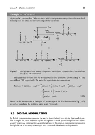
![Sec. 3.3. Digital Modulation 101
3.3.1 Intersymbol Interference
Linear time-invariant systems can “distort” a signal if they do not provide sufficient
bandwidth. A familiar example of such a behavior is the attenuation of high-frequency
components of a periodic square wave in a low-pass filter [Fig. 3.14(a)]. However, lim-
ited bandwidth more detrimentally impacts random bit streams. To understand the issue,
first recall that if a single ideal rectangular pulse is applied to a low-pass filter, then the
output exhibits an exponential tail that becomes longer as the filter bandwidth decreases.
This occurs fundamentally because a signal cannot be both time-limited and bandwidth-
limited: when the time-limited pulse passes through the band-limited system, the output
must extend to infinity in the time domain.
C
R1
1
in
V
Vout
t
t
t
Vout
in
V out
V
(a)
(b)
Figure 3.14 Effect of low-pass filter on (a) periodic waveform and (b) random sequence.
Now suppose the output of a digital system consists of a random sequence of ONEs and
ZEROs. If this sequence is applied to a low-pass filter (LPF), the output can be obtained as
the superposition of the responses to each input bit [Fig. 3.14(b)]. We note that each bit level
is corrupted by decaying tails created by previous bits. Called “intersymbol interference”
(ISI), this phenomenon leads to a higher error rate because it brings the peak levels of ONEs
and ZEROs closer to the detection threshold. We also observe a trade-off between noise and
ISI: if the bandwidth is reduced so as to lessen the integrated noise, then ISI increases.
In general, any system that removes part of the spectrum of a signal introduces ISI.
This can be better seen by an example.
Example 3.5
Determine the spectrum of the random binary sequence, xBB(t), in Fig. 3.15(a) and explain,
in the frequency domain, the effect of low-pass filtering it.
(Continues)](https://image.slidesharecdn.com/rfmicroelectronicsrazavi-230814101614-71259b59/85/RF-MICROELECTRONICS_Razavi-pdf-126-320.jpg)
![102 Chap. 3. Communication Concepts
Example 3.5 (Continued)
t
+1
−1
)
(t
xBB
ONE
ZERO
f
( (
S X f
1
Tb Tb
2
Tb
3
0
Tb
Effect of
LPF
(a) (b)
Figure 3.15 (a) A random binary sequence toggling between 21 and 11, (b) its spectrum.
Solution:
Consider a general random binary sequence in which the basic pulse is denoted by p(t). We
can express the sequence as
xBB(t) 5
∞
n50
anp(t 2 nTb), (3.20)
where an assumes a random value of 11 or 21 with equal probabilities. In this example,
p(t) is simply a rectangular pulse. It can be proved [1] that the spectrum of xBB(t) is given
by the square of the magnitude of the Fourier transform of p(t):
Sx( f) 5
1
Tb
|P( f)|2
. (3.21)
For a rectangular pulse of width Tb (and unity height),
P( f) 5 Tb
sin πfTb
πfTb
, (3.22)
yielding
Sx( f) 5 Tb
sin πfTb
πfTb
2
. (3.23)
Figure 3.15(b) plots the sinc2
spectrum, revealing nulls at integer multiples of the bit rate,
1/Tb, and “side lobes” beyond f 5 ±1/Tb.
What happens if this signal is applied to a low-pass filter having a narrow bandwidth,
e.g., 1/(2Tb)? Since the frequency components above 1/(2Tb) are suppressed, the signal
experiences substantial ISI.](https://image.slidesharecdn.com/rfmicroelectronicsrazavi-230814101614-71259b59/85/RF-MICROELECTRONICS_Razavi-pdf-127-320.jpg)
![Sec. 3.3. Digital Modulation 103
Let us continue our thought process and determine the spectrum if the binary sequence
shown in Fig. 3.15(a) is impressed on the phase of a carrier. From the generation method
of Fig. 3.13(b), we write
xPSK(t) 5 xBB(t) cos ωct, (3.24)
concluding that the upconversion operation shifts the spectrum of xBB(t) to ±fc 5
±ωc/(2π) (Fig. 3.16). From Fig. 3.13(a) and Example 3.1, we also recognize that the
spectrum of an ASK waveform is similar but with impulses at ±fc.
( (
S f
10log
+
0 fc
fc
− f
RF
Figure 3.16 Spectrum of PSK signal.
Pulse Shaping The above analysis suggests that, to reduce the bandwidth of the mod-
ulated signal, the baseband pulse must be designed so as to occupy a small bandwidth
itself. In this regard, the rectangular pulse used in the binary sequence of Fig. 3.15(a) is a
poor choice: the sharp transitions between ZEROs and ONEs lead to an unnecessarily wide
bandwidth. For this reason, the baseband pulses in communication systems are usually
“shaped” to reduce their bandwidth. Shown in Fig. 3.17 is a conceptual example where the
basic pulse exhibits smooth transitions, thereby occupying less bandwidth than rectangular
pulses.
f
( (
S X f
1
Tb Tb
2
Tb
3
0
t
ONE
ZERO
)
(t
x
sinc
2
Figure 3.17 Effect of smooth data transitions on spectrum.
What pulse shape yields the tightest spectrum? Since the spectrum of an ideal rectan-
gular pulse is a sinc, we surmise that a sinc pulse in the time domain gives a rectangular
(“brickwall”) spectrum [Fig. 3.18(a)]. Note that the spectrum is confined to ±1/(2Tb).
Now, if a random binary sequence employs such a pulse every Tb seconds, from Eq. (3.21)
the spectrum still remains a rectangle [Fig. 3.18(b)] occupying substantially less bandwidth
than Sx( f) in Fig. 3.15(b). This bandwidth advantage persists after upconversion as well.](https://image.slidesharecdn.com/rfmicroelectronicsrazavi-230814101614-71259b59/85/RF-MICROELECTRONICS_Razavi-pdf-128-320.jpg)
![104 Chap. 3. Communication Concepts
0
t f
0
( (
S X f
Tb
)
(t
x
+
Tb
− Tb
+
1
2
Tb
1
2
−
t
ONE
ZERO
)
(t
x
f
0
( (
S X f
Tb
+
1
2
Tb
1
2
−
(a)
(b)
Tb
Tb
2
Figure 3.18 (a) Sinc pulse and its spectrum, (b) random sequence of sinc pulses and its spectrum.
Do we observe ISI in the random waveform of Fig. 3.18(b)? If the waveform is sampled
at exactly integer multiples of Tb, then ISI is zero because all other pulses go through zero
at these points. The use of such overlapping pulses that produce no ISI is called “Nyquist
signaling.” In practice, sinc pulses are difficult to generate and approximations are used
instead. A common pulse shape is shown in Fig. 3.19(a) and expressed as
p(t) 5
sin(πt/TS)
πt/TS
cos(παt/TS)
1 2 4α2t2/T2
S
. (3.25)
This pulse exhibits a “raised-cosine” spectrum [Fig. 3.19(b)]. Called the “roll-off factor,” α
determines how close p(t) is to a sinc and, hence, the spectrum to a rectangle. For α 5 0, the
pulse reduces to a sinc whereas for α 5 1, the spectrum becomes relatively wide. Typical
values of α are in the range of 0.3 to 0.5.
(a) (b)
t f
( )
α
1
2T
α
1
2T
α
1
2T
α
1
2T
P f
( )
t TS
Raised
Cosine
2T
T
0 b b b b b
b
p
Figure 3.19 Raised-cosine pulse shaping: (a) basic pulse and (b) corresponding spectrum.](https://image.slidesharecdn.com/rfmicroelectronicsrazavi-230814101614-71259b59/85/RF-MICROELECTRONICS_Razavi-pdf-129-320.jpg)
![106 Chap. 3. Communication Concepts
Decision
Boundary
a1
+1
+1
a2
a1
+1
+1
a2
ω2
( )
ω
( )
1
(a) (b)
Figure 3.22 Constellation of (a) ideal and (b) noisy FSK signal.
We say cos ω1t and cos ω2t are the basis functions4
and plot the possible values of a1 and
a2 as in Fig. 3.22(a). An FSK receiver must decide whether the received frequency is ω1
(i.e., a1 5 1, a2 5 0) or ω2 (i.e., a1 5 0, a2 5 1). In the presence of noise, a “cloud”
forms around each point in the constellation [Fig. 3.22(b)], causing an error if a particular
sample crosses the decision boundary.
A comparison of the constellations in Figs. 3.20(b) and 3.22(b) suggests that PSK sig-
nals are less susceptible to noise than are FSK signals because their constellation points are
farther from each other. This type of insight makes constellations a useful tool in analyzing
RF systems.
The constellation can also provide a quantitative measure of the impairments that cor-
rupt the signal. Representing the deviation of the constellation points from their ideal
positions, the “error vector magnitude” (EVM) is such a measure. To obtain the EVM,
a constellation based on a large number of detected samples is constructed and a vector is
drawn between each measured point and its ideal position (Fig. 3.23). The EVM is defined
as the rms magnitude of these error vectors normalized to the signal rms voltage:
EVM1 5
1
Vrms
1
N
N
j51
e2
j , (3.29)
where ej denotes the magnitude of each error vector and Vrms the rms voltage of the signal.
Alternatively, we can write
EVM2 5
1
Pavg
·
1
N
N
j51
e2
j , (3.30)
a1
a2
e1
e2
e3
e4
Ideal
Measured
Figure 3.23 Illustration of EVM.
4. Basis functions must be orthogonal, i.e., have zero correlation.](https://image.slidesharecdn.com/rfmicroelectronicsrazavi-230814101614-71259b59/85/RF-MICROELECTRONICS_Razavi-pdf-131-320.jpg)
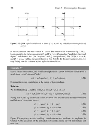
![Sec. 3.3. Digital Modulation 109
Example 3.7 (Continued)
1
2
β
β
cosθ
+ θ
1− sin
,
( )
cosθ θ
sin
,
( )
− 1+
cosθ θ
sin
,
( )
− −1+
cosθ θ
sin
,
( )
+ −1−
Ideal Point
Actual Point
Figure 3.26 Effect of phase mismatch on QPSK constellation.
α1
α2
Baseband
Data
S/P
Converter
A
B t
Binary
A
B
Figure 3.27 Phase transitions in QPSK signal due to simultaneous transitions at A and B.
An important drawback of QPSK stems from the large phase changes at the end of
each symbol. As depicted in Fig. 3.27, when the waveforms at the output of the S/P con-
verter change simultaneously from, say, [21 2 1] to [11 1 1], the carrier experiences
a 1808 phase step, or equivalently, a transition between two diagonally opposite points in
the constellation. To understand why this is a serious issue, first recall from Section 3.3.1
that the baseband pulses are usually shaped so as to tighten the spectrum. What happens if
the symbol pulses at nodes A and B are shaped before multiplication by the carrier phases?
As illustrated in Fig. 3.28, with pulse shaping, the output signal amplitude (“envelope”)
experiences large changes each time the phase makes a 908 or 1808 transition. The resulting](https://image.slidesharecdn.com/rfmicroelectronicsrazavi-230814101614-71259b59/85/RF-MICROELECTRONICS_Razavi-pdf-134-320.jpg)
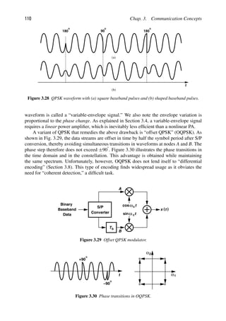
![Sec. 3.3. Digital Modulation 111
A variant of QPSK that can be differentially encoded is “π/4-QPSK” [4, 5]. In this
case, the signal set consists of two QPSK schemes, one rotated 458 with respect to the
other:
x1(t) 5 Ac cos
ωct 1 k
π
4
k odd, (3.38)
x2(t) 5 Ac cos
ωct 1 k
π
4
k even. (3.39)
As shown in Fig. 3.31, the modulation is performed by alternately taking the output from
each QPSK generator.
)
(t
x
Tb
Baseband
Data
A t
cos
c ω
( π
k )
4
c k = 1, 3, 5, 7
A t
cos
c ω
( π
k )
4
c k
2
= 2, 4, 6, 8
Figure 3.31 Conceptual generation of π/4-QPSK signal.
To better understand the operation, let us study the simple π/4-QPSK generator shown
in Fig. 3.32. After S/P conversion, the digital signal levels are scaled and shifted so as
to present ±1 in the upper QPSK modulator and 0 and
√
2 in the lower. The outputs are
therefore equal to x1(t) 5 α1 cos ωct 1 α2 sin ωct, where [α1 α2] 5 [±Ac ± Ac], and
x2(t) 5 β1 cos ωct 1 β2 sin ωct, where [β1 β2] 5 [0 ±
√
2Ac] and [±
√
2Ac 0]. Thus, the
constellation alternates between the two depicted in Fig. 3.32. Now consider a baseband
sequence of [11, 01, 10, 11, 01]. As shown in Fig. 3.33, the first pair, [1 1], is converted to
[1Ac 1 Ac] in the upper arm, producing y(t) 5 Ac cos(ωct 1 π/4). The next pair, [0 1],
is converted to [0 2
√
2Ac] in the lower arm, yielding y(t) 5 2
√
2Ac cos ωct. Following
t
cos
t
sinω c
ωc
S/P
Converter
Baseband
Data
S/P
Converter
+1, −1
+1, −1
0, 2
)
(t
x
Tb
2
Ac
Ac
t
cos
t
sinω c
ωc
Ac
Ac
0, 2
Figure 3.32 Generation of π/4-QPSK signals.](https://image.slidesharecdn.com/rfmicroelectronicsrazavi-230814101614-71259b59/85/RF-MICROELECTRONICS_Razavi-pdf-136-320.jpg)
![112 Chap. 3. Communication Concepts
t
ONE
ZERO
ONE ONE
ZERO
ONE ONE
ONE
ZERO
ONE
(a) (b)
Figure 3.33 (a) Evolution of π/4-QPSK in time domain, (b) possible phase transitions in the
constellation.
the values of y(t) for the entire sequence, we note that the points chosen from the two
constellations appear as in Fig. 3.33(a) as a function of time. The key point here is that,
since no two consecutive points are from the same constellation, the maximum phase step
is 1358, 458 less than that in QPSK. This is illustrated in Fig. 3.33(b). Thus, in terms of the
maximum phase change, π/4-QPSK is an intermediate case between QPSK and OQPSK.
By virtue of baseband pulse shaping, QPSK and its variants provide high spectral effi-
ciency but lead to poor power efficiency because they dictate linear power amplifiers. These
modulation schemes are used in a number of applications (Section 3.7).
3.3.4 GMSK and GFSK Modulation
A class of modulation schemes that does not require linear power amplifiers, thus exhibiting
high power efficiency, is “constant-envelope modulation.” For example, an FSK waveform
expressed as xFSK(t) 5 Ac cos[ωct 1 m
xBB(t)dt] has a constant envelope. To arrive at
variants of FSK, let us first consider the implementation of a frequency modulator. As
illustrated in Fig. 3.34(a), an oscillator whose frequency can be tuned by a voltage [called
a “voltage-controlled oscillator” (VCO)] performs frequency modulation. In FSK, square
baseband pulses are applied to the VCO, producing a broad output spectrum due to the
abrupt changes in the VCO frequency. We therefore surmise that smoother transitions
between ONEs and ZEROs in the baseband signal can tighten the spectrum. A common
method of pulse shaping for frequency modulation employs a “Gaussian filter,” i.e., one
whose impulse response is a Gaussian pulse. Thus, as shown in Fig. 3.34(b), the pulses
applied to the VCO gradually change the output frequency, leading to a narrower spectrum.
Called “Gaussian minimum shift keying” (GMSK), the scheme of Fig. 3.34(b) is used
in GSM cell phones (Section 3.7). The GMSK waveform can be expressed as
xGMSK(t) 5 Ac cos[ωct 1 m
xBB(t) ∗ h(t)dt], (3.40)
where h(t) denotes the impulse response of the Gaussian filter. The modulation index, m,
is a dimensionless quantity and has a value of 0.5. Owing to its constant envelope, GMSK
allows optimization of PAs for high efficiency—with little attention to linearity.](https://image.slidesharecdn.com/rfmicroelectronicsrazavi-230814101614-71259b59/85/RF-MICROELECTRONICS_Razavi-pdf-137-320.jpg)
![Sec. 3.3. Digital Modulation 113
)
(t
xBB
t t
ONE ZERO
)
(t
xFSK
Filter
Gaussian
t
t
)
(t
xGMSK
(a)
(b)
VCO
VCO
)
(t
xBB
t
ONE ZERO
Figure 3.34 Generation of (a) FSK and (b) GMSK signals.
A slightly different version of GMSK, called Gaussian frequency shift keying (GFSK),
is employed in Bluetooth. The GFSK waveform is also given by Eq. (3.40) but with m 5 0.3.
Example 3.8
Construct a GMSK modulator using a quadrature upconverter.
Solution:
Let us rewrite Eq. (3.40) as
xGMSK(t) 5 Ac cos[m
xBB(t) ∗ h(t)dt] cos ωct 2 Ac sin[m
xBB(t) ∗ h(t)dt] sin ωct. (3.41)
We can therefore construct the modulator as shown in Fig. 3.35, where a Gaussian filter
is followed by an integrator and two arms that compute the sine and cosine of the signal
at node A. The complexity of these operations is much more easily afforded in the digital
domain than in the analog domain (Chapter 4).
)
(t
xBB
Filter
Gaussian
( )
( )
cos
( )
sin
t
cos
t
sinω c
ωc
)
(t
xGMSK
Digital Analog
A
Figure 3.35 Mixed-mode generation of GMSK signal.](https://image.slidesharecdn.com/rfmicroelectronicsrazavi-230814101614-71259b59/85/RF-MICROELECTRONICS_Razavi-pdf-138-320.jpg)
![114 Chap. 3. Communication Concepts
3.3.5 Quadrature Amplitude Modulation
Our study of PSK and QPSK has revealed a twofold reduction in the spectrum as a result
of impressing the information on the quadrature components of the carrier. Can we extend
this idea to further tighten the spectrum? A method that accomplishes this goal is called
“quadrature amplitude modulation” (QAM).
To arrive at QAM, let us first draw the four possible waveforms for QPSK corre-
sponding to the four points in the constellation. As predicted by Eq. (3.31) and shown
in Fig. 3.36(a), each quadrature component of the carrier is multipled by 11 or 21 accord-
ing to the values of b2m and b2m11. Now suppose we allow four possible amplitudes for the
sine and cosine waveforms, e.g., ±1 and ±2, thus obtaining 16 possible output waveforms.
Figure 3.36(b) depicts a few examples of such waveforms. In other words, we group four
consecutive bits of the binary baseband stream and select one of the 16 waveforms accord-
ingly. Called “16QAM,”6
the resulting output occupies one-fourth the bandwidth of PSK
and is expressed as
x16QAM(t) 5 α1Ac cos ωct 2 α2Ac sin ωct α1 5 ±1, ±2, α2 5 ±1, ±2. (3.42)
The constellation of 16QAM can be constructed using the 16 possible combinations of
[α1 α2] (Fig. 3.37). For a given transmitted power [e.g., the rms value of the waveforms
shown in Fig. 3.36(b)], the points in this constellation are closer to one another than those
in the QPSK constellation, making the detection more sensitive to noise. This is the price
paid for saving bandwidth.
In addition to a “dense” constellation, 16QAM also exhibits large envelope variations,
as exemplified by the waveforms in Fig. 3.36. Thus, this type of modulation requires a
t
cos
t
sinω c
ωc
+
−
t
cos
t
sinω c
ωc
+
+
t
cos
t
sinω c
ωc
−
t
cos
t
sinω c
ωc
+
− −
t
cos
t
sinω c
ωc
+
+2
t
cos
t
sinω c
ωc
+2
+2
t
cos
t
sinω c
ωc
+2
−
(a)
(b)
Figure 3.36 Amplitude combinations in (a) QPSK and (b) 16QAM.
6. Also known as QAM16.](https://image.slidesharecdn.com/rfmicroelectronicsrazavi-230814101614-71259b59/85/RF-MICROELECTRONICS_Razavi-pdf-139-320.jpg)
![Sec. 3.3. Digital Modulation 115
I
+1 +2
−1
−2
Q
+1
+2
−1
−2
Figure 3.37 Constellation of 16QAM signal.
highly-linear power amplifier. We again observe the trade-offs among bandwidth efficiency,
detectability, and power efficiency.
The concept of QAM can be extended to even denser constellations. For example, if
eight consecutive bits in the binary baseband stream are grouped and, accordingly, each
quadrature component of the carrier is allowed to have eight possible amplitudes, then
64QAM is obtained. The bandwidth is therefore reduced by a factor of eight with respect
to that of PSK, but the detection and power amplifier design become more difficult.
A number of applications employ QAM to save bandwidth. For example,
IEEE802.11g/a uses 64QAM for the highest data rate (54 Mb/s).
3.3.6 Orthogonal Frequency Division Multiplexing
Communication in a wireless environment entails a serious issue called “multipath prop-
agation.” Illustrated in Fig. 3.38(a), this effect arises from the propagation of the electro-
magnetic waves from the transmitter to the receiver through multiple paths. For example,
one wave directly propagates from the TX to the RX while another is reflected from a wall
before reaching the receiver. Since the phase shift associated with reflection(s) depends on
both the path length and the reflecting material, the waves arrive at the RX with vastly
different delays, or a large “delay spread.” Even if these delays do not result in destruc-
tive interference of the rays, they may lead to considerable intersymbol interference. To
understand this point, suppose, for example, two ASK waveforms containing the same
information reach the RX with different delays [Fig. 3.38(b)]. Since the antenna senses the
sum of these waveforms, the baseband data consists of two copies of the signal that are
shifted in time, thus experiencing ISI [Fig. 3.38(c)].
The ISI resulting from multipath effects worsens for larger delay spreads or higher bit
rates. For example, a data rate of 1 Mb/s becomes sensitive to multipath propagation if the
delay spread reaches a fraction of a microsecond. As a rule of thumb, we say communica-
tion inside office buildings and homes begins to suffer from multipath effects for data rates
greater than 10 Mb/s.
How does wireless communication handle higher data rates? An interesting method of
delay spread mitigation is called “orthogonal frequency division multiplexing” (OFDM).
Consider the “single-carrier” modulated spectrum shown in Fig. 3.39(a), which occupies
a relatively large bandwidth due to a high data rate of rb bits per second. In OFDM, the
baseband data is first demultiplexed by a factor of N, producing N streams each having](https://image.slidesharecdn.com/rfmicroelectronicsrazavi-230814101614-71259b59/85/RF-MICROELECTRONICS_Razavi-pdf-140-320.jpg)
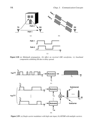
![Sec. 3.3. Digital Modulation 117
a (symbol) rate of rb/N [Fig. 3.39(b)]. The N streams are then impressed on N differ-
ent carrier frequencies, fc1-fcN, leading to a “multi-carrier” spectrum. Note that the total
bandwidth and data rate remain equal to those of the single-carrier spectrum, but the multi-
carrier signal is less sensitive to multipath effects because each carrier contains a low-rate
data stream and can therefore tolerate a larger delay spread.
Each of the N carriers in Fig. 3.39(b) is called a “subcarrier” and each resulting
modulated output a “subchannel.” In practice, all of the subchannels utilize the same mod-
ulation scheme. For example, IEEE802.11a/g employs 48 subchannels with 64QAM in
each for the highest data rate (54 Mb/s). Thus, each subchannel carries a symbol rate of
(54 Mb/s)/48/85141 ksymbol/s.
Example 3.9
It appears that an OFDM transmitter is very complex as it requires tens of carrier fre-
quencies and modulators (i.e., tens of oscillators and mixers). How is OFDM realized in
practice?
Solution:
In practice, the subchannel modulations are performed in the digital baseband and subse-
quently converted to analog form. In other words, rather than generate a1(t) cos[ωct 1
φ1(t)] 1 a2(t) cos[ωct 1 ωt 1 φ2(t)] 1 · · · , we first construct a1(t) cos φ1(t) 1
a2(t) cos[ ωt 1 φ2(t)] 1 · · · and a1(t) sin φ1(t) 1 a2(t) sin[ ωt 1 φ2(t)] 1 · · · . These
components are then applied to a quadrature modulator with an LO frequency of ωc.
While providing greater immunity to multipath propagation, OFDM imposes severe
linearity requirements on power amplifiers. This is because the N (orthogonal) subchannels
summed at the output of the system in Fig. 3.39(b) may add constructively at some point in
time, creating a large amplitude, and destructively at some other point in time, producing a
small amplitude. That is, OFDM exhibits large envelope variations even if the modulated
waveform in each subchannel does not.
In the design of power amplifiers, it is useful to have a quantitative measure of the
signal’s envelope variations. One such measure is the “peak-to-average ratio” (PAR). As
illustrated in Fig. 3.40, PAR is defined as the ratio of the largest value of the square of the
f
f f
c1 cN t
Peak
Amplitude
Amplitude
Average
Figure 3.40 Large amplitude variations due to OFDM.](https://image.slidesharecdn.com/rfmicroelectronicsrazavi-230814101614-71259b59/85/RF-MICROELECTRONICS_Razavi-pdf-142-320.jpg)
![118 Chap. 3. Communication Concepts
signal (voltage or current) divided by the average value of the square of the signal:
PAR 5
Max[x2(t)]
x2(t)
. (3.43)
We note that three effects lead to a large PAR: pulse shaping in the baseband, amplitude
modulation schemes such as QAM, and orthogonal frequency division multiplexing. For N
subcarriers, the PAR of an OFDM waveform is about 2 ln N if N is large [6].
3.4 SPECTRAL REGROWTH
In our study of modulation schemes, we have mentioned that variable-envelope signals
require linear PAs, whereas constant-envelope signals do not. Of course, modulation
schemes such as 16QAM that carry information in their amplitude levels experience corru-
ption if the PA compresses the larger levels, i.e., moves the outer points of the constellation
toward the origin. But even variable-envelope signals that carry no significant information
in their amplitude (e.g., QPSK with baseband pulse-shaping) create an undesirable effect
in nonlinear PAs. Called “spectral regrowth,” this effect corrupts the adjacent channels.
A modulated waveform x(t) 5 A(t) cos[ωct 1 φ(t)] is said to have a constant envelope
if A(t) does not vary with time. Otherwise, we say the signal has a variable envelope.
Constant- and variable-envelope signals behave differently in a nonlinear system. Suppose
A(t) 5 Ac and the system exhibits a third-order memoryless nonlinearity:
y(t) 5 α3x3
(t) 1 · · · (3.44)
5 α3A3
c cos3
[ωct 1 φ(t)] 1 · · · (3.45)
5
α3A3
c
4
cos[3ωct 1 3φ(t)] 1
3α3A3
c
4
cos[ωct 1 φ(t)] (3.46)
The first term in (3.46) represents a modulated signal around ω 5 3ωc. Since the bandwidth
of the original signal, Ac cos[ωct 1 φ(t)], is typically much less than ωc, the bandwidth
occupied by cos[3ωct 1 3φ(t)] is small enough that it does not reach the center frequency
of ωc. Thus, the shape of the spectrum in the vicinity of ωc remains unchanged.
Now consider a variable-envelope signal applied to the above nonlinear system.
Writing x(t) as
x(t) 5 xI(t) cos ωct 2 xQ(t) sin ωct, (3.47)
where xI and xQ(t) are the baseband I and Q components, we have
y(t) 5 α3[xI(t) cos ωct 2 xQ(t) sin ωct]3
1 · · · (3.48)
5 α3x3
I (t)
cos 3ωct 1 3 cos ωct
4
2 α3x3
Q(t)
2cos 3ωct 1 3 sin ωct
4
. (3.49)
Thus, the output contains the spectra of x3
I (t) and x3
Q(t) centered around ωc. Since these
components generally exhibit a broader spectrum than do xI(t) and xQ(t), we say the
spectrum “grows” when a variable-envelope signal passes through a nonlinear system.
Figure 3.41 summarizes our findings.](https://image.slidesharecdn.com/rfmicroelectronicsrazavi-230814101614-71259b59/85/RF-MICROELECTRONICS_Razavi-pdf-143-320.jpg)
![120 Chap. 3. Communication Concepts
f1
f1
f1
f1
f1 f1
f1
f1
f1
f2
f2
(a) (b)
Figure 3.42 (a) Simple cellular system, (b) 7-cell reuse pattern.
[Fig. 3.42(a)]. The idea is that if the center cell uses a frequency f1 for communication,
the 6 neighboring cells cannot utilize this frequency, but the cells beyond the immediate
neighbors may. In practice, more efficient frequency assignment leads to the “7-cell” reuse
pattern shown in Fig. 3.42(b). Note that in reality each cell utilizes a group of frequencies.
The mobile units in each cell of Fig. 3.42(b) are served by a base station, and all of the
base stations are controlled by a “mobile telephone switching office” (MTSO).
Co-Channel Interference An important issue in a cellular system is how much two
cells that use the same frequency interfere with each other (Fig. 3.43). Called “co-channel
interference” (CCI), this effect depends on the ratio of the distance between two co-channel
cells to the cell radius and is independent of the transmitted power. Given by the frequency
reuse plan, this ratio is approximately equal to 4.6 for the 7-cell pattern of Fig. 3.42(b) [7].
It can be shown that this value yields a signal-to-co-channel interference ratio of 18 dB [7].
f1
f1
f1 f1
f1
Figure 3.43 Co-channel interference.
Hand-off What happens when a mobile unit “roams” from cell A to cell B
(Fig. 3.44)? Since the power level received from the base station in cell A is insufficient
MTSO
Cell A
Cell B
Figure 3.44 Problem of hand-off.](https://image.slidesharecdn.com/rfmicroelectronicsrazavi-230814101614-71259b59/85/RF-MICROELECTRONICS_Razavi-pdf-145-320.jpg)
![Sec. 3.5. Mobile RF Communications 121
to maintain communication, the mobile must change its server to the base station in cell
B. Furthermore, since adjacent cells do not use the same group of frequencies, the channel
must also change. Called “hand-off,” this process is performed by the MTSO. Once the
level received by the base station in cell A drops below a threshold, the MTSO hands off
the mobile to the base station in cell B, hoping that the latter is close enough. This strategy
fails with relatively high probability, resulting in dropped calls.
To improve the hand-off process, second-generation cellular systems allow the mobile
unit to measure the received signal level from different base stations, thus performing hand-
off when the path to the second base station has sufficiently low loss [7].
Path Loss and Multipath Fading Propagation of signals in a mobile communication
environment is quite complex. We briefly describe some of the important concepts here.
Signals propagating through free space experience a power loss proportional to the square
of the distance, d, from the source. In reality, however, the signal travels through both a
direct path and an indirect, reflective path (Fig. 3.45). It can be shown that in this case, the
loss increases with the fourth power of the distance [7]. In crowded areas, the actual loss
profile may be proportional to d2 for some distance and d4 for another.
Direct Path
Reflective Path
4
1
d
Loss
(log scale)
Figure 3.45 Indirect signal propagation and resulting loss profile.
In addition to the overall loss profile depicted in Fig. 3.45, another mechanism gives
rise to fluctuations in the received signal level as a function of distance. Since the two
signals shown in Fig. 3.45 generally experience different phase shifts, possibly arriving at
the receiver with opposite phases and roughly equal amplitudes, the net received signal
may be very small. Called “multipath fading” and illustrated in Fig. 3.46, this phenomenon
introduces enormous variations in the signal level as the receiver moves by a fraction of
the wavelength. Note that multipath propagation creates fading and/or ISI.
d
Loss
(log scale)
Figure 3.46 Multipath loss profile.](https://image.slidesharecdn.com/rfmicroelectronicsrazavi-230814101614-71259b59/85/RF-MICROELECTRONICS_Razavi-pdf-146-320.jpg)
![122 Chap. 3. Communication Concepts
In reality, since the transmitted signal is reflected by many buildings and moving
cars, the fluctuations are quite irregular. Nonetheless, the overall received signal can be
expressed as
xR(t) 5 a1(t) cos(ωct 1 θ1) 1 a2(t) cos(ωct 1 θ2) 1 · · · 1 an cos(ωct 1 θn) (3.50)
5
⎡
⎣
n
j51
aj(t) cos θj
⎤
⎦ cos ωct 2
⎡
⎣
n
j51
aj(t) sin θj
⎤
⎦ sin ωct. (3.51)
For large n, each summation has a Gaussian distribution. Denoting the first summation by
A and the second by B, we have
xR(t) 5
A2 1 B2 cos(ωct 1 φ), (3.52)
where φ 5 tan21(B/A). It can be shown that the amplitude, Am 5
√
A2 1 B2, has a
Rayleigh distribution (Fig. 3.47) [1], exhibiting losses greater than 10 dB below the mean
for approximately 6% of the time.
x
)
(
Px x
Figure 3.47 Rayleigh distribution.
From the above discussion, we conclude that in an RF system the transmitter out-
put power and the receiver dynamic range must be chosen so as to accommodate signal
level variations due to both the overall path loss (roughly proportional to d4) and the deep
multipath fading effects. While it is theoretically possible that multipath fading yields a
zero amplitude (infinite loss) at a given distance, the probability of this event is negligible
because moving objects in a mobile environment tend to “soften” the fading.
Diversity The effect of fading can be lowered by adding redundancy to the transmis-
sion or reception of the signal. “Space diversity” or “antenna diversity” employs two or
more antennas spaced apart by a significant fraction of the wavelength so as to achieve a
higher probability of receiving a nonfaded signal.
“Frequency diversity” refers to the case where multiple carrier frequencies are used,
with the idea that fading is unlikely to occur simultaneously at two frequencies sufficiently
far from each other. “Time diversity” is another technique whereby the data is transmitted
or received more than once to overcome short-term fading.
Delay Spread Suppose two signals in a multipath environment experience roughly
equal attenuations but different delays. This is possible because the absorption coeffi-
cient and phase shift of reflective or refractive materials vary widely, making it likely for
two paths to exhibit equal loss and unequal delays. Addition of two such signals yields
x(t) 5 A cos ω(t2τ1)1A cos ω(t2τ2) 5 2A cos[(2ωt2ωτ1 2ωτ2)/2] cos[ω(τ1 2τ2)/2],
where the second cosine factor relates the fading to the “delay spread,” τ 5 τ1 2 τ2. An](https://image.slidesharecdn.com/rfmicroelectronicsrazavi-230814101614-71259b59/85/RF-MICROELECTRONICS_Razavi-pdf-147-320.jpg)
![Sec. 3.6. Multiple Access Techniques 123
ω
Channel
ω
Channel
Δτ
1
Δτ
1
cos
ω Δτ
2
cos
ω Δτ
2
(a) (b)
Figure 3.48 (a) Flat and (b) frequency-selective fading.
important issue here is the frequency dependence of the fade. As illustrated in Fig. 3.48,
small delay spreads yield a relatively flat fade, whereas large delay spreads introduce
considerable variation in the spectrum.
In a multipath environment, many signals arrive at the receiver with different delays,
yielding rms delay spreads as large as several microseconds and hence fading bandwidths
of several hundreds of kilohertz. Thus, an entire communication channel may be suppressed
during such a fade.
Interleaving The nature of multipath fading and the signal processing techniques
used to alleviate this issue is such that errors occur in clusters of bits. In order to lower the
effect of these errors, the baseband bit stream in the transmitter undergoes “interleaving”
before modulation. An interleaver in essence scrambles the time order of the bits according
to an algorithm known by the receiver [7].
3.6 MULTIPLE ACCESS TECHNIQUES
3.6.1 Time and Frequency Division Duplexing
The simplest case of multiple access is the problem of two-way communication by a
transceiver, a function called “duplexing.” In old walkie-talkies, for example, the user
would press the “talk” button to transmit while disabling the receive path and release the
button to listen while disabling the transmit path. This can be considered a simple form of
“time division duplexing,” (TDD), whereby the same frequency band is utilized for both
transmit (TX) and receive (RX) paths but the system transmits for half of the time and
receives for the other half. Illustrated in Fig. 3.49, TDD is usually performed fast enough
to be transparent to the user.
Another approach to duplexing is to employ two different frequency bands for the
transmit and receive paths. Called “frequency-division duplexing” (FDD) and shown in
Fig. 3.50, this technique incorporates band-pass filters to isolate the two paths, allowing
simultaneous transmission and reception. Since two such transceivers cannot communicate
directly, the TX band must be translated to the RX band at some point. In wireless networks,
this translation is performed in the base station.
It is instructive to contrast the two duplexing methods by considering their merits and
drawbacks. In TDD, an RF switch with a loss less than 1 dB follows the antenna to alter-
nately enable and disable the TX and RX paths. Even though the transmitter output power](https://image.slidesharecdn.com/rfmicroelectronicsrazavi-230814101614-71259b59/85/RF-MICROELECTRONICS_Razavi-pdf-148-320.jpg)
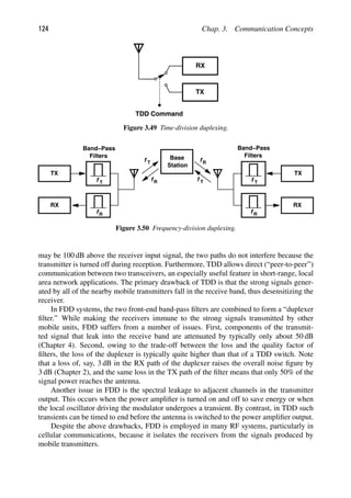
![126 Chap. 3. Communication Concepts
Transceiver 1
Enable
Transceiver
Enable
2
Transceiver
Enable
N
t
t
t
Tsl
TF
Figure 3.52 Time-division multiple access.
of users can be accommodated in each frame. Third, even with FDD, the TDMA bursts
can be timed such that the receive and transmit paths in each transceiver are never enabled
simultaneously.
The need for A/D conversion, digital modulation, time slot and frame synchronization,
etc., makes TDMA more complex than FDMA. With the advent of VLSI DSPs, however,
this drawback is no longer a determining factor. In most actual TDMA systems, a combi-
nation of TDMA and FDMA is utilized. In other words, each of the channels depicted in
Fig. 3.51 is time-shared among many users.
3.6.4 Code-Division Multiple Access
Our discussion of FDMA and TDMA implies that the transmitted signals in these systems
avoid interfering with each other in either the frequency domain or the time domain. In
essence, the signals are orthogonal in one of these domains. A third method of multiple
access allows complete overlap of signals in both frequency and time, but employs “ortho-
gonal messages” to avoid interference. This can be understood with the aid of an analogy [8].
Suppose many conversations are going on in a crowded party. To minimize crosstalk, dif-
ferent groups of people can be required to speak in different pitches(!) (FDMA), or only one
group can be allowed to converse at a time (TDMA). Alternatively, each group can be asked
to speak in a different language. If the languages are orthogonal (at least in nearby groups)
and the voice levels are roughly the same, then each listener can “tune in” to the proper
language and receive information while all groups talk simultaneously.
Direct-Sequence CDMA In “code-division multiple access,” different languages
are created by means of orthogonal digital codes. At the beginning of communication,
a certain code is assigned to each transmitter-receiver pair, and each bit of the baseband
data is “translated” to that code before modulation. Shown in Fig. 3.53(a) is an example
where each baseband pulse is replaced with an 8-bit code by multiplication. A method of](https://image.slidesharecdn.com/rfmicroelectronicsrazavi-230814101614-71259b59/85/RF-MICROELECTRONICS_Razavi-pdf-151-320.jpg)
![Sec. 3.6. Multiple Access Techniques 127
t
t
t
(a) (b)
t
Baseband
Pulse
Figure 3.53 (a) Encoding operation in DS-CDMA, (b) examples of Walsh code.
generating orthogonal codes is based on Walsh’s recursive equation:
W1 5 0 (3.53)
W2n 5
Wn Wn
Wn Wn
(3.54)
where Wn is derived from Wn by replacing all the entries with their complements. For
example,
W2 5
0 0
0 1
(3.55)
Fig. 3.53(b) shows examples of 8-bit Walsh codes (i.e., each row of W8).
In the receiver, the demodulated signal is decoded by multiplying it by the same
Walsh code. In other words, the receiver correlates the signal with the code to recover
the baseband data.
How is the received data affected when another CDMA signal is present? Suppose
two CDMA signals x1(t) and x2(t) are received in the same frequency band. Writing the
signals as xBB1(t) · W1(t) and xBB2(t) · W2(t), where W1(t) and W2(t) are Walsh functions,
we express the output of the demodulator as y(t) 5 [xBB1(t).W1(t) 1 xBB2(t).W2(t)].W1(t).
Thus, if W1(t) and W2(t) are exactly orthogonal, then y(t) 5 xBB1(t) · W1(t). In reality,
however, x1(t) and x2(t) may experience different delays, leading to corruption of y(t) by
xBB2(t). Nevertheless, for long codes the result appears as random noise.
The encoding operation of Fig. 3.53(a) increases the bandwidth of the data spectrum
by the number of pulses in the code. This may appear in contradiction to our emphasis thus
far on spectral efficiency. However, since CDMA allows the widened spectra of many users
to fall in the same frequency band (Fig. 3.54), this access technique has no less capacity
than do FDMA and TDMA. In fact, CDMA can potentially achieve a higher capacity than
the other two [9].
CDMA is a special case of “spread spectrum” (SS) communications, whereby the base-
band data of each user is spread over the entire available bandwidth. In this context, CDMA
is also called “direct sequence” SS (DS-SS) communication, and the code is called the
“spreading sequence” or “pseudo-random noise.” To avoid confusion with the baseband
data, each pulse in the spreading sequence is called a “chip” and the rate of the sequence](https://image.slidesharecdn.com/rfmicroelectronicsrazavi-230814101614-71259b59/85/RF-MICROELECTRONICS_Razavi-pdf-152-320.jpg)
![128 Chap. 3. Communication Concepts
t
ω
ω ωc
t
ω
ω ωc
User 1
User 2
Figure 3.54 Overlapping spectra in CDMA.
is called the “chip rate.” Thus, the spectrum is spread by the ratio of the chip rate to the
baseband bit rate.
It is instructive to reexamine the above RX decoding operation from a spread spectrum
point of view (Fig. 3.55). Upon multiplication by W1(t), the desired signal is “despread,”
with its bandwidth returning to the original value. The unwanted signal, on the other hand,
remains spread even after multiplication because of its low correlation with W1(t). For
a large number of users, the spread spectra of unwanted signals can be viewed as white
Gaussian noise.
ω
)
(t
W1
ω
ω
Signal 1
Signal 2
Signal 1
Signal 2
Figure 3.55 Despreading operation in a CDMA receiver.
An important feature of CDMA is its soft capacity limit [7]. While in FDMA and
TDMA the maximum number of users is fixed once the channel width or the time slots are
defined, in CDMA increasing the number of users only gradually (linearly) raises the noise
floor [7].
A critical issue in DS-CDMA is power control. Suppose, as illustrated in Fig. 3.56,
the desired signal power received at a point is much lower than that of an unwanted trans-
mitter,7
for example because the latter is at a shorter distance. Even after despreading,
the strong interferer greatly raises the noise floor, degrading the reception of the desired
signal. For multiple users, this means that one high-power transmitter can virtually halt
7. This situation arises in our party analogy if two people speak much more loudly than others. Even with
different languages, communication becomes difficult.](https://image.slidesharecdn.com/rfmicroelectronicsrazavi-230814101614-71259b59/85/RF-MICROELECTRONICS_Razavi-pdf-153-320.jpg)
![Sec. 3.7. Wireless Standards 131
quality, the EVM is specified. Second, to guarantee that the TX out-of-channel
emissions remain sufficiently small, a TX “spectral mask” is defined. As explained
in Section 3.4, excessive PA nonlinearity may violate this mask. Also, the stan-
dard poses a limit on other unwanted transmitted components, e.g., spurs and
harmonics.
7. RX Sensitivity. The standard specifies the acceptable receiver sensitivity, usually
in terms of a maximum bit error rate, BERmax. In some cases, the sensitivity is
commensurate with the data rate, i.e., a higher sensitivity is stipulated for lower
data rates.
8. RX Input Level Range. The desired signal sensed by a receiver may range from
the sensitivity level to a much larger value if the RX is close to the TX. Thus,
the standard specifies the desired signal range that the receiver must handle with
acceptable noise or distortion.
9. RX Tolerance to Blockers. The standard specifies the largest interferer that the RX
must tolerate while receiving a small desired signal. This performance is typically
defined as illustrated in Fig. 3.58. In the first step, a modulated signal is applied at
the “reference” sensitivity level and the BER is measured to remain below BERmax
[Fig. 3.58(a)]. In the second step, the signal level is raised by 3 dB and a blocker
is added to the input and its level is gradually raised. When the blocker reaches the
specified level, the BER must not exceed BERmax [Fig. 3.58(b)]. This test reveals
the compression behavior and phase noise of the receiver. The latter is described in
Chapter 8.
Many standards also stipulate an intermodulation test. For example, as shown
in Fig. 3.59, two blockers (one modulated and another not) are applied along with
the desired signal at 3 dB above the sensitivity level. The receiver BER must not
exceed BERmax as the level of the two blockers reaches the specified level.
In this section, we study a number of wireless standards. In the case of cellular
standards, we focus on the “mobile station” (the handset).
f
Reference
Sensitivity
Receiver
t
BER max
f
Reference
Sensitivity
Receiver
t
BER max
3 dB
Blocker
(a)
(b)
Figure 3.58 Test of a receiver with (a) desired signal at reference sensitivity and (b) desired signal
3 dB above reference sensitivity along with a blocker.](https://image.slidesharecdn.com/rfmicroelectronicsrazavi-230814101614-71259b59/85/RF-MICROELECTRONICS_Razavi-pdf-156-320.jpg)
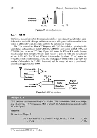
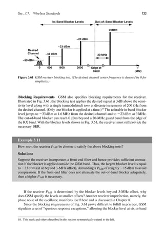
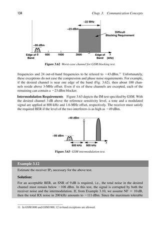
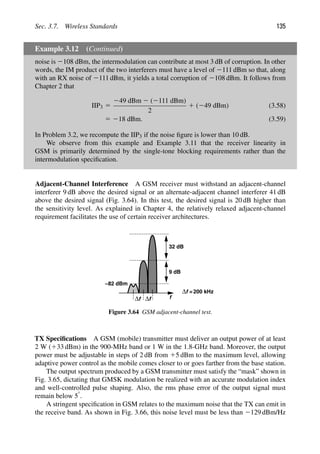
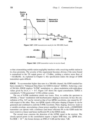
![Sec. 3.7. Wireless Standards 137
Q
I
Figure 3.67 Constellation of 8-PSK (used in EDGE).
3.7.2 IS-95 CDMA
A wireless standard based on direct-sequence CMDA has been proposed by Qualcomm,
Inc., and adopted for North America as IS-95. Using FDD, the air interface employs the
transmit and receive bands shown in Fig. 3.68. In the mobile unit, the 9.6 kb/s baseband data
is spread to 1.23 MHz and subsequently modulated using OQPSK. The link from the base
station to the mobile unit, on the other hand, incorporates QPSK modulation. The logic
is that the mobile must use a power-efficient modulation scheme (Chapter 3), whereas
the base station transmits many channels simultaneously and must therefore employ a
linear power amplifier regardless of the type of modulation. In both directions, IS-95
requires coherent detection, a task accomplished by transmitting a relatively strong “pilot
tone” (e.g., unmodulated carrier) at the beginning of communication to establish phase
synchronization.
In contrast to the other standards studied above, IS-95 is substantially more complex,
incorporating many techniques to increase the capacity while maintaining a reasonable
signal quality. We briefly describe some of the features here. For more details, the reader is
referred to [8, 10, 11].
Duplexer
FDD
f
Modulator
824−849 MHz
869−894 MHz
Digital
Baseband
Signal
1.23 MHz
OQPSK
PN Sequence
(9.6 kb/s)
1850−1910 MHz
1930−1980 MHz
Figure 3.68 IS-95 air interface.](https://image.slidesharecdn.com/rfmicroelectronicsrazavi-230814101614-71259b59/85/RF-MICROELECTRONICS_Razavi-pdf-162-320.jpg)
![138 Chap. 3. Communication Concepts
Power Control As mentioned in Section 3.6.4, in CDMA the power levels received
by the base station from various mobile units must differ by no more than approximately
1 dB. In IS-95, the output power of each mobile is controlled by an open-loop procedure
at the beginning of communication so as to perform a rough but fast adjustment. Subse-
quently, the power is set more accurately by a closed-loop method. For open-loop control,
the mobile measures the signal power it receives from the base station and adjusts its
transmitted power so that the sum of the two (in dB) is approximately 273 dBm. If the
receive and transmit paths entail roughly equal attenuation, k dB, and the power transmit-
ted by the base station is Pbs, then the mobile output power Pm satisfies the following:
Pbs 2k1Pm 5 273 dBm. Since the power received by the base station is Pm 2k, we have
Pm 2 k 5 273 dBm 2Pbs, a well-defined value because Pbs is usually fixed. The mobile
output power can be varied by approximately 85 dB in a few microseconds.
Closed-loop power control is also necessary because the above assumption of equal
loss in the transmit and receive paths is merely an approximation. In reality, the two paths
may experience different fading because they operate in different frequency bands. To this
end, the base station measures the power level received from the mobile unit and sends
a feedback signal requesting power adjustment. This command is transmitted once every
1.25 ms to ensure timely adjustment in the presence of rapid fading.
Frequency and Time Diversity Recall from Section 3.5 that multipath fading is
often frequency-selective, causing a notch in the channel transfer function that can be sev-
eral kilohertz wide. Since IS-95 spreads the spectrum to 1.23 MHz, it provides frequency
diversity, exhibiting only 25% loss of the band for typical delay spreads [8].
IS-95 also employs time diversity to use multipath signals to advantage. This is accom-
plished by performing correlation on delayed replicas of the received signal (Fig. 3.69).
Called a “rake receiver,” such a system combines the delayed replicas with proper weight-
ing factors, αj, to obtain the maximum signal-to-noise ratio at the output. That is, if the
output of one correlator is corrupted, then the corresponding weighting factor is reduced
and vice versa.
Rake receivers are a unique feature of CDMA. Since the chip rate is much higher than
the fading bandwidth, and since the spreading codes are designed to have negligible corre-
lation for delays greater than a chip period, multipath effects do not introduce intersymbol
interference. Thus, each correlator can be synchronized to one of the multipath signals.
Δ Δ Δ
α1 α α α
2 3 4
)
(t
x
)
(t
y
Figure 3.69 Rake receiver.](https://image.slidesharecdn.com/rfmicroelectronicsrazavi-230814101614-71259b59/85/RF-MICROELECTRONICS_Razavi-pdf-163-320.jpg)
![140 Chap. 3. Communication Concepts
f
f
Δ f
Δ
f
Δ
Transmitted
Channel
= 5 MHz
f
0
Relative
Power
(dB)
2.5 3.5 7.5 8.5 12.5
0
−33.5
−49
−53
−63
(MHz)
(a) (b)
33 dB
43 dB
Figure 3.71 Transmitter (a) adjacent-channel power test, and (b) emission mask in IMT-2000.
IMT-2000 stipulates two sets of specifications to quantify the limits on the out-of-channel
emissions: (1) the adjacent and alternate adjacent channel powers must be 33 dB and 43 dB
below the main channel, respectively [Fig. 3.71(a)]; (2) the emissions measured in a 30-kHz
bandwidth must satisfy the TX mask shown in Fig. 3.71(b).
The transmitter must also coexist harmoniously with the GSM and DCS1800 stan-
dards. That is, the TX power must remain below 279 dBm in a 100-kHz bandwidth in the
GSM RX band (935 MHz-960 MHz) and below 271 dBm in a 100-kHz bandwidth in the
DCS1800 RX band (1805 MHz-1880 MHz).
Receiver Requirements The receiver reference sensitivity is 2107 dBm. As with GSM,
IMT-2000 receivers must withstand a sinusoidal blocker whose amplitude becomes larger
at greater frequency offsets. Unlike GSM, however, IMT-2000 requires the sinusoidal test
for only out-of-band blocking [Fig. 3.72(a)]. The P1dB necessary here is more relaxed than
that in GSM; e.g., at 85 MHz outside the band, the RX must tolerate a tone of 215 dBm.13
For in-band blocking, IMT-2000 provides the two tests shown in Fig. 3.72(b). Here, the
blocker is modulated such that it behaves as another WCDMA channel, thus causing both
compression and cross modulation.
Example 3.13
Estimate the required P1dB of a WCDMA receiver satisfying the in-band test of Fig. 3.72(b).
Solution:
To avoid compression, P1dB must be 4 to 5 dB higher than the blocker level, i.e.,
P1dB ≈ 240 dBm. To quantify the corruption due to cross modulation, we return to our
derivation in Chapter 2. For a sinusoid A1 cos ω1t and an amplitude-modulated blocker
13. However, if the TX leakage is large, the RX linearity must be quite higher.](https://image.slidesharecdn.com/rfmicroelectronicsrazavi-230814101614-71259b59/85/RF-MICROELECTRONICS_Razavi-pdf-165-320.jpg)

![Sec. 3.7. Wireless Standards 143
f
f
Δ
f
Δ
−93 dBm
−52 dBm
=5 MHz
Figure 3.74 IMT-2000 receiver adjacent-channel test.
3.7.4 Bluetooth
The Bluetooth standard was originally conceived as a low-cost solution for short-range,
moderate-rate data communication. In fact, it was envisioned that the transceiver would
perform modulation and demodulation in the analog domain, requiring little digital signal
processing. In practice, however, some attributes of the standard have made the analog
implementations difficult, calling for substantial processing in the digital domain. Despite
these challenges, Bluetooth has found its place in the consumer market, serving in such
short-reach applications as wireless headsets, wireless keyboards, etc.
Figure 3.75 shows the Bluetooth air interface, indicating operation in the 2.4-GHz ISM
band. Each channel carries 1 Mb/s, occupies 1 MHz, and has a carrier frequency equal to
(2402 1 k) MHz, for k 5 0, · · · , 78. To comply with out-of-band emission requirements
of various countries, the first 2 MHz and last 3.5 MHz of the ISM band are saved as “guard
bands” and not used.
f
Modulator
Digital
Baseband
Signal
1 MHz
(1 Mb/s)
GFSK
TDD
TDD
2.400−2.4835 GHz
2.400−2.4835 GHz
Figure 3.75 Bluetooth air interface.
Transmitter Characteristics The 1-Mb/s baseband data is applied to a Gaussian Fre-
quency Shift Keying (GFSK) modulator. GFSK can be viewed as GMSK with a modulation
index of 0.28 to 0.35. As explained in Section 3.3.4, GMSK modulation can be realized by
a Gaussian filter and a VCO (Fig. 3.76).
The output can be expressed as
xTX(t) 5 A cos[ωct 1 m
xBB(t) ∗ h(t)dt], (3.66)](https://image.slidesharecdn.com/rfmicroelectronicsrazavi-230814101614-71259b59/85/RF-MICROELECTRONICS_Razavi-pdf-168-320.jpg)
![144 Chap. 3. Communication Concepts
Filter
Gaussian
t
)
(t
x
VCO
)
(t
xBB
t
ONE ZERO
GFSK
Figure 3.76 GFSK modulation using a VCO.
t
)
(t
xGFSK
t
fc
f
Δ = 115 kHz
Frequency
Deviation
Figure 3.77 Frequency deviation in Bluetooth.
where h(t) denotes the impulse response of the Gaussian filter. As shown in Fig. 3.77,
Bluetooth specifies a minimum frequency deviation of 115 kHz in the carrier. The peak
frequency deviation, f, is obtained as the maximum difference between the instantaneous
frequency, finst, and the carrier frequency. Differentiating the argument of the cosine in
(3.66) yields finst as
finst 5
1
2π
[ωc 1 mxBB(t) ∗ h(t)], (3.67)
suggesting that
f 5
1
2π
m[xBB(t) ∗ h(t)]max. (3.68)
Since the peak voltage swing at the output of the Gaussian filter is approximately equal to
that of xBB(t),
m
2π
xBB,max 5 115 kHz. (3.69)
As explained in Chapter 8, m is a property of the voltage-controlled oscillator (called the
“gain” of the VCO) and must be chosen to satisfy (3.69).
Bluetooth specifies an output level of 0 dBm (1 mW).14
Along with the constant-
envelope modulation, this relaxed value greatly simplifies the design of the power amplifier,
allowing it to be a simple 50- buffer.
The Bluetooth transmit spectrum mask is shown in Fig. 3.78. At an offset of 550 kHz
from the center of the desired channel, the power measured in a 100-kHz bandwidth must
be at least 20 dB below the TX power measured in the same bandwidth but in the center
14. This corresponds to the most common case of “power class 3.” Other power classes with higher output
levels have also been specified.](https://image.slidesharecdn.com/rfmicroelectronicsrazavi-230814101614-71259b59/85/RF-MICROELECTRONICS_Razavi-pdf-169-320.jpg)
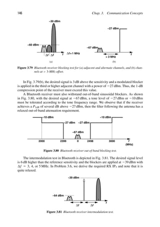
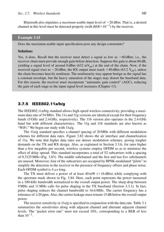
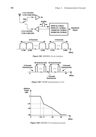
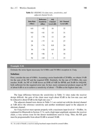
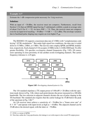
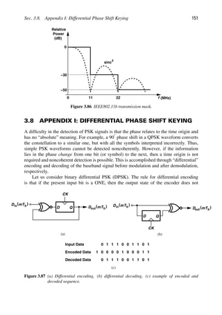
![152 Chap. 3. Communication Concepts
change, and vice versa. This requires an extra starting bit (of arbitrary value). The con-
cept can be better understood by considering the implementation depicted in Fig. 3.87(a).
An exclusive-NOR (XNOR) gate compares the present output bit, Dout(mTb), with the
present input bit, Din(mTb), to determine the next output state:
Dout[(m 1 1)Tb] 5 Din(mTb) ⊕ Dout(mTb), (3.70)
implying that if Din(mTb) 5 1, then Dout[(m 1 1)Tb] 5 Dout(mTb), and if Din(mTb) 5 0
then Dout[(m 1 1)Tb] 5 Dout(mTb). The extra starting bit mentioned above corresponds to
the state of the flipflop before the data sequence begins.
REFERENCES
[1] L. W. Couch, Digital and Analog Communication Systems, Fourth Edition, New York:
Macmillan Co., 1993.
[2] H. E. Rowe, Signals and Noise in Communication Systems, New Jersey: Van Nostrand Co.,
1965.
[3] R. E. Ziemer and R. L. Peterson, Digital Communication and Spread Spectrum Systems, New
York: Macmillan, 1985.
[4] P. A. Baker, “Phase-Modulated Data Sets for Serial Transmission at 2000 and 2400 Bits per
Second,” Part I, AIEE Trans. Communication Electronics, pp. 166–171, July 1962.
[5] Y. Akaiwa and Y. Nagata, “Highly Efficient Digital Mobile Communication with a Linear
Modulation Method,” IEEE J. of Selected Areas in Commnunications, vol. 5, pp. 890–895,
June 1987.
[6] N. Dinur and D. Wulich, “Peak-to-average power ratio in high-order OFDM,” IEEE Tran.
Comm., vol. 49, pp. 1063–1072, June 2001.
[7] T. S. Rappaport, Wireless Communications, Principles and Practice, New Jersey: Prentice
Hall, 1996.
[8] D. P. Whipple, “North American Cellular CDMA,” Hewlett-Packard Journal, pp. 90–97, Dec.
1993.
[9] A. Salmasi and K. S. Gilhousen, “On the System Design Aspects of Code Division Multiple
Access (CDMA) Applied to Digital Cellular and Personal Communications Networks,” Proc.
IEEE Veh. Tech. Conf., pp. 57–62, May 1991.
[10] R. Kerr et al., “The CDMA Digitial Cellular System, An ASIC Overview,” Proceedings of
IEEE CICC, pp. 10.1.1–10.1.7, May 1992.
[11] J. Hinderling et al., “CDMA Mobile Station Modem ASIC,” Proceedings of IEEE CICC,
pp. 10.2.1–10.2.5, May 1992.
PROBLEMS
3.1. Due to imperfections, a 16QAM generator produces α1Ac cos(ωct1 θ)2α2Ac(11)
sin ωct, where α1 5 ±1, ±2 and α2 5 ±1, ±2.
(a) Construct the signal constellation for θ 5 0 but 5 0.
(b) Construct the signal constellation for θ 5 0 but 5 0.
3.2. Repeat Example 3.12 if the noise figure is less than 10 dB.
3.3. Repeat Example 3.12 for WCDMA.](https://image.slidesharecdn.com/rfmicroelectronicsrazavi-230814101614-71259b59/85/RF-MICROELECTRONICS_Razavi-pdf-177-320.jpg)
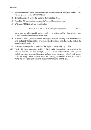

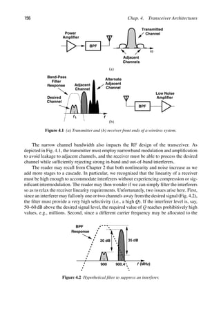
![160 Chap. 4. Transceiver Architectures
Example 4.2 (Continued)
LNA
PA
Duplexer
f
f
BPF
f
TX Leakage
BPF
Frequency Response
Figure 4.6 Use of BPF after LNA to suppress TX leakage.
4.2 RECEIVER ARCHITECTURES
4.2.1 Basic Heterodyne Receivers
As mentioned above, channel-selection filtering proves very difficult at high carrier fre-
quencies. We must devise a method of “translating” the desired channel to a much lower
center frequency so as to permit channel-selection filtering with a reasonable Q. Illustrated
in Fig. 4.7(a), the translation is performed by means of a “mixer,” which in this chapter is
viewed as a simple analog multiplier. To lower the center frequency, the signal is multiplied
by a sinusoid A0 cos ωLOt, which is generated by a local oscillator (LO). Since multiplica-
tion in the time domain corresponds to convolution in the frequency domain, we observe
from Fig. 4.7(b) that the impulses at ±ωLO shift the desired channel to ±(ωin ± ωLO). The
components at ±(ωin 1 ωLO) are not of interest and are removed by the low-pass filter
(LPF) in Fig. 4.7(a), leaving the signal at a center frequency of ωin 2 ωLO. This operation
is called “downconversion mixing” or simply “downconversion.” Due to its high noise, the
downconversion mixer is preceded by a low-noise amplifier [Fig. 4.7(c)].
Called the intermediate frequency (IF), the center of the downconverted channel,
ωin 2 ωLO, plays a critical role in the performance. “Heterodyne” receivers employ an LO
frequency unequal to ωin and hence a nonzero IF.4
How does a heterodyne receiver cover a given frequency band? For an N-channel band,
we can envision two possibilities. (1) The LO frequency is constant and each RF channel
4. In this book, we do not distinguish between heterodyne and “super heterodyne” architectures. The term
heterodyne derives from hetero (different) and dyne (to mix).](https://image.slidesharecdn.com/rfmicroelectronicsrazavi-230814101614-71259b59/85/RF-MICROELECTRONICS_Razavi-pdf-185-320.jpg)
![Sec. 4.2. Receiver Architectures 161
Local
RF
Input
ω
ωin
A cos ωLOt
Oscillator
LPF
IF
Output
in
+
ωin
− ω ω
+
ω
− ω
LO ω
LO
0
0
in
ω ωLO ω
0 in
+ ω ω
− LO in
+ ω ωLO
+
in
ω ωLO
+
− − −
Local
RF
Input
Oscillator
LPF
IF
Output
LNA
(c)
(a)
(b)
Mixer
0
Figure 4.7 (a) Downconversion by mixing, (b) resulting spectra, (c) use of LNA to reduce noise.
is downconverted to a different IF channel [Fig. 4.8(a)], i.e., fIFj 5 fRFj 2 fLO. (2) The LO
frequency is variable so that all RF channels within the band of interest are translated to a
single value of IF [Fig. 4.8(b)], i.e., fLOj 5 fRFj 2 fIF. The latter case is more common as
it simplifies the design of the IF path; e.g., it does not require a filter with a variable center
frequency to select the IF channel of interest and reject the others. However, this approach
demands a feedback loop that precisely defines the LO frequency steps, i.e., a “frequency
synthesizer” (Chapters 9–11).
Problem of Image Heterodyne receivers suffer from an effect called the “image.”
To understand this phenomenon, let us assume a sinusoidal input and express the IF
component as
A cos ωIFt 5 A cos(ωin 2 ωLO)t (4.4)
5 A cos(ωLO 2 ωin)t. (4.5)
That is, whether ωin2ωLO is positive or negative, it yields the same intermediate frequency.
Thus, whether ωin lies above ωLO or below ωLO, it is translated to the same IF. Figure 4.9](https://image.slidesharecdn.com/rfmicroelectronicsrazavi-230814101614-71259b59/85/RF-MICROELECTRONICS_Razavi-pdf-186-320.jpg)
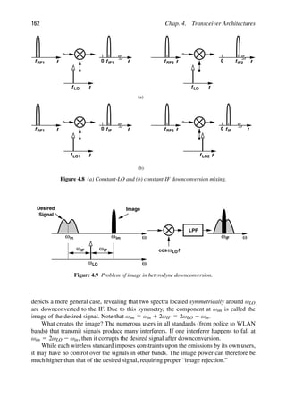
![164 Chap. 4. Transceiver Architectures
Example 4.3 (Continued)
the components at 2ω1 and 2ω2 to the right. Since ωLO ω1, the positive input fre-
quencies remain positive after downconversion, and the negative input frequencies remain
negative.
Now consider the case depicted in Fig. 4.10(b), where ωLO is slightly greater than
ω1. Here, after downconversion the channel at 1ω1 slides to negative frequencies while
that at 1ω2 remains positive. If ωLO reaches (ω1 1 ω2)/2, then the received channels are
translated such that they completely overlap each other at the IF output [Fig. 4.10(c)]. That
is, ω1 and ω2 are images of each other. Finally, if ωLO is greater than ω2, both positive input
frequencies are shifted to negative values, and both negative input frequencies are shifted
to positive values [Fig. 4.10(d)].
Example 4.4
Formulate the downconversion shown in Fig. 4.9 using expressions for the desired signal
and the image.
Solution:
The two components contain modulation, assuming the forms Ain(t) cos[ωint 1 φin(t)] and
Aim(t) cos[ωimt 1 φim(t)], where ωim 5 2ωLO 2 ωin. Upon multiplication by ALO cos ωLOt,
they yield
xIF(t) 5
1
2
Ain(t)ALO cos[(ωin 1 ωLO)t 1 φin(t)] 2
1
2
Ain(t)ALO[cos(ωin 2 ωLO)t 1 φint]
1
1
2
Aim(t)ALO cos[(ωim 1 ωLO)t 1 φim(t)]
2
1
2
Aim(t)ALO[cos(ωim 2 ωLO)t 1 φimt]. (4.6)
We observe that the components at ωin 1 ωLO and ωim 1 ωLO are removed by low-pass
filtering, and those at ωin 2 ωLO 5 2ωIF and ωim 2 ωLO 5 1ωIF coincide. The corruption
is given by the ratio of the rms values of Aim(t) and Ain(t).
High-Side and Low-Side Injection In the case illustrated in Fig. 4.9, the LO frequency
is above the desired channel. Alternatively, ωLO can be chosen below the desired channel
frequency. These two scenarios are called “high-side injection” and “low-side injection,”
respectively.5
The choice of one over the other is governed by issues such as high-frequency
design issues of the LO, the strength of the image-band interferers, and other system
requirements.
5. These have also been called “superdyne” and “infradyne,” respectively.](https://image.slidesharecdn.com/rfmicroelectronicsrazavi-230814101614-71259b59/85/RF-MICROELECTRONICS_Razavi-pdf-189-320.jpg)
![Sec. 4.2. Receiver Architectures 165
Example 4.5
The designer of an IEEE802.11g receiver attempts to place the image frequency in the GPS
band, which contains only low-level satellite transmissions and hence no strong interferers.
Is this possible?
Solution:
The two bands are shown in Fig. 4.11. The LO frequency must cover a range of 80 MHz but,
unfortunately, the GPS band spans only 20 MHz. For example, if the lowest LO frequency
is chosen so as to make 1.565 GHz the image of 2.4 GHz, then 802.11g channels above
2.42 GHz have images beyond the GPS band.
f
(GHz)
GPS Band
1.565 1.585
11g Band
2.400 2.480
Figure 4.11 Attempt to make the GPS band the image of an 11g receiver.
Example 4.6
A dual-mode receiver is designed for both 802.11g and 802.11a. Can this receiver operate
with a single LO?
Solution:
Figure 4.12(a) depicts the two bands. We choose the LO frequency halfway between the
two so that a single LO covers the 11g band by high-side injection and the 11a band by
low-side injection [Fig. 4.12(b)]. This greatly simplifies the design of the system but makes
f
(GHz)
11g Band
2.40 2.48
11a Band
5.15 5.35 5.725 5.825
f
f LO
(a)
(b)
Figure 4.12 (a) 11g and 11a bands, (b) choice of fLO.
(Continues)](https://image.slidesharecdn.com/rfmicroelectronicsrazavi-230814101614-71259b59/85/RF-MICROELECTRONICS_Razavi-pdf-190-320.jpg)
![Sec. 4.2. Receiver Architectures 167
of practical filters becomes feasible. However, as 2ωIF increases, so does the center of the
downconverted channel (ωIF), necessitating a higher Q in the IF filter.
Shown in Fig. 4.14 are two cases corresponding to high and low values of IF so as to
illustrate the trade-off. A high IF [Fig. 4.14(a)] allows substantial rejection of the image
whereas a low IF [Fig. 4.14(b)] helps with the suppression of in-band interferers. We
thus say heterodyne receivers suffer from a trade-off between image rejection and channel
selection.
ω
LNA
Image
Reject
Filter
Filter
Image Reject
Filter
Channel
Select
Desired
Channel
Interferer
Image
ω
Filter
Channel Select
ω ω
0
(a)
(b)
0
ωim
2ωIF
ωIF
ωIF
ω ωim
2ωIF
t
cosωLO
ω
in
in
Figure 4.14 Trade-off between image rejection and channel selection for (a) high IF and (b) low IF.
Example 4.7
An engineer is to design a receiver for space applications with no concern for interferers.
The engineer constructs the heterodyne front end shown in Fig. 4.15(a), avoiding band-
select and image-select filters. Explain why this design suffers from a relatively high noise
figure.
(Continues)](https://image.slidesharecdn.com/rfmicroelectronicsrazavi-230814101614-71259b59/85/RF-MICROELECTRONICS_Razavi-pdf-192-320.jpg)
![168 Chap. 4. Transceiver Architectures
Example 4.7 (Continued)
LNA
ωLO
ωin
ω
ωLO ωin
ωin
2 −ωLO
ω
ωIF
(a) (b)
Thermal
Noise
Figure 4.15 (a) Receiver for space applications, (b) effect of noise in image band.
Solution:
Even in the absence of interferers, the thermal noise produced by the antenna and the LNA
in the image band arrives at the input of the mixer. Thus, the desired signal, the thermal
noise in the desired channel, and the thermal noise in the image band are downconverted to
IF [Fig. 4.15(b)], leading to a higher noise figure for the receiver (unless the LNA has such
a limited bandwidth that it suppresses the noise in the image band). An image-reject filter
would remove the noise in the image band. We return to this effect in Chapter 6.
Dual Downconversion The trade-off between image rejection and channel selection in
the simple heterodyne architecture of Fig. 4.14 often proves quite severe: if the IF is high,
the image can be suppressed but complete channel selection is difficult, and vice versa. To
resolve this issue, the concept of heterodyning can be extended to multiple downconver-
sions, each followed by filtering and amplification. Illustrated in Fig. 4.16, this technique
performs partial channel selection at progressively lower center frequencies, thereby relax-
ing the Q required of each filter. Note that the second downconversion may also entail an
image called the “secondary image” here.
Figure 4.16 also shows the spectra at different points along the cascade. The front-end
filter selects the band while providing some image rejection as well. After amplification and
image-reject filtering, the spectrum at point C is obtained. A sufficiently linear mixer then
translates the desired channel and the adjacent interferers to the first IF (point D). Partial
channel selection in BPF3 permits the use of a second mixer with reasonable linearity.
Next, the spectrum is translated to the second IF, and BPF4 suppresses the interferers to
acceptably low levels (point G). We call MX1 and MX2 the “RF mixer” and the “IF mixer,”
respectively.](https://image.slidesharecdn.com/rfmicroelectronicsrazavi-230814101614-71259b59/85/RF-MICROELECTRONICS_Razavi-pdf-193-320.jpg)
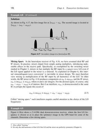
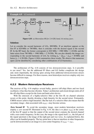
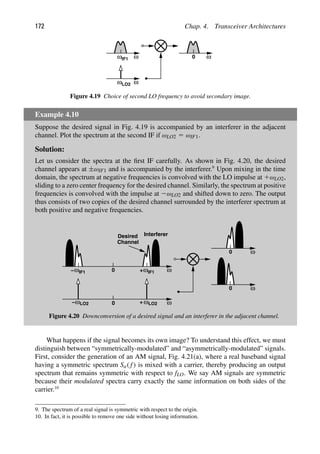
![Sec. 4.2. Receiver Architectures 173
ω
0 f
( (
S f
f LO f
( (
S f −f LO
f LO
VCO
f f
c
(a)
(b)
t
)
(t
xBB
Figure 4.21 (a) AM signal generation, (b) FM signal generation.
Now, consider an FM signal generated by a voltage-controlled oscillator [Fig. 4.21(b)]
(Chapter 8). We note that as the baseband voltage becomes more positive, the output fre-
quency, say, increases, and vice versa. That is, the information in the sideband below the
carrier is different from that in the sideband above the carrier. We say FM signals have an
asymmetric spectrum. Most of today’s modulation schemes, e.g., FSK, QPSK, GMSK, and
QAM, exhibit asymmetric spectra around their carrier frequencies. While the conceptual
diagram in Fig. 4.21(b) shows the asymmetry in the magnitude, some modulation schemes
may exhibit asymmetry in only their phase.
As exemplified by the spectra in Fig. 4.20, downconversion to a zero IF superimposes
two copies of the signal, thereby causing corruption if the signal spectrum is asymmetric.
Figure 4.22 depicts this effect more explicitly.
0 ω
ω
+ IF1
ωIF1
−
0 ω
Figure 4.22 Overlap of signal sidebands after second downconversion.
Example 4.11
Downconversion to what minimum intermediate frequency avoids self-corruption of asym-
metric signals?
Solution:
To avoid self-corruption, the downconverted spectra must not overlap each other. Thus, as
shown in Fig. 4.23, the signal can be downconverted to an IF equal to half of the signal
bandwidth. Of course, an interferer may now become the image.
(Continues)](https://image.slidesharecdn.com/rfmicroelectronicsrazavi-230814101614-71259b59/85/RF-MICROELECTRONICS_Razavi-pdf-198-320.jpg)
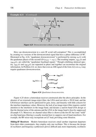
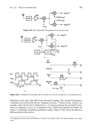
![176 Chap. 4. Transceiver Architectures
The receiver architecture of Fig. 4.26(a) has a number of interesting properties. To
translate an input frequency of fin to a second IF of zero, we must have
fLO1 1
1
2
fLO1 5 fin (4.8)
and hence
fLO1 5
2
3
fin. (4.9)
That is, for an input band spanning the range [ f1 f2], the LO must cover a range of [(2/3)f1
(2/3)f2] (Fig. 4.27). Moreover, the first IF in this architecture is not constant because
fIF1 5 fin 2 fLO (4.10)
5
1
3
fin. (4.11)
Thus, as fin varies from f1 to f2, fIF1 goes from f1/3 to f2/3 (Fig. 4.27). For this reason,
this topology is called the “sliding-IF architecture.” Unlike the conventional heterodyne
receiver of Fig. 4.16, where the first IF filter must exhibit a narrow bandwidth to per-
form some channel selection, this sliding IF topology requires a fractional (or normalized)
IF bandwidth12
equal to the RF input fractional bandwidth. This is because the former is
given by
BWIF,frac 5
1
3
f2 2
1
3
f1
1
3
f2 1
1
3
f1
/2
, (4.12)
and the latter,
BWRF,frac 5
f2 2 f1
( f2 1 f1)/2
. (4.13)
f
f 1 f
RF Range
f
LO Range
f1
2
3
2
3
f
2
2
f
f1
3 3
f2
First IF
Range
Figure 4.27 LO and IF ranges in the sliding-IF RX.
12. Fractional bandwidth is defined as the bandwidth of interest divided by the center frequency of the band.](https://image.slidesharecdn.com/rfmicroelectronicsrazavi-230814101614-71259b59/85/RF-MICROELECTRONICS_Razavi-pdf-201-320.jpg)
![Sec. 4.2. Receiver Architectures 177
Example 4.12
Suppose the input band is partitioned into N channels, each having a bandwidth of ( f2 2
f1)/N 5 f. How does the LO frequency vary as the receiver translates each channel to a
zero second IF?
Solution:
The first channel is located between f1 and f1 1 f. Thus the first LO frequency is chosen
equal to two-thirds of the center of the channel: fLO 5 (2/3)( f1 1 f/2). Similarly, for the
second channel, located between f1 1 f and f1 1 2 f, the LO frequency must be equal to
(2/3)( f1 1 3 f/2). In other words, the LO increments in steps of (2/3) f.
Example 4.13
With the aid of the frequency bands shown in Fig. 4.27, determine the image band for the
architecture of Fig. 4.26(a).
Solution:
For an LO frequency of (2/3)f1, the image lies at 2fLO 2 fin 5 f1/3. Similarly, if fLO1 5
(2/3)f2, then the image is located at f2/3. Thus, the image band spans the range [ f1/3 f2/3]
(Fig. 4.28). Interestingly, the image band is narrower than the input band.
f
f
f
1
Image Band
3
LO Band
RF Band
f 1 f 2
1 f
1
3 2
f
3 1 f
3 2
2 2
Figure 4.28 Image band in the sliding-IF RX.
Does this mean that the image for each channel is also narrower? No, recall from the
above example that the LO increments by (2/3) f as we go from one channel to the next.
Thus, consecutive image channels have an overlap of f/3.
The sliding-IF architecture may incorporate greater divide ratios in the generation of
the second LO from the first. For example, a ÷4 circuit produces quadrature outputs at
fLO1/4, leading to the following relationship
fLO1 1
1
4
fLO1 5 fin (4.14)](https://image.slidesharecdn.com/rfmicroelectronicsrazavi-230814101614-71259b59/85/RF-MICROELECTRONICS_Razavi-pdf-202-320.jpg)
![178 Chap. 4. Transceiver Architectures
and hence
fLO1 5
4
5
fin. (4.15)
The detailed spectra of such an architecture are studied in Problem 4.1. But we must
make two observations here. (1) With a ÷4 circuit, the second LO frequency is equal to
fin/5, slightly lower than that of the first sliding-IF architecture. This is desirable because
generation of LO quadrature phases at lower frequencies incurs smaller mismatches. (2)
Unfortunately, the use of a ÷4 circuit reduces the frequency difference between the image
and the signal, making it more difficult to reject the image and even the thermal noise of
the antenna and the LNA in the image band. In other words, the choice of the divide ratio
is governed by the trade-off between quadrature accuracy and image rejection.
Example 4.14
We wish to select a sliding-IF architecture for an 802.11g receiver. Determine the pros and
cons of a ÷2 or a ÷4 circuit in the LO path.
Solution:
With a ÷2 circuit, the 11g band (2.40–2.48 GHz) requires an LO range of 1.600–1.653 GHz
and hence an image range of 800–827 MHz [Fig. 4.29(a)]. Unfortunately, since the CDMA
transmit band begins at 824 MHz, such a sliding-IF receiver may experience a large image
in the range of 824–827 MHz.
f
Image Band
3
80
MHz
0.800 0.827 2.400 2.480
RF Band
80 MHz
f
Image Band
2.400 2.480
RF Band
80 MHz
20 MHz
1.440 1.488
(GHz) (GHz)
(a) (b)
Figure 4.29 Image band in an 11g RX with a (a) divide-by-2 circuit, (b) divide-by-4 circuit.
With a ÷4 circuit, the LO range is 1.920–1.984 GHz and the image range, 1.440–
1.488 GHz [Fig. 4.29(b)]. This image band is relatively quiet. (Only Japan has allocated a
band around 1.4 GHz to WCDMA.) Thus, the choice of the ÷4 ratio proves advantageous
here if the LNA selectivity can suppress the thermal noise in the image band. The first IF
is lower in the second case and may be beneficial in some implementations.
The baseband signals produced by the heterodyne architecture of Fig. 4.26(a) suffer
from a number of critical imperfections, we study these effects in the context of direct-
conversion architectures.](https://image.slidesharecdn.com/rfmicroelectronicsrazavi-230814101614-71259b59/85/RF-MICROELECTRONICS_Razavi-pdf-203-320.jpg)
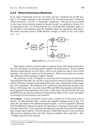
![180 Chap. 4. Transceiver Architectures
LNA
Pad
LO
Substrate
Figure 4.31 LO leakage.
Example 4.15
Determine the LO leakage from the output to the input of a cascode LNA.
Solution:
As depicted in Fig. 4.32(a), we apply a test voltage to the output and measure the voltage
delivered to the antenna, Rant. Considering only rO2 and CGD1 as the leakage path, we
M 1
R
(a)
M
r
Vb
C
R
Vant
VX
O2
D
VDD
GD1
2
g
g r
m2 2 O2
V
V2
Vant
Vant
m1
CGD1
R
Vant
VX
(b)
ant
ant
X
Figure 4.32 LO leakage in a cascode LNA.
construct the equivalent circuit shown in Fig. 4.32(b), note that the current flowing through
Rant and CGD1 is given by Vant/Rant, and write V2 5 2[Vant 1 Vant/(RantCGD1s)]. Thus, a
KCL at node X yields
Vant 1
Vant
RantCGD1s
gm2 1
Vant
Rant
1 gm1Vant 5
1
rO2
VX 2
Vant 1
Vant
RantCGD1s
. (4.16)
If gm2 1/rO2,
Vant
VX
≈
CGD1s
(gm1Rant 1 gm2Rant 1 1)CGD1s 1 gm2
·
Rant
rO2
. (4.17)](https://image.slidesharecdn.com/rfmicroelectronicsrazavi-230814101614-71259b59/85/RF-MICROELECTRONICS_Razavi-pdf-205-320.jpg)
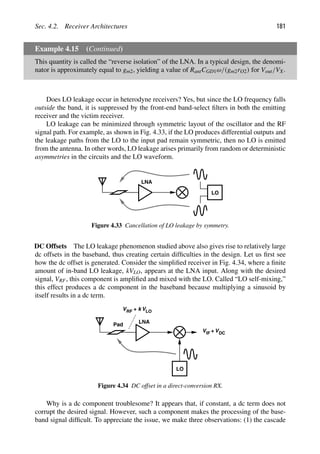
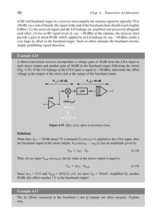
![Sec. 4.2. Receiver Architectures 183
Example 4.17 (Continued)
Solution:
Suppose, in the presence of the quadrature phases of the LO, the net LO leakage at the
input of the LNA is expressed as Vleak cos(ωLOt 1 φleak), where φleak arises from the phase
shift through the path(s) from each LO phase to the LNA input and also the summation of
the leakages VLO cos ωLOt and VLO sin ωLOt (Fig. 4.36). The LO leakage travels through
the LNA and each mixer, experiencing an additional phase shift, φckt, and is multiplied by
VLO cos ωLOt and VLO sin ωLOt. The dc components are therefore given by
Vdc,I 5 αVleakVLO cos(φleak 1 φckt) (4.20)
Vdc,Q 5 2αVleakVLO sin(φleak 1 φckt). (4.21)
Thus, the two dc offsets are generally unequal.
LNA
LO
Figure 4.36 Leakage of quadrature phases of LO.
Does the problem of dc offsets occur in heterodyne receivers having a zero second IF
[Fig. 4.26(a)]? Yes, the leakage of the second LO to the input of the IF mixers produces dc
offsets in the baseband. Since the second LO frequency is equal to fin/3 in Fig. 4.26(a), the
leakage is smaller than that in direct-conversion receivers,14
but the dc offset is still large
enough to saturate the baseband stages or at least create substantial nonlinearity.
The foregoing study implies that receivers having a final zero IF must incorporate some
means of offset cancellation in each of the baseband I and Q paths. A natural candidate is a
high-pass filter (ac coupling) as shown in Fig. 4.37(a), where C1 blocks the dc offset and R1
establishes proper bias, Vb, for the input of A1. However, as depicted in Fig. 4.37(b), such a
network also removes a fraction of the signal’s spectrum near zero frequency, thereby intro-
ducing intersymbol interference. As a rule of thumb, the corner frequency of the high-pass
filter, f1 5 (2πR1C1)21, must be less than one-thousandth of the symbol rate for negligi-
ble ISI. In practice, careful simulations are necessary to determine the maximum tolerable
value of f1 for a given modulation scheme.
The feasibility of on-chip ac coupling depends on both the symbol rate and the type
of modulation. For example, the bit rate of 271 kb/s in GSM necessitates a corner fre-
quency of roughly 20–30 Hz and hence extremely large capacitors and/or resistors. Note
14. Also because the LO in direct-conversion receivers employs inductors, which couple the LO waveform
into the substrate, whereas the second LO in heterodyne architectures is produced by an inductor-less divider.](https://image.slidesharecdn.com/rfmicroelectronicsrazavi-230814101614-71259b59/85/RF-MICROELECTRONICS_Razavi-pdf-208-320.jpg)
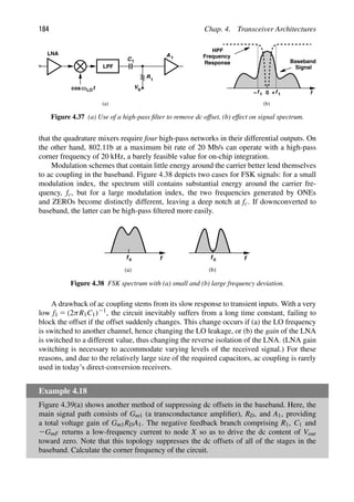
![Sec. 4.2. Receiver Architectures 185
Example 4.18 (Continued)
A 1
RD
R1
C1
VDD
in
V
X
GmF
Gm1
ω
out
V
in
V
R C
1
1 R C
1 1
1 + GmF
1
RD
A 1
G RD
A 1 m1
1 + GmF RD
A 1
G RD
A 1 m1
(a) (b)
Vout
−
Figure 4.39 (a) Offset cancellation by feedback, (b) resulting frequency response.
Solution:
Recognizing that the current returned by 2GmF to node X is equal to 2GmFVout/
(R1C1s 1 1) and the current produced by Gm1 is given by Gm1Vin, we sum the two at
node X, multiply the sum by RD and A1, and equate the result to Vout
2GmFVout
R1C1s 1 1
1 Gm1Vin
RDA1 5 Vout. (4.22)
It follows that
Vout
Vin
5
Gm1RDA1(R1C1s 1 1)
R1C1s 1 GmFRDA1 1 1
. (4.23)
The circuit thus exhibits a pole at 2(1 1 GmFRDA1)/(R1C1) and a zero at 21/(R1C1)
[Fig. 4.39(b)]. The input offset is amplified by a factor of Gm1RDA1/(1 1 GmFRDA1) ≈
Gm1/GmF if GmFRDA1 1. This gain must remain below unity, i.e., GmF is typically
chosen larger than Gm1. Unfortunately, the high-pass corner frequency is given by
f1 ≈
GmFRDA1
2π(R1C1)
, (4.24)
a factor of GmFRDA1 higher than that of the passive circuit in Fig. 4.37(a). This “active
feedback” circuit therefore requires greater values for R1 and C1 to provide a low f1.
The advantage is that C1 can be realized by a MOSFET [while that in Fig. 4.37(a)
cannot].
The most common approach to offset cancellation employs digital-to-analog converters
(DACs) to draw a corrective current in the same manner as the GmF stage in Fig. 4.39(a).
Let us first consider the cascade shown in Fig. 4.40(a), where I1 is drawn from node X](https://image.slidesharecdn.com/rfmicroelectronicsrazavi-230814101614-71259b59/85/RF-MICROELECTRONICS_Razavi-pdf-210-320.jpg)
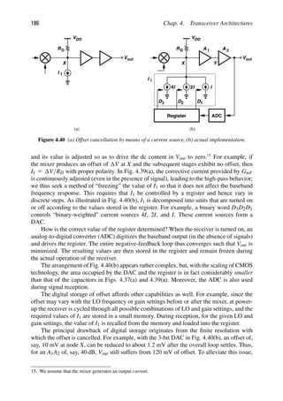
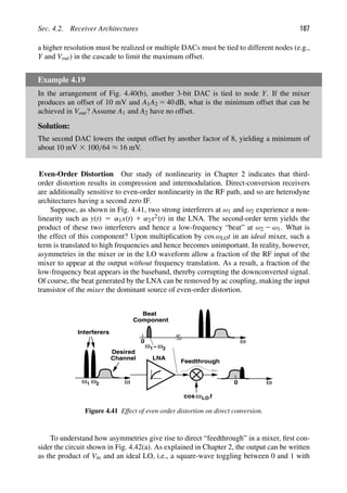
![188 Chap. 4. Transceiver Architectures
R
Vout1
LO
1
R
V
LO
1
out2
in
V
R
Vout1
LO
1
in
V
(a) (b)
Figure 4.42 (a) Simple mixer, (b) mixer with differential output.
50% duty cycle, S(t):
Vout(t) 5 Vin(t) · S(t) (4.25)
5 Vin(t) S(t) 2
1
2
1 Vin(t) ·
1
2
. (4.26)
We recognize that S(t) 2 1/2 represents a “dc-free” square wave consisting of only odd
harmonics. Thus, Vin(t) · [S(t) 2 1/2] contains the product of Vin and the odd harmonics of
the LO. The second term in (4.26), Vin(t) 3 1/2, denotes the RF feedthrough to the output
(with no frequency translation).
Next, consider the topology depicted in Fig. 4.42(b), where a second branch driven by
LO (the complement of LO) produces a second output. Expressing LO as 12S(t), we have
Vout1(t) 5 Vin(t)S(t) (4.27)
Vout2(t) 5 Vin(t)[1 2 S(t)]. (4.28)
As with Vout1(t), the second output Vout2(t) contains an RF feedthrough equal to Vin(t) 3
1/2 because 1 2 S(t) exhibits a dc content of 1/2. If the output is sensed differentially, the
RF feedthroughs in Vout1(t) and Vout2(t) are cancelled while the signal components add. It
is this cancellation that is sensitive to asymmetries; for example, if the switches exhibit a
mismatch between their on-resistances, then a net RF feedthrough arises in the differential
output.
The problem of even-order distortion is critical enough to merit a quantitative measure.
Called the “second intercept point” (IP2), such a measure is defined according to a two-tone
test similar to that for IP3 except that the output of interest is the beat component rather
than the intermodulation product. If Vin(t) 5 A cos ω1t 1A cos ω2t, then the LNA output is
given by
Vout(t) 5 α1Vin(t) 1 α2V2
in(t) (4.29)
5 α1A(cos ω1t 1 cos ω2t) 1 α2A2
cos(ω1 1 ω2)t
1 α2A2
cos(ω1 2 ω2)t 1 · · · , (4.30)](https://image.slidesharecdn.com/rfmicroelectronicsrazavi-230814101614-71259b59/85/RF-MICROELECTRONICS_Razavi-pdf-213-320.jpg)
![Sec. 4.2. Receiver Architectures 189
A
A
α1
A
α
A
A
in
(log scale)
IIP2
2
2
(log scale)
IIP2
Figure 4.43 Plot illustrating IP2.
Revealing that the beat amplitude grows with the square of the amplitude of the input
tones. Thus, as shown in Fig. 4.43, the beat amplitude rises with a slope of 2 on a log scale.
Since the net feedthrough of the beat depends on the mixer and LO asymmetries, the beat
amplitude measured in the baseband depends on the device dimensions and the layout and
is therefore difficult to formulate.
Example 4.20
Suppose the attenuation factor experienced by the beat as it travels through the mixer is
equal to k, whereas the gain seen by each tone as it is downconverted to the baseband is
equal to unity. Calculate the IP2.
Solution:
From Eq. (4.30), the value of A that makes the output beat amplitude, kα2A2, equal to the
main tone amplitude, α1A, is given by
kα2A2
IIP2 5 α1AIIP2 (4.31)
and hence
AIIP2 5
1
k
·
α1
α2
. (4.32)
Even-order distortion may manifest itself even in the absence of interferers. Suppose
in addition to frequency and phase modulation, the received signal also exhibits amplitude
modulation. For example, as explained in Chapter 3, QAM, OFDM, or simple QPSK with
baseband pulse shaping produce variable-envelope waveforms. We express the signal as
xin(t) 5 [A0 1 a(t)] cos[ωct 1 φ(t)], where a(t) denotes the envelope and typically varies
slowly, i.e., it is a low-pass signal. Upon experiencing second-order distortion, the signal
appears as
α2x2
in(t) 5 α2
A2
0 1 2A0a(t) 1 a2
(t)
1 1 cos[2ωct 1 2φ(t)]
2
. (4.33)](https://image.slidesharecdn.com/rfmicroelectronicsrazavi-230814101614-71259b59/85/RF-MICROELECTRONICS_Razavi-pdf-214-320.jpg)
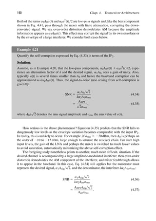
![Sec. 4.2. Receiver Architectures 191
Example 4.22
A desired signal at 2100 dBm is received along with an interferer [Aint 1 a(t)] cos[ωct 1
φ(t)], where Aint 5 5 mV and arms 5 1 mV. What IP2 is required to ensure SNR ≥ 20 dB?
Solution:
Since 2100 dBm is equivalent to a peak amplitude of Asig 5 3.16 μV, we have
AIIP2 5 SNR
Aintarms
Asig/
√
2
(4.38)
5 22.4 V (4.39)
5 137 dBm. (4.40)
Note that the interferer level (Aint 5 236 dBm) falls well below the compression point of
typical receivers, but it can still corrupt the signal if the IIP2 is not as high as 137 dBm.
This study reveals the relatively high IP2 values required in direct-conversion receivers.
We deal with methods of achieving a high IP2 in Chapter 6.
Flicker Noise Since linearity requirements typically limit the gain of the LNA/mixer
cascade to about 30 dB, the downconverted signal in a direct-conversion receiver is still
relatively small and hence susceptible to noise in the baseband circuits. Furthermore, since
the signal is centered around zero frequency, it can be substantially corrupted by flicker
noise. As explained in Chapter 6, the mixers themselves may also generate flicker noise at
their output.
In order to quantify the effect of flicker noise, let us assume the downconverted spec-
trum shown in Fig. 4.44, where fBW is half of the RF channel bandwidth. The flicker noise
is denoted by S1/f and the thermal noise at the end of the baseband by Sth. The frequency
at which the two profiles meet is called fc. We wish to determine the penalty due to flicker
f
fC
(log scale)
)
(
S f
1/f
Sth
fBW
fBW
1000
Figure 4.44 Spectrum for calculation of flicker noise.](https://image.slidesharecdn.com/rfmicroelectronicsrazavi-230814101614-71259b59/85/RF-MICROELECTRONICS_Razavi-pdf-216-320.jpg)
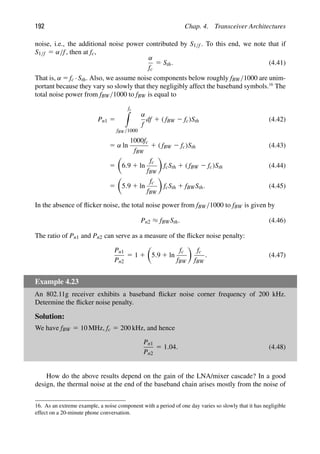
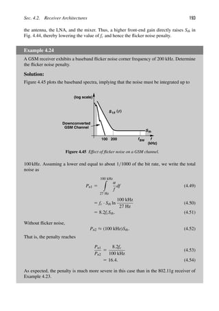
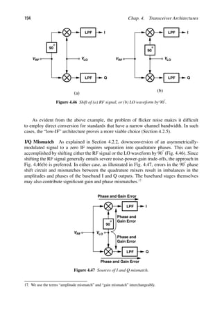
![Sec. 4.2. Receiver Architectures 195
Quadrature mismatches tend to be larger in direct-conversion receivers than in hetero-
dyne topologies. This occurs because (1) the propagation of a higher frequency (fin) through
quadrature mixers experiences greater mismatches; for example, a delay mismatch of 10 ps
between the two mixers translates to a phase mismatch of 188 at 5 GHz [Fig. 4.48(a)] and
3.68 at 1 GHz [Fig. 4.48(b)]; or (2) the quadrature phases of the LO itself suffer from greater
mismatches at higher frequencies; for example, since device dimensions are reduced to
achieve higher speeds, the mismatches between transistors increase.
LNA
t
cos
t
sinω
ω
ΔT = 10 ps
5 GHz
( (
t
xBB,I
( (
t
xBB,Q
LNA
LO1
5 GHz
4
4 GHz
1 GHz
ΔT = 10 ps
(a) (b)
LO
LO
Figure 4.48 Effect of a 10-ps propagation mismatch on a (a) direct-conversion and (b) heterodyne
receiver.
To gain insight into the effect of I/Q imbalance, consider a QPSK signal, xin(t) 5
a cos ωct 1 b sin ωct, where a and b are either 21 or 11. Now let us lump all of the gain
and phase mismatches shown in Fig. 4.47 in the LO path (Fig. 4.49)
xLO,I(t) 5 2
1 1
2
cos
ωct 1
θ
2
(4.55)
xLO,Q(t) 5 2
1 2
2
sin
ωct 2
θ
2
, (4.56)
2
ε
LPF
LPF
θ
2
+
1+
2
ε
θ
2
1−
90
−
( (
t
xBB,I
( (
t
xBB,Q
( (
t
xin
( (
t
xLO
Figure 4.49 Mismatches lumped in LO path.](https://image.slidesharecdn.com/rfmicroelectronicsrazavi-230814101614-71259b59/85/RF-MICROELECTRONICS_Razavi-pdf-220-320.jpg)
![196 Chap. 4. Transceiver Architectures
where the factor of 2 is included to simplify the results and and θ represent the amplitude
and phase mismatches, respectively. Multiplying xin(t) by the quadrature LO waveforms
and low-pass filtering the results, we obtain the following baseband signals:
xBB,I(t) 5 a
1 1
2
cos
θ
2
2 b
1 1
2
sin
θ
2
(4.57)
xBB,Q(t) 5 2a
1 2
2
sin
θ
2
1 b
1 2
2
cos
θ
2
. (4.58)
We now examine the results for two special cases: 5 0, θ 5 0 and 5 0, θ 5 0. In the
former case, xBB,I(t) 5 a(1 1 /2) and xBB,Q(t) 5 b(1 2 /2), implying that the quadrature
baseband symbols are scaled differently in amplitude [Fig. 4.50(a)]. More importantly, the
points in the constellation are displaced [Fig. 4.50(b)].
t
t
I
Q
Q
I
Ideal
(a) (b)
Figure 4.50 Effect of gain mismatch on (a) time-domain waveforms and (b) constellation of a QPSK
signal.
With 5 0 θ 5 0, we have xBB,I(t) 5 a cos(θ/2) 2 b sin(θ/2) and xBB,Q(t) 5
2a sin(θ/2) 1 b cos(θ/2). That is, each baseband output is corrupted by a fraction of the
data symbols in the other output [Fig. 4.51(a)]. Also, the constellation is compressed along
one diagonal and stretched along the other [Fig. 4.51(b)].
t
t
I
Q
Q
I
Ideal
(a) (b)
Figure 4.51 Effect of phase mismatch on (a) time-domain waveforms and (b) constellation of a
QPSK signal.](https://image.slidesharecdn.com/rfmicroelectronicsrazavi-230814101614-71259b59/85/RF-MICROELECTRONICS_Razavi-pdf-221-320.jpg)
![Sec. 4.2. Receiver Architectures 197
Example 4.25
An FSK signal is applied to a direct-conversion receiver. Plot the baseband waveforms and
determine the effect of I/Q mismatch.
Solution:
We express the FSK signal as xFSK(t) 5 A0 cos[(ωc 1 aω1)t], where a 5 ± 1 represents the
binary information; i.e., the frequency of the carrier swings by 1ω1 or 2ω1. Upon multi-
plication by the quadrature phases of the LO, the signal produces the following baseband
components:
xBB,I(t) 5 2A1 cos aω1t (4.59)
xBB,Q(t) 5 1A1 sin aω1t. (4.60)
Figure 4.52(a) illustrates the results: if the carrier frequency is equal to ωc 1 ω1 (i.e.,
a 5 11), then the rising edges of xBB,I(t) coincide with the positive peaks of xBB,Q(t).
t
)
(t
xFSK
)
(t
xBB,Q
)
(t
xBB,I
t
ωc+ ω1 ωc ω1
− ωc+ ω1 ωc ω1
−
LNA
LPF
LPF
t
cos
t
sinω
ω0
0
D
FF
)
(t
xBB,Q
)
(t
xBB,I
t
(c)
(a)
(b)
xBB,Q
xBB,I
Figure 4.52 (a) Baseband waveforms for an FSK signal, (b) FSK detection by a D flipflop,
(c) effect of phase and gain mismatches.
(Continues)](https://image.slidesharecdn.com/rfmicroelectronicsrazavi-230814101614-71259b59/85/RF-MICROELECTRONICS_Razavi-pdf-222-320.jpg)
![198 Chap. 4. Transceiver Architectures
Example 4.25 (Continued)
Conversely, if the carrier frequency is equal to ωc 2 ω1, then the rising edges of xBB,I(t)
coincide with the negative peaks of xBB,Q(t). Thus, the binary information is detected if
xBB,I(t) simply samples xBB,Q(t), e.g., by means of a D flipflop [Fig. 4.52(b)].
The waveforms of Fig. 4.52(a) and the detection method of Fig. 4.52(b) suggest that
FSK can tolerate large I/Q mismatches [Fig. 4.52(c)]: amplitude mismatch proves benign
so long as the smaller output does not suffer from degraded SNR, and phase mismatch is
tolerable so long as xBB,I(t) samples the correct polarity of xBB,Q(t). Of course, as the phase
mismatch approaches 908, the additive noise in the receive chain introduces errors.
In the design of an RF receiver, the maximum tolerable I/Q mismatch must be known
so that the architecture and the building blocks are chosen accordingly. For complex signal
waveforms such as OFDM with QAM, this maximum can be obtained by simulations: the
bit error rate is plotted for different combinations of gain and phase mismatches, providing
the maximum mismatch values that affect the performance negligibly. (The EVM can also
reflect the effect of these mismatches.) As an example, Fig. 4.53 plots the BER curves for a
system employing OFDM with 128 subchannels and QPSK modulation in each subchannel
[1]. We observe that gain/phase mismatches below 20.6 dB/68 have negligible effect.
In standards such as 802.11a/g, the required phase and gain mismatches are so small
that the “raw” matching of the devices and the layout may not suffice. Consequently, in
−2 0 4 6 8 10
10
0
10
−1
10
10
−2
−3
10
10
10
−4
−5
−6
BER
2
SNR (dB)
Figure 4.53 Effect of I/Q mismatch on an OFDM signal with QPSK modulation. (: no imbalance;
8: θ 5 68, 5 0.6 dB; : θ 5 108, 5 0.8 dB; : θ 5 168, 5 1.4 dB.)](https://image.slidesharecdn.com/rfmicroelectronicsrazavi-230814101614-71259b59/85/RF-MICROELECTRONICS_Razavi-pdf-223-320.jpg)
![Sec. 4.2. Receiver Architectures 199
LPF
LPF
I
Q
t
cos
t
sinω
ω
LNA
t
Amplitude
Mismatch
Mismatch
Phase
I
Q
LPF
LPF
t
cos
t
sinω
ω
LNA
ADC
ADC
Logic
(a)
(b)
LO
LO
LO
LO
φ
φ
Figure 4.54 (a) Computation and (b) correction of I/Q mismatch in a direct-conversion receiver.
many high-performance systems, the quadrature phase and gain must be calibrated—either
at power-up or continuously. As illustrated in Fig. 4.54(a), calibration at power-up can
be performed by applying an RF tone at the input of the quadrature mixers and observ-
ing the baseband sinusoids in the analog or digital domain [2]. Since these sinusoids can
be produced at arbitrarily low frequencies, their amplitude and phase mismatches can be
measured accurately. With the mismatches known, the received signal constellation is cor-
rected before detection. Alternatively, as depicted in Fig. 4.54(b), a variable-phase stage,
φ, and a variable-gain stage can be inserted in the LO and baseband paths, respectively,
and adjusted until the mismatches are sufficiently small. Note that the adjustment controls
must be stored digitally during the actual operation of the receiver.
Mixing Spurs Unlike heterodyne systems, direct-conversion receivers rarely encounter
corruption by mixing spurs. This is because, for an input frequency f1 to fall in the baseband
after experiencing mixing with nfLO, we must have f1 ≈ nfLO. Since fLO is equal to the
desired channel frequency, f1 lies far from the band of interest and is greatly suppressed by
the selectivity of the antenna, the band-select filter, and the LNA.
The issue of LO harmonics does manifest itself if the receiver is designed for a wide
frequency band (greater than two octaves). Examples include TV tuners, “software-defined
radios,” and “cognitive radios.”](https://image.slidesharecdn.com/rfmicroelectronicsrazavi-230814101614-71259b59/85/RF-MICROELECTRONICS_Razavi-pdf-224-320.jpg)
![200 Chap. 4. Transceiver Architectures
4.2.4 Image-Reject Receivers
Our study of heterodyne and direct-conversion receivers has revealed various pros and
cons. For example, heterodyning must deal with the image and mixing spurs and direct
conversion, with even-order distortion and flicker noise. “Image-reject” architectures are
another class of receivers that suppress the image without filtering, thereby avoiding the
trade-off between image rejection and channel selection.
908
Phase Shift Before studying these architectures, we must define a “shift-by-908”
operation. First, let us consider a tone, A cos ωct 5 (A/2)[exp(1jωct) 1 exp(2jωct)]. The
two exponentials respectively correspond to impulses at 1ωc and 2ωc in the frequency
domain. We now shift the waveform by 908:
A cos(ωct 2 908
) 5 A
e1j(ωct2908)
1 e2j(ωct2908)
2
(4.61)
5 2
A
2
je1jωct
1
A
2
je2jωct
(4.62)
5 A sin ωct. (4.63)
Equivalently, the impulse at 1ωc is multiplied by 2j and that at 2ωc, by 1j. We illustrate
this transformation in the three-dimensional diagram of Fig. 4.55(a), recognizing that the
impulse at 1ωc is rotated clockwise and that at 2ωc counterclockwise.
Similarly, for a narrowband modulated signal, x(t) 5 A(t) cos [ωct 1 φ(t)], we
perform a 908 phase shift as
A(t) cos[ωct 1 φ(t) 2 908
] 5 A(t)
e1j[ωct 1 φ(t)2908]
1 e2j[ωct 1 φ(t)2908]
2
(4.64)
5 A(t)
2je1j[ωct 1 φ(t)]
1 je2j[ωct 1 φ(t)]
2
(4.65)
5 A(t) sin[ωct 1 φ(t)]. (4.66)
ω
Re
Im
2
A
ωc
−
2
A
ωc
+
2
A
j
+
2
A
j
−
ω
Re
Im
ωc
−
ωc
+
( )
ω
X
( )
ω
X
j
( )
ω
X
( )
ω
X
j
−
(a) (b)
Figure 4.55 Illustration of 908 phase shift for (a) a cosine and (b) a modulated signal.](https://image.slidesharecdn.com/rfmicroelectronicsrazavi-230814101614-71259b59/85/RF-MICROELECTRONICS_Razavi-pdf-225-320.jpg)
![Sec. 4.2. Receiver Architectures 201
As depicted in Fig. 4.55(b), the positive-frequency contents are multiplied by 2j and
the negative-frequency contents by 1j (if ωc is positive). Alternatively, we write in the
frequency domain:
X908 (ω) 5 X(ω)[2jsgn(ω)], (4.67)
where sgn(ω) denotes the signum (sign) function. The shift-by-908 operation is also called
the “Hilbert transform.” The reader can prove that the Hilbert transform of the Hilbert
transform (i.e., the cascade of two 908 phase shifts) simply negates the original signal.
Example 4.26
In phasor diagrams, we simply multiply a phasor by 2j to rotate it by 908 clockwise. Is that
inconsistent with the Hilbert transform?
Solution:
No, it is not. A phasor is a representation of A exp( jωct), i.e., only the positive fre-
quency content. That is, we implicitly assume that if A exp( jωct) is multiplied by 2j, then
A exp(2jωct) is also multiplied by 1j.
The Hilbert transform, as expressed by Eq. (4.67), distinguishes between negative and
positive frequencies. This distinction is the key to image rejection.
Example 4.27
Plot the spectrum of A cos ωct 1 jA sin ωct.
Solution:
Multiplication of the spectrum of A sin ωct by j rotates both impulses by 908 coun-
terclockwise [Fig. 4.56(a)]. Upon adding this spectrum to that A cos ωct, we obtain the
ω
Re
Im
2
A ωc
−
2
A
ωc
+
2
A
j
+
2
A
j
−
(a)
(b)
−
+
ω
Re
Im
A
ωc
+
+
Figure 4.56 (a) A sine subjected to 908 phase shift, (b) spectrum of A cos ωct 1 j sin ωct.
(Continues)](https://image.slidesharecdn.com/rfmicroelectronicsrazavi-230814101614-71259b59/85/RF-MICROELECTRONICS_Razavi-pdf-226-320.jpg)
![202 Chap. 4. Transceiver Architectures
Example 4.27 (Continued)
one-sided spectrum shown in Fig. 4.56(b). This is, of course, to be expected because
A cos ωct1jA sin ωct 5 A exp(2jωct), whose Fourier transform is a single impulse located
at ω 5 1ωc.
Example 4.28
A narrowband signal I(t) with a real spectrum is shifted by 908 to produce Q(t). Plot the
spectrum of I(t) 1 jQ(t).18
Solution:
We first multiply I(ω) by 2jsgn(ω) [Fig. 4.57(a)] and then, in a manner similar to the pre-
vious example, multiply the result by j [Fig. 4.57(b)]. The spectrum of jQ(t) therefore
cancels that of I(t) at negative frequencies and enhances it at positive frequencies
[Fig. 4.57(c)]. The one-sided spectrum of I(t) 1 jQ(t) proves useful in the analysis of
transceivers.
ω
Re
Im
ωc
−
ωc
+
( )
ω
( )
ω
j
( )
ω
( )
ω
j
−
(a) (b)
I
I
I
I
ω
Re
Im
ωc
−
ωc
+
( )
ω
j
( )
ω
( )
ω
j
−
I
I
I
( )
ω
I
−
ω
Re
Im
ωc
+
( )
ω
I ( )
ω
j
+ Q
(c)
Figure 4.57 (a) 908 phase shift applied to I to produce Q, (b) multiplication of the result by j,
(c) analytic signal.
18. This sum is called the “analytic signal” of I(t).](https://image.slidesharecdn.com/rfmicroelectronicsrazavi-230814101614-71259b59/85/RF-MICROELECTRONICS_Razavi-pdf-227-320.jpg)
![Sec. 4.2. Receiver Architectures 203
V
V
out1
out2
Vin
C1
R1
R1
C1
ω
1
2
1
1
R1C1
HLPF
HHPF
ω
HHPF
2
π
+
2
π
−
HLPF
2
π
(a) (b)
0
Figure 4.58 (a) Use of an RC-CR network to perform a 908 phase shift, (b) frequency response of
the network.
How is the 908 phase shift implemented? Consider the RC-CR network shown in
Fig. 4.58(a), where the high-pass and low-pass transfer functions are respectively given
by
HHPF(s) 5
Vout1
Vin
5
R1C1s
R1C1s 1 1
(4.68)
HLPF(s) 5
Vout2
Vin
5
1
R1C1s 1 1
. (4.69)
The transfer functions exhibit a phase of ∠HHPF 5 π/2 2 tan21(R1C1ω) and ∠HLPF 5
2tan21(R1C1ω). Thus, ∠HHPF 2 ∠HLPF 5 π/2 at all frequencies and any choice of R1
and C1. Also, |Vout1/Vin| 5 |Vout2/Vin| 5 1/
√
2 at ω 5 (R1C1)21 [Fig. 4.58(b)]. We can
therefore consider Vout2 as the Hilbert transform of Vout1 at frequencies close to (R1C1)21.
Another approach to realizing the 908-phase-shift operation is illustrated in Fig. 4.59(a),
where the RF input is mixed with the quadrature phases of the LO so as to translate the
spectrum to a nonzero IF. As shown in Fig. 4.59(b), as a result of mixing with cos ωLOt,
the impulse at 2ωLO is convolved with the input spectrum around 1ωc, generating that at
2ωIF. Similarly, the impulse at 1ωLO produces the spectrum at 1ωIF from that at 2ωc.
Depicted in Fig. 4.59(c), mixing with sin ωLOt results in an IF spectrum at 2ωIF with a
coefficient 1j/2 and another at 1ωIF with a coefficient 2j/2. We observe that, indeed,
the IF spectrum emerging from the lower arm is the Hilbert transform of that from the
upper arm.](https://image.slidesharecdn.com/rfmicroelectronicsrazavi-230814101614-71259b59/85/RF-MICROELECTRONICS_Razavi-pdf-228-320.jpg)
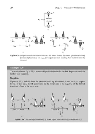
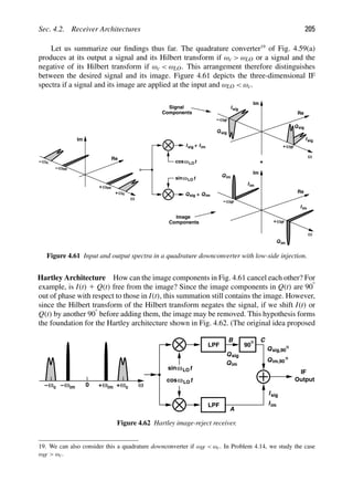
![206 Chap. 4. Transceiver Architectures
by Hartley relates to single-sideband transmitters [4].) The low-pass filters are inserted to
remove the unwanted high-frequency components generated by the mixers.
To understand the operation of Hartley’s architecture, we assume low-side injection
and apply a 908 phase shift to the Hilbert transforms of the signal and the image (the
Q arm) in Fig. 4.61, obtaining Qsig,908 and Qim,908 as shown in Fig. 4.63. Multiplication
of Qsig by 2jsgn(ω) rotates and superimposes the spectrum of Qsig on that of Isig (from
Fig. 4.61), doubling the signal amplitude. On the other hand, multiplication of Qim by
2jsgn(ω) creates the opposite of Iim, cancelling the image.
ω
Re
ω
+
ω
−
Im
IF
IF
sig
Q
Q
ω
Re
ω
+
ω
−
Im
IF
IF
Qim
sig,90
sig
Q
Qsig,90
Qim,90
Qim
Qim,90
(a) (b)
Figure 4.63 Spectra at points B and C in Hartley receiver.
In summary, the Hartley architecture first takes the negative Hilbert transform of the
signal and the Hilbert transform of the image (or vice versa) by means of quadrature mixing,
subsequently takes the Hilbert transform of one of the downconverted outputs, and sums the
results. That is, the signal spectrum is multiplied by [1jsgn(ω)][2jsgn(ω)] 5 11, whereas
the image spectrum is multiplied by [2jsgn(ω)][2jsgn(ω)] 5 21.
Example 4.30
An eager student constructs the Hartley architecture but with high-side injection. Explain
what happens.
Solution:
From Fig. 4.60, we note that the quadrature converter takes the Hilbert transform of the sig-
nal and the negative Hilbert transform of the image. Thus, with another 908 phase shift, the
outputs C and A in Fig. 4.62 contain the signal with opposite polarities and the image with
the same polarity. The circuit therefore operates as a “signal-reject” receiver! Of course,
the design is salvaged if the addition is replaced with subtraction.
The behavior of the Hartley architecture can also be expressed analytically. Let us rep-
resent the received signal and image as x(t) 5 Asig cos(ωct 1 φsig) 1 Aim cos(ωimt 1 φim),
where the amplitudes and phases are functions of time in the general case. Multiplying x(t)
by the LO phases and neglecting the high-frequency components, we obtain the signals at](https://image.slidesharecdn.com/rfmicroelectronicsrazavi-230814101614-71259b59/85/RF-MICROELECTRONICS_Razavi-pdf-231-320.jpg)
![Sec. 4.2. Receiver Architectures 207
points A and B in Fig. 4.62:
xA(t) 5
Asig
2
cos[(ωc 2 ωLO)t 1 φsig] 1
Aim
2
cos[(ωim 2 ωLO)t 1 φim] (4.70)
xB(t) 5 2
Asig
2
sin[(ωc 2 ωLO)t 1 φsig] 2
Aim
2
sin[(ωim 2 ωLO)t 1 φim], (4.71)
where a unity LO amplitude is assumed for simplicity. Now, xB(t) must be shifted by 908.
With low-side injection, the first sine has a positive frequency and becomes negative of
a cosine after the 908 shift (why?). The second sine, on the other hand, has a negative
frequency. We therefore write 2(Aim/2) sin[(ωim 2 ωLO)t 1 φim] 5 (Aim/2) sin[(ωLO 2
ωim)t 2 φim] so as to obtain a positive frequency and shift the result by 908, arriving at
2(Aim/2) cos[(ωLO 2 ωim)t 2 φim] 5 2(Aim/2) cos[(ωim 2 ωLO)t 1 φim]. It follows that
xC(t) 5
Asig
2
cos[(ωc 2 ωLO)t 1 φsig] 2
Aim
2
cos[(ωim 2 ωLO)t 1 φim]. (4.72)
Upon addition of xA(t) and xC(t), we retain the signal and reject the image.
The 908 phase shift depicted in Fig. 4.62 is typically realized as a 1458 shift in one path
and 2458 shift in the other (Fig. 4.64). This is because it is difficult to shift a single signal
by 908 while circuit components vary with process and temperature.
The principal drawback of the Hartley architecture stems from its sensitivity to mis-
matches: the perfect image cancellation described above occurs only if the amplitude and
phase of the negative of the image exactly match those of the image itself. If the LO
phases are not in exact quadrature or the gains and phase shifts of the upper and lower
arms in Fig. 4.64 are not identical, then a fraction of the image remains. To quantify
this effect, we lump the mismatches of the receiver as a single amplitude error, , and
phase error, θ, in the LO path, i.e., one LO waveform is expressed as sin ωLOt and
the other as (1 1 ) cos(ωLOt 1 θ). Expressing the received signal and image as x(t) 5
Asig cos(ωct 1 φsig) 1 Aim cos(ωimt 1 φim) and multiplying x(t) by the LO waveforms, we
write the downconverted signal at point A in Fig. 4.62 as
xA(t) 5
Asig
2
(1 1 ) cos[(ωc 2 ωLO)t 1 φsig 1 θ]
1
Aim
2
(1 1 ) cos[(ωim 2 ωLO)t 1 φim 1 θ]. (4.73)
RF
Input
IF
LPF
LPF
t
cosωLO
t
ωLO
sin
R1
R1
C1
C1
Output
Figure 4.64 Realization of 908 phase shift in Hartley receiver.](https://image.slidesharecdn.com/rfmicroelectronicsrazavi-230814101614-71259b59/85/RF-MICROELECTRONICS_Razavi-pdf-232-320.jpg)
![208 Chap. 4. Transceiver Architectures
The spectra at points B and C are still given by Eqs. (4.71) and (4.72), respectively. We
now add xA(t) and xC(t) and group the signal and image components at the output:
xsig(t) 5
Asig
2
(1 1 ) cos[(ωc 2 ωLO)t 1 φsig 1 θ]
1
Asig
2
cos[(ωc 2 ωLO)t 1 φsig] (4.74)
xim(t) 5
Aim
2
(1 1 ) cos[(ωim 2 ωLO)t 1 φim 1 θ]
2
Aim
2
cos[(ωim 2 ωLO)t 1 φim]. (4.75)
To arrive at a meaningful measure of the image rejection, we divide the image-to-signal
ratio at the input by the same ratio at the output.20
The result is called the “image rejection
ratio” (IRR). Noting that the average power of the vector sum a cos(ωt 1 α) 1 b cos ωt is
given by (a2 1 2ab cos α 1 b2)/2, we write the output image-to-signal ratio as
Pim
Psig
|out 5
A2
im
A2
sig
(1 1 )2 2 2(1 1 ) cos θ 1 1
(1 1 )2 1 2(1 1 ) cos θ 1 1
. (4.76)
Since the image-to-signal ratio at the input is given by A2
im/A2
sig, the IRR can be expressed
as
IRR 5
(1 1 )2 1 2(1 1 ) cos θ 1 1
(1 1 )2 2 2(1 1 ) cos θ 1 1
. (4.77)
Note that denotes the relative gain error and θ is in radians. Also, to express IRR in dB,
we must compute 10 log IRR (rather than 20 log IRR).
Example 4.31
If 1 rad, simplify the expression for IRR.
Solution:
Since cos θ ≈ 1 2 θ2/2 for θ 1 rad, we can reduce (4.77) to
IRR ≈
4 1 4 1 2 2 (1 1 ) θ2
2 1 (1 1 ) θ2
. (4.78)
In the numerator, the first term dominates and in the denominator 1, yielding
IRR ≈
4
2 1 θ2
. (4.79)
20. Note that the ratio of the output image power and the input image power is not meaningful because it
depends on the gain.](https://image.slidesharecdn.com/rfmicroelectronicsrazavi-230814101614-71259b59/85/RF-MICROELECTRONICS_Razavi-pdf-233-320.jpg)
![Sec. 4.2. Receiver Architectures 209
Example 4.31 (Continued)
For example, 5 10% (≈ 0.83 dB)21
limits the IRR to 26 dB. Similarly, θ 5 108 yields an
IRR of 21 dB. While such mismatch values may be tolerable in direct-conversion receivers,
they prove inadequate here.
With various mismatches arising in the LO and signal paths, the IRR typically falls
below roughly 35 dB. This issue and a number of other drawbacks limit the utility of the
Hartley architecture.
Another critical drawback, especially in CMOS technology, originates from the varia-
tion of the absolute values of R1 and C1 in Fig. 4.64. Recall from Fig. 4.58 that the phase
shift produced by the RC-CR network remains equal to 908 even with such variations, but
the output amplitudes are equal at only ω 5 (R1C1)21. Specifically, if R1 and C1 are nomi-
nally chosen for a certain IF, (R1C1)21 5 ωIF, but respectively experience a small change
of R and C with process or temperature, then the ratio of the output amplitudes of the
high-pass and low-pass sections is given by
HHPF
HLPF
5 (R1 1 R)(C1 1 C)ωIF (4.80)
≈ 1 1
R
R1
1
C
C1
. (4.81)
Thus, the gain mismatch is equal to
5
R
R1
1
C
C1
. (4.82)
For example, R/R1 5 20% limits the image rejection to only 20 dB. Note that these cal-
culations have assumed perfect matching between the high-pass and low-pass sections. If
the resistors or capacitors exhibit mismatches, the IRR degrades further.
Another drawback resulting from the RC-CR sections manifests itself if the signal
translated to the IF has a wide bandwidth. Since the gains of the high-pass and low-
pass sections depart from each other as the frequency departs from ωIF 5 (R1C1)21
[Fig. 4.58(b)], the image rejection may degrade substantially near the edges of the channel.
In Problem 4.17, the reader can prove that, at a frequency of ωIF 1 ω, the IRR is given by
IRR 5
ωIF
ω
2
. (4.83)
For example, a fractional bandwidth of 2 ω/ωIF 5 5% limits the IRR to 32 dB.
The limitation expressed by Eq. (4.83) implies that ωIF cannot be zero, dictating a het-
erodyne approach. Figure 4.65 shows an example where the first IF is followed by another
quadrature downconverter so as to produce the baseband signals. Unlike the sliding-IF
21. To calculate in dB, we write 20 log(1 1 10%) 5 0.83 dB.](https://image.slidesharecdn.com/rfmicroelectronicsrazavi-230814101614-71259b59/85/RF-MICROELECTRONICS_Razavi-pdf-234-320.jpg)
![210 Chap. 4. Transceiver Architectures
LPF
90
LPF
C
t
cosω
t
ω
sin
I
Q
t
cos
t
sinω
ω
RF
Input
LO2
LO2
LO1
LO1
Figure 4.65 Downconversion of Hartley receiver output to baseband.
architecture of Fig. 4.26(a), this topology also requires the quadrature phases of the first
LO, a critical disadvantage. The mixing spurs studied in Section 4.2.1 persist here as well.
The RC-CR sections used in Fig. 4.64 also introduce attenuation and noise. The 3-dB
loss resulting from |HHPF| 5 |HLPF| 5 1/
√
2 at ω 5 (R1C1)21 directly amplifies the noise
of the following adder. Moreover, the input impedance of each section, |R1 1 (C1s)21|,
reaches
√
2R1 at ω 5 (R1C1)21, imposing a trade-off between the loading seen by the
mixers and the thermal noise of the 908 shift circuit.
The voltage adder at the output of the Hartley architecture also poses difficulties as its
noise and nonlinearity appear in the signal path. Illustrated in Fig. 4.66, the summation is
typically realized by differential pairs, which convert the signal voltages to currents, sum
the currents, and convert the result to a voltage.
M M
1 2
Vout
Vin1
M M
Vin2
3 4
RD
VDD
RD
Figure 4.66 Summation of two voltages.
Weaver Architecture Our analysis of the Hartley architecture has revealed several issues
that arise from the use of the RC-CR phase shift network. The Weaver receiver, derived
from its transmitter counterpart [5], avoids these issues.
As recognized in Fig. 4.59, mixing a signal with quadrature phases of an LO takes the
Hilbert transform. Depicted in Fig. 4.67, the Weaver architecture replaces the 908 phase
shift network with quadrature mixing. To formulate the circuit’s behavior, we begin with
xA(t) and xB(t) as given by Eqs. (4.70) and (4.71), respectively, and perform the second](https://image.slidesharecdn.com/rfmicroelectronicsrazavi-230814101614-71259b59/85/RF-MICROELECTRONICS_Razavi-pdf-235-320.jpg)
![Sec. 4.2. Receiver Architectures 211
LPF
LPF
A
B
RF
Input
IF
Output
C
D
t
cosω
t
ω
sin 1
1 t
cosω
t
ω
sin 2
2
LPF
LPF
E
F
Figure 4.67 Weaver architecture.
quadrature mixing operation, arriving at
xC(t) 5
Asig
4
cos[(ωc 2 ω1 2 ω2)t 1 φsig] 1
Aim
4
cos[(ωim 2 ω1 2 ω2)t 1 φim]
1
Asig
4
cos[(ωc 2 ω1 1 ω2)t 1 φsig] 1
Aim
4
cos[(ωim 2 ω1 1 ω2)t 1 φim]
(4.84)
xD(t) 5 2
Asig
4
cos[(ωc 2 ω1 2 ω2)t 1 φsig] 2
Aim
4
cos[(ωim 2 ω1 2 ω2)t 1 φim]
1
Asig
4
cos[(ωc 2 ω1 1 ω2)t 1 φsig] 1
Aim
4
cos[(ωim 2 ω1 1 ω2)t 1 φim].
(4.85)
Should these results be added or subtracted? Let us assume low-side injection for both
mixing stages. Thus, ωim ω1 and ω1 2ωim ω2 (Fig. 4.68). Also, ω1 2ωim 1ω2 ω1 2
ωim 2ω2. The low-pass filters following points C and D in Fig. 4.67 must therefore remove
the components at ω1 2 ωim 1 ω2 (5 ωc 2 ω1 1 ω2), leaving only those at ω1 2 ωim 2 ω2
(5 ωc 2 ω1 2 ω2). That is, the second and third terms in Eqs. (4.84) and (4.85) are filtered.
Upon subtracting xF(t) from xE(t), we obtain
xE(t) 2 xF(t) 5
Asig
2
cos[(ωc 2 ω1 2 ω2)t 1 φsig]. (4.86)
The image is therefore removed. In Problem 4.19, we consider the other three combinations
of low-side and high-side injection so as to determine whether the outputs must be added
or subtracted.
ω
ωc
ωim ω1 ω
ω
ω
0 2 ω
−
1 im
Figure 4.68 RF and IF spectra in Weaver architecture.](https://image.slidesharecdn.com/rfmicroelectronicsrazavi-230814101614-71259b59/85/RF-MICROELECTRONICS_Razavi-pdf-236-320.jpg)
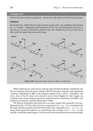
![Sec. 4.2. Receiver Architectures 213
ω
0
ω
0
ω
0
RF
Input
First
IF
IF
Second
Image
Desired
Channel
Secondary
1
ω
ω
2ω2 1
ωin
ωin
ω2
ω1
ωin
ω1
ωin ω2
ω
2ω2 1
ωin
2
Figure 4.70 Secondary image in Weaver architecture.
LPF
LPF
RF
Input t
cosω
t
ω
sin 1
1
2
)
(t
xBB,I
)
(t
xBB,Q
Figure 4.71 Double quadrature downconversion Weaver architecture to produce baseband outputs.
produces a zero IF, in which case it must perform quadrature separation as well. Figure 4.71
shows an example [6], where the second LO is derived from the first by frequency division.
The Weaver topology also suffers from mixing spurs in both downconversion steps. In
particular, the harmonics of the second LO frequency may downconvert interferers from
the first IF to baseband.
Calibration For image-rejection ratios well above 40 dB, the Hartley or Weaver archi-
tectures must incorporate calibration, i.e., a method of cancelling the gain and phase
mismatches. A number of calibration techniques have been reported [7, 9].](https://image.slidesharecdn.com/rfmicroelectronicsrazavi-230814101614-71259b59/85/RF-MICROELECTRONICS_Razavi-pdf-238-320.jpg)
![214 Chap. 4. Transceiver Architectures
4.2.5 Low-IF Receivers
In our study of heterodyne receivers, we noted that it is undesirable to place the image
within the signal band because the image thermal noise of the antenna, the LNA, and the
input stage of the RF mixer would raise the overall noise figure by approximately 3 dB.22
In
“low-IF receivers,” the image indeed falls in the band but is suppressed by image rejection
operations similar to those described in Section 4.2.4. To understand the motivation for the
use of low-IF architectures, let us consider a GSM receiver as an example. As explained in
Section 4.2.3, direct conversion of the 200-kHz desired channel to a zero IF may signifi-
cantly corrupt the signal by 1/f noise. Furthermore, the removal of the dc offset by means
of a high-pass filter proves difficult. Now suppose the LO frequency is placed at the edge
of the desired (200-kHz) channel [Fig. 4.72(a)], thereby translating the RF signal to an
IF of 100 kHz. With such an IF, and because the signal carries little information near the
edge, the 1/f noise penalty is much less severe. Also, on-chip high-pass filtering of the
signal becomes feasible. Called a “low-IF receiver,” this type of system is particularly
attractive for narrow-channel standards.
f
fc
f
fLO
f
0 100 kHz
200 kHz
f
fc
9 dB
Adjacent
Channel
(a (
) b)
Figure 4.72 (a) Spectra in a low-IF receiver, (b) adjacent-channel specification in GSM.
The heterodyne downconversion nonetheless raises the issue of the image, which in
this case falls in the adjacent channel. Fortunately, the GSM standard requires that receivers
tolerate an adjacent channel only 9 dB above the desired channel (Chapter 3) [Fig. 4.72(b)].
Thus, an image-reject receiver with a moderate IRR can lower the image to well below the
signal level. For example, if IRR 5 30 dB, the image remains 21 dB below the signal.
Example 4.33
Repeat Example 4.24 for a low-IF receiver.
Solution:
Assuming that high-pass filtering of dc offsets also removes the flicker noise up to roughly
20 kHz, we integrate the noise from 20 kHz to 200 kHz (Fig. 4.73):
22. This occurs because the entire signal band must see a flat frequency response in the antenna/LNA/mixer
chain.](https://image.slidesharecdn.com/rfmicroelectronicsrazavi-230814101614-71259b59/85/RF-MICROELECTRONICS_Razavi-pdf-239-320.jpg)
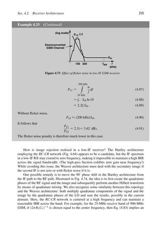
![216 Chap. 4. Transceiver Architectures
IF
Output
t
cosω
t
ω
sin 2
2
LPF
LPF
RF
Input
R1
R1
C1
C1
Quadrature Phases of
Image and Signal
Figure 4.74 Quadrature phase separation in RF path of a Hartley receiver.
IRR of 20 log(900 MHz/12.5 MHz) 5 37 dB. However, the variation of R1 and C1 still
limits the IRR to about 20 dB [Eq. (4.82)].
Another variant of the low-IF architecture is shown in Fig. 4.75. Here, the downcon-
verted signals are applied to channel-select filters and amplifiers as in a direct-conversion
receiver.23
The results are then digitized and subjected to a Hilbert transform in the digital
domain before summation. Avoiding the issues related to the analog 908 phase shift opera-
tion, this approach proves a viable choice. Note that the ADCs must accommodate a signal
bandwidth twice that in a direct-conversion receiver, thus consuming higher power. This
issue is unimportant in narrow-channel standards such as GSM because the ADC power
dissipation is but a small fraction of that of the overall system.
LPF
90
LPF
t
cosωLO
t
ωLO
sin
ADC
ADC
)
(t
xRF
Figure 4.75 Low-IF receiver with 908 phase shift in digital domain.
Let us summarize our thoughts thus far. If a low-IF receiver places the image in the
adjacent channel, then it cannot employ an RC-CR 908 phase shift after downconversion.
Also, a 908 circuit in the RF path still suffers from RC variation. For these reasons, the
concept of “low IF” can be extended to any downconversion that places the image within
23. The channel-select filters must, however, provide a bandwidth equal to the RF signal bandwidth rather than
half of it [Fig. 4.72(a)].](https://image.slidesharecdn.com/rfmicroelectronicsrazavi-230814101614-71259b59/85/RF-MICROELECTRONICS_Razavi-pdf-241-320.jpg)
![Sec. 4.2. Receiver Architectures 217
the band so that the IF is significantly higher than the signal bandwidth, possibly allowing
the use of an RC-CR network—but not so high as to unduly burden the ADC. Of course,
since the image no longer lies in the adjacent channel, a substantially higher IRR may be
required. Some research has therefore been expended on low-IF receivers with high image
rejection. Such receivers often employ “polyphase filters” (PPFs) [10, 11].
Polyphase Filters Recall from Section 4.2.4 that heterodyne quadrature downconver-
sion subjects the signal to low-side injection and the image to high-side injection, or vice
versa, thus creating the Hilbert transform of one and the negative Hilbert transform of the
other. Now let us consider the circuit shown in Fig. 4.76(a), where Vout can be viewed as a
weighted sum of V1 and V2:
Vout 5
V1 1 R1C1sV2
R1C1s 1 1
. (4.92)
R1 C1
V V
out
V
R1 C1
out
V
V1 1
jV
V2 = −
V1
1
jV
V2 = −
out
V
R1 C1
out
V
V1 1
jV
V2
V1
1
jV
V2
out
V
= +
(c)
(a)
(b)
1 2
= +
= 0
Figure 4.76 (a) Simple RC circuit, (b) output in response to V1 and 2jV1, (c) output in response to
V1 and 1jV1.
We consider two special cases.
1. The voltage V2 is the Hilbert transform of V1; in phasor form, V2 5 2jV1 (Example
4.26). Consequently, for s 5 jω,
Vout 5 V1
R1C1ω 1 1
jR1C1ω 1 1
. (4.93)
If ω 5 (R1C1)21, then Vout 5 2V1/(1 1 j) 5 V1(1 2 j). That is, |Vout| 5
√
2V1
and ∠Vout 5 ∠Vin 2 458 [Fig. 4.76(b)]. In this case, the circuit simply computes
the vector summation of V1 and V2 5 2jV1. We say the circuit rotates by 2458 the
voltage sensed by the resistor.
2. The voltage V2 is the negative Hilbert transform of V1, i.e., V2 5 1jV1. For s 5 jω,
Vout 5 V1
2R1C1ω 1 1
jR1C1ω 1 1
. (4.94)](https://image.slidesharecdn.com/rfmicroelectronicsrazavi-230814101614-71259b59/85/RF-MICROELECTRONICS_Razavi-pdf-242-320.jpg)
![218 Chap. 4. Transceiver Architectures
Interestingly, if ω 5 (R1C1)21, then Vout 5 0 [Fig. 4.76(c)]. Intuitively, we can
say that C1 rotates V2 by another 908 so that the result cancels the effect of V1
at the output node. The reader is encouraged to arrive at these conclusions using
superposition.
In summary, the series branch of Fig. 4.76(a) rotates V1 by 2458 (to produce Vout) if
V2 5 2jV1 and rejects V1 if V2 5 1jV1. The circuit can therefore distinguish between the
signal and the image if it follows a quadrature downconverter.
Example 4.34
Extend the topology of Fig. 4.76(a) if V1 and 2jV1 are available in differential form and
construct an image-reject receiver.
Solution:
Figure 4.77(a) shows the arrangement and the resulting phasors if R1 5 R2 5 R and
C1 5 C2 5 C. The connections to quadrature downconversion mixers are depicted in
Fig. 4.77(b).
R1 C1
V
V1 1
jV
V2 = −
V1
1
jV
V
1
jV
V2
1
jV
(a)
+
out1
Vout2
R C
V1
− = +
+
out1
Vout2
−
t
cos
t
sinω
ωLO
LO
VRF
R1
C1
out
V
R
C2
2
Vsig
+ Vim
Vsig V
− im
−
+
sig
+ im
jV −jV
sig im
jV jV
− +
(b)
+
V1
−
2 2
Figure 4.77 (a) RC circuit sensing differential inputs, (b) quadrature downconverter driving
RC network of part (a).](https://image.slidesharecdn.com/rfmicroelectronicsrazavi-230814101614-71259b59/85/RF-MICROELECTRONICS_Razavi-pdf-243-320.jpg)
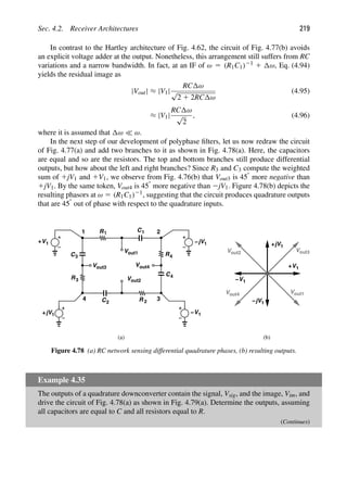
![220 Chap. 4. Transceiver Architectures
Example 4.35 (Continued)
1
jV
V
+
out1
Vout2
−
V
−
Vout3
Vout4
t
cos
t
sinω
ωLO
LO
VRF
R1
C1
V
R
C2
2
Vsig
+ Vim
Vsig V
− im
−
+
sig
+ im
jV −jV
sig im
jV jV
− +
3
4
2
out1 Vout2
R
C
Vout3
3
3
R
C
V
4
4
out4
sig
jVsig
sig
1
3
4
2
Vsig
+
jV
+
−
V
−
jV
1
3
V
+
2
4
Vout1 V
= = = 0
(c)
(a)
(b)
im
im
im
im
out4
Figure 4.79 (a) Quadrature downconverter driving RC sections, (b) resulting signal output, (c)
resulting image output.
Solution:
The quadrature downconverter produces 1Vsig 1 Vim, 2Vsig 2 Vim, 1jVsig 2 jVim, and
2jVsig 1 jVim. At ω 5 (RC)21, the branch R1C1 rotates 1Vsig by 2458 to generate Vout1.
Similarly, R2C2 rotates 2Vsig by 458 to generate Vout2, etc. [Fig. 4.79(b)]. The image
components, on the other hand, yield a zero output [Fig. 4.79(c)]. The key point here is that,
if we consider the sequence of nodes 1, 2, 3, and 4, we observe that Vsig rotates clockwise by](https://image.slidesharecdn.com/rfmicroelectronicsrazavi-230814101614-71259b59/85/RF-MICROELECTRONICS_Razavi-pdf-245-320.jpg)
![Sec. 4.2. Receiver Architectures 221
Example 4.35 (Continued)
908 from one node to the next, whereas Vim rotates counterclockwise by 908 from one node
to the next. The circuit therefore exhibits an asymmetry in its response to the “sequence”
of the four inputs.
The multiphase circuit of Fig. 4.78(a) is called a “sequence-asymmetric polyphase
filter” [8]. Since the signal and the image arrive at the inputs with different sequences, one
is passed to the outputs while the other is suppressed. But what happens if ω 5 (RC)21?
Substituting ω 5 (R1C1)21 1 ω in Eq. (4.93), we have
Vout1 5 Vsig
2 1 RC ω
1 1 j(1 1 RC ω)
, (4.97)
and hence,
|Vout1|2
5 |Vsig|2 4 1 4RC ω 1 R2C2 ω2
2 1 2RC ω 1 R2C2 ω2
(4.98)
≈ 2|Vsig|2
1 1 RC ω 1
R2C2 ω2
4
1 2 RC ω 2
R2C2 ω2
2
(4.99)
≈ 2|Vsig|2
1 2
5
4
R2
C2
ω2
. (4.100)
That is,
|Vout1| ≈
√
2|Vsig|
1 2
5
8
R2
C2
ω2
. (4.101)
The phase of Vout1 is obtained from (4.97) as
∠Vout1 5 ∠Vsig 2 tan21
(1 1 RC ω). (4.102)
Since tan21(1 1 RC ω) ≈ π/4 1 RC ω/2 for RC ω 1 rad,
∠Vout1 5 ∠Vsig 2
π
4
1
RC ω
2
. (4.103)
Figure 4.80(a) illustrates the effect on all four phases of the signal, implying that the outputs
retain their differential and quadrature relationship.
For the image, we return to Eq. (4.96) and note that the four outputs have a magnitude
equal to VimRC ω/
√
2 and phases similar to those of the signal components in Fig. 4.80(a).
The output image phasors thus appear as shown in Fig. 4.80(b). The reader is encouraged
to prove that Vout1 is at 2458 2 RC ω/2 and Vout3 at 21358 2 RC ω/2.
An interesting observation in Fig. 4.80 is that the output signal and image components
exhibit opposite sequences [10, 11]. We therefore expect that if this polyphase filter is](https://image.slidesharecdn.com/rfmicroelectronicsrazavi-230814101614-71259b59/85/RF-MICROELECTRONICS_Razavi-pdf-246-320.jpg)
![222 Chap. 4. Transceiver Architectures
Vout1
Vout2
Vout3
Vout4
RC Δω
2
Vout1
Vout2
V
V
(a) (b)
out4
out3
Figure 4.80 Effect of polyphase filter at a frequency offset of ω for (a) signal, and (b) image.
V
V 1
jV
+
out1
Vout2
C
Vout4
Vout3
2
1 −
1
jV
+ V1
−
1 2
3
4
(a)
VA
VB
(b)
VC
VD
Figure 4.81 (a) Cascaded polyphase sections, (b) alternative drawing.
followed by another, then the image can be further suppressed. Figure 4.81(a) depicts such
a cascade and Fig. 4.81(b) shows an alternative drawing that more easily lends itself to
cascading.
We must now answer two questions: (1) how should we account for the loading of the
second stage on the first? (2) how are the RC values chosen in the two stages? To answer
the first question, consider the equivalent circuit shown in Fig. 4.82, where Z1-Z4 represent
the RC branches in the second stage. Intuitively, we note that Z1 attempts to “pull” the
phasors Vout1 and Vout3 toward each other, Z2 attempts to pull Vout1 and Vout4 toward each
other, etc. Thus, if Z1 5 · · · 5 Z4 5 Z, then, Vout1–Vout4 experience no rotation, but the
loading may reduce their magnitudes. Since the angles of Vout1–Vout4 remain unchanged,
we can express them as ±α(1 ± j)V1, where α denotes the attenuation due to the loading
of the second stage. The currents drawn from node X by Z1 and Z2 are therefore equal to
[α(1 2 j)V1 2 α(1 1 j)V1]/Z1 and [α(1 2 j)V1 1 α(1 1 j)V1]/Z2, respectively. Summing](https://image.slidesharecdn.com/rfmicroelectronicsrazavi-230814101614-71259b59/85/RF-MICROELECTRONICS_Razavi-pdf-247-320.jpg)
![Sec. 4.2. Receiver Architectures 223
V
V 1
jV
+
out1
Vout2
Vout4
Vout3
1 −
1
jV
+ V1
−
Z1 Z2
Z Z
4 3
X
Figure 4.82 Effect of loading of second polyphase section.
all of the currents flowing out of node X and equating the result to zero, we have
α(1 2 j)V1 2 V1
R
1 [α(1 2 j)V1 1 jV1]Cjω 1
α(1 2 j)V1 2 α(1 1 j)V1
Z
1
α(1 2 j)V1 1 α(1 1 j)V1
Z
5 0. (4.104)
This equality must hold for any nonzero value of V1. If RCω 5 1, the expression reduces to
2α 2 2 1
2α(1 2 j)R
Z
5 0. (4.105)
That is,
α 5
Z
Z 1 (1 2 j)R
. (4.106)
For example, if Z 5 R 1 ( jCω)21, then α 5 1/2, revealing that loading by an identical
stage attenuates the outputs of the first stage by a factor of 2.
Example 4.36
If Z 5 R 1 ( jCω)21 and RCω 5 1, determine VA in Fig. 4.81(a).
Solution:
We have Vout1 5 (1/2)(1 2 jV1) and Vout4 5 (1/2)(21 2 j)V1, observing that Vout1 and
Vout2 have the same phase relationship as V1 and V2 in Fig. 4.76(b). Thus, VA is simply the
vector sum of Vout1 and Vout4:
VA 5 2jV1. (4.107)
In comparison with Fig. 4.76(b), we note that a two-section polyphase filter produces an
output whose magnitude is
√
2 times smaller than that of a single-section counterpart. We
say each section attenuates the signal by a factor of
√
2.](https://image.slidesharecdn.com/rfmicroelectronicsrazavi-230814101614-71259b59/85/RF-MICROELECTRONICS_Razavi-pdf-248-320.jpg)
![224 Chap. 4. Transceiver Architectures
The second question relates to the choice of RC values. Suppose both stages employ
RC 5 R0C0. Then, the cascade of two stages yields an image attenuation equal to the square
of Eq. (4.95) at a frequency of (R0C0)21 1 ω:
|
Vim,out
Vim,in
| ≈
(R0C0 ω)2
2 1 2R0C0 ω
, (4.108)
which reduces to (R0C0 ω)2/2 for ω (R0C0)21. Figure 4.83 plots this behavior,
comparing it with that of a single section.
Δω
R0 C0
2
Vim,out
Vim,in Two−Stage
PPF
PPF
Single−Stage
Figure 4.83 Image rejection for single-stage and two-stage polyphase filters.
What happens if the two stages use different time constants? In particular, for a given
IF of ω0, let us assume that the time constants in the first and second stages are respectively
equal to R1C1 and R2C2 such that ω0 2 (R1C1)21 5 (R2C2)21 2 ω0, i.e., the center fre-
quencies are shifted up and down. From Eq. (4.96), we plot the image rejections of the two
stages as shown in Fig. 4.84(a).24
The product of these two functions is a parabola cross-
ing zero at ω1 5 (R1C1)21 and ω2 5 (R2C2)21 [Fig. 4.84(b)]. The reader can prove that
the attenuation at ω0 is equal to (ω1 2 ω2)2/(8ω1ω2), which must be chosen sufficiently
small. The reader can also show that for an attenuation of 60 dB, ω1 2 ω2 cannot exceed
approximately 18% of ω0.
The advantage of splitting the cut-off frequencies of the two stages is the wider
achievable bandwidth. Figure 4.85 plots the image rejection for ω1 5 ω2 5 ω0 and ω1 5 ω2.
The cascading of polyphase filter sections entails both attenuation and additional ther-
mal noise. To alleviate the former, the resistors in the latter stages can be chosen larger than
those in the former, but at the cost of higher noise. For this reason, polyphase filters are
only occasionally used in RF receivers. In low-IF architectures, the polyphase filters can
be realized as “complex filters” so as to perform channel-selection filtering [12].
Double-Quadrature Downconversion In our study of the Hartley architecture, we noted
that mismatches arise in both the RF signal path and the LO path. A method of reducing the
effect of mismatches incorporates “double-quadrature” downconversion [10]. Illustrated
in Fig. 4.86, the circuit decomposes the RF signal into quadrature components, performs
24. For clarity, the plots are allowed to be negative even though Eq. (4.96) contains absolute values.](https://image.slidesharecdn.com/rfmicroelectronicsrazavi-230814101614-71259b59/85/RF-MICROELECTRONICS_Razavi-pdf-249-320.jpg)
![Sec. 4.2. Receiver Architectures 225
ω
R C
1
2 2
Image Rejection
of Second Stage
R C
1
Image Rejection
of First Stage
1 1
ω
R C
1
2 2
R C
1
1 1
ω0
Casade
Image Rejection
ω
R C
1
2 2
R C
1
1 1
ω0
Image Rejection
Magnitude of Casade
(c)
(a)
(b)
Figure 4.84 (a) Image rejections of two unidentical polyphase stages, (b) cascade image rejection,
(c) magnitude of cascade image rejection.
ω
R C
1
2 2
R C
1
1 1
ω0
Image Rejection
ω =
1 ω =
2 ω0
ω =
1 ω2
BW1
BW2
Figure 4.85 Comparison of image rejections of two identical and unidentical polyphase stages.
quadrature downconversion on each of the RF components, and subtracts and adds the
results to produce net quadrature IF outputs. It can be shown [10] that the overall gain and
phase mismatches of this topology are given by
A
A
5
ARF
ARF
·
ALO
ALO
1
Gmix
Gmix
(4.109)
tan( φ) 5 tan( φRF) · tan( φLO) 1
tan( φmix)
2
, (4.110)](https://image.slidesharecdn.com/rfmicroelectronicsrazavi-230814101614-71259b59/85/RF-MICROELECTRONICS_Razavi-pdf-250-320.jpg)
![226 Chap. 4. Transceiver Architectures
t
ω
t
c
c
t
cosω
t
sin c
c
ω
90
RF
Input
I
Q
cos
sin
ω
Figure 4.86 Low-IF receiver with double quadrature downconverter.
where ARF/ARF and ALO/ALO denote amplitude mismatches in the RF and LO paths,
respectively, and φRF and φLO are the corresponding phase mismatches. The quantities
Gmix/Gmix and φmix denote the conversion gain mismatch and phase mismatch of the
mixers, respectively. Thus, the IRR is only limited by mixer mismatches because the first
terms on the right-hand sides of (4.109) and (4.110) are very small.
Equations (4.109) and (4.110) reveal that the IRR of the double-quadrature architec-
ture is likely to fall well below 60 dB. This is because, even with no phase mismatch,
Gmix/Gmix must remain less than 0.1% for IRR 5 60 dB, a very stringent requirement
even for matching of simple resistors. Calibration of the mismatches can therefore raise the
IRR more robustly [7, 9].
4.3 TRANSMITTER ARCHITECTURES
4.3.1 General Considerations
An RF transmitter performs modulation, upconversion, and power amplification. In most of
today’s systems, the data to be transmitted is provided in the form of quadrature baseband
signals. For example, from Chapter 3 the GMSK waveform in GSM can be expanded as
xGMSK(t) 5 A cos[ωct 1 m
xBB(t) ∗ h(t)dt] (4.111)
5 A cos ωct cos φ 2 A sin ωct sin φ, (4.112)
where
φ 5 m
xBB ∗ h(t)dt. (4.113)
Thus, cos φ and sin φ are produced from xBB(t) by the digital baseband processor, converted
to analog form by D/A converters, and applied to the transmitter.
We have seen the need for baseband pulse shaping in Chapter 3 and in the above equa-
tions for GMSK: each rectangular data pulse must be transformed to a smoother pulse.](https://image.slidesharecdn.com/rfmicroelectronicsrazavi-230814101614-71259b59/85/RF-MICROELECTRONICS_Razavi-pdf-251-320.jpg)
![Sec. 4.3. Transmitter Architectures 227
Since pulse shaping in the analog domain, especially at low frequencies, requires bulky
filters, each incoming pulse is mapped to the desired shape by a combination of digital and
analog techniques. Illustrated in Fig. 4.87 is an example [13, 14], where the input pulse
generates a sequence of addresses, e.g., it enables a counter, producing a set of levels from
two read-only memories (ROMs). (We say the pulse is “oversampled.”) These levels are
subsequently converted to analog form, yielding the desired pulse shape at points A and B.
Baseband
Data Signal
Modulated
LPF
LPF
DAC
I ROM
DAC
Q ROM
Address
Generator
t
t
t t
A
B
t
cosω
t
sinωc
c
Figure 4.87 Baseband pulse shaping.
4.3.2 Direct-Conversion Transmitters
Most transmitter architectures are similar to the receiver topologies described in
Section 4.2, but with the operations performed in “reverse” order. For example, an RX
cascade of an LNA and quadrature downconversion mixers suggests a TX cascade of
quadrature upconversion mixers and a PA.
The above expression of a GMSK waveform can be generalized to any narrowband
modulated signal:
x(t) 5 A(t) cos[ωct 1 φ(t)] (4.114)
5 A(t) cos ωct cos[φ(t)] 2 A(t) sin ωct sin[φ(t)]. (4.115)
We therefore define the quadrature baseband signals as
xBB,I(t) 5 A(t) cos[φ(t)] (4.116)
xBB,Q(t) 5 A(t) sin[φ(t)], (4.117)
and construct the transmitter as shown in Fig. 4.88. Called a “direct-conversion” transmit-
ter, this topology directly translates the baseband spectrum to the RF carrier by means of a
“quadrature upconverter.”25
The upconverter is followed by a PA and a matching network,
whose role is to provide maximum power delivery to the antenna and filter out-of-band
25. Also known as a “quadrature modulator” or a “vector modulator.”](https://image.slidesharecdn.com/rfmicroelectronicsrazavi-230814101614-71259b59/85/RF-MICROELECTRONICS_Razavi-pdf-252-320.jpg)
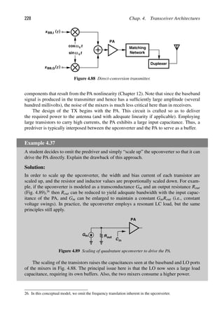
![Sec. 4.3. Transmitter Architectures 229
Among various TX architectures studied in this chapter, the direct-conversion approach
provides the most compact solution and a relatively “clean” output. That is, the output
spectrum contains only the desired signal around the carrier frequency (and its harmonics)
but no spurious components—an attribute similar to that of direct-conversion receivers.
Nonetheless, direct upconversion entails other issues that demand attention.
I/Q Mismatch We noted in Section 4.2 that I/Q mismatch in direct-conversion receivers
results in “cross-talk” between the quadrature baseband outputs or, equivalently, distortion
in the constellation. We expect a similar effect in the TX counterpart. For example, as
derived in Chapter 3, a phase mismatch of θ in the upconverter shifts the constellation
points of a QPSK signal to I 5 ± cos θ and Q 5 ±1 ± sin θ, just as observed for a
direct-conversion receiver. The results obtained in Chapter 3 can be extended to include
amplitude mismatch by writing
x(t) 5 α1(Ac 1 Ac) cos(ωct 1 θ) 1 α2Ac sin ωct (4.118)
5 α1(Ac 1 Ac) cos θ cos ωct 1 [α2Ac 2 α1(Ac 1 Ac) sin θ] sin ωct. (4.119)
Since α1 and α2 assume ±1 values, the normalized coefficients of cos ωct and sin ωct appear
as follows for the four points in the constellation:
β1 5 1
1 1
Ac
Ac
cos θ, β2 5 1 2
1 1
Ac
Ac
sin θ (4.120)
β1 5 1
1 1
Ac
Ac
cos θ, β2 5 21 2
1 1
Ac
Ac
sin θ (4.121)
β1 5 2
1 1
Ac
Ac
cos θ, β2 5 1 1
1 1
Ac
Ac
sin θ (4.122)
β1 5 2
1 1
Ac
Ac
cos θ, β2 5 21 1
1 1
Ac
Ac
sin θ. (4.123)
The reader is encouraged to compute the error vector magnitude (Chapter 3) of this
constellation.
Another approach to quantifying the I/Q mismatch in a transmitter involves apply-
ing two tones V0 cos ωint and V0 sin ωint to the I and Q inputs in Fig. 4.88 and
examining the output spectrum. In the ideal case, the output is simply given by
Vout 5 V0 cos ωint cos ωc t2 V0 sin ωint sin ωct 5 V0 cos(ωc 1 ωin)t. On the other hand, in
the presence of a (relative) gain mismatch of ε and a phase imbalance of θ, we have
Vout(t) 5 V0(1 1 ε) cos ωint cos(ωct 1 θ) 2 V0 sin ωint sin ωct (4.124)
5
V0
2
[(1 1 ε) cos θ 1 1] cos(ωct 1 ωin)t
2
V0
2
(1 1 ε) sin θ sin(ωc 1 ωin)t
1
V0
2
[(1 1 ε) cos θ 2 1] cos(ωc 2 ωin)t
2
V0
2
(1 1 ε) sin θ sin(ωc 2 ωin)t. (4.125)](https://image.slidesharecdn.com/rfmicroelectronicsrazavi-230814101614-71259b59/85/RF-MICROELECTRONICS_Razavi-pdf-254-320.jpg)
![230 Chap. 4. Transceiver Architectures
It follows that the power of the unwanted sideband at ωc 2ωin divided by that of the wanted
sideband at ωc 1 ωin is given by
P2
P1
5
[(1 1 ε) cos θ 2 1]2 1 (1 1 ε)2 sin2
θ
[(1 1 ε) cos θ 1 1]2 1 (1 1 ε)2 sin2
θ
(4.126)
5
(1 1 ε)2 2 2(1 1 ε) cos θ 1 1
(1 1 ε)2 1 2(1 1 ε) cos θ 1 1
, (4.127)
which is similar to the image-rejection ratio expression [Eq. (4.77)]. We may even call
the unwanted sideband the “image” of the wanted sideband with respect to the carrier fre-
quency. In practice, a P2/P1 of roughly 230 dB is sufficient to ensure negligible distortion
of the cancellation, but the exact requirement depends on the type of modulation.
Example 4.38
Compute the average power of Vout(t) in Eq. (4.125).
Solution:
We add P2 and P1 and multiply the result by V2
0 /4. If ε 1, then
V2
out(t) 5
V2
0
2
(1 1 ε). (4.128)
Interestingly, the output power is independent of the phase mismatch.
If the raw I/Q matching of circuits in a transmitter is inadequate, some means of cali-
bration can be employed. To this end, the gain and phase mismatch must first be measured
and subsequently corrected. Can we use the power of the unwanted sideband as a symptom
of the I/Q mismatch? Yes, but it is difficult to measure this power in the presence of the
large wanted sideband: the two sidebands are too close to each other to allow suppressing
the larger one by tens of decibels by means of a filter.
Let us now apply a single sinusoid to both inputs of the upconverter (Fig. 4.90). The
output emerges as
Vout3(t) 5 V0(1 1 ε) cos ωint cos(ωct 1 θ) 2 V0 cos ωint sin ωct (4.129)
5 V0 cos ωint(1 1 ε) cos θ cos ωct
2 V0 cos ωint[(1 1 ε) sin θ 1 1] sin ωct. (4.130)
It can be shown that the output contains two sidebands of equal amplitudes and carries an
average power equal to
V2
out3(t) 5 V2
0 [1 1 (1 1 ε) sin θ]. (4.131)](https://image.slidesharecdn.com/rfmicroelectronicsrazavi-230814101614-71259b59/85/RF-MICROELECTRONICS_Razavi-pdf-255-320.jpg)
![232 Chap. 4. Transceiver Architectures
That is,
V2
out1(t) 2 V2
out2(t) 5 V2
0 ε, (4.137)
suggesting that the gain mismatch can be adjusted so as to drive this difference to zero.
The measurement of V2
out3(t) and V2
out1(t) 2 V2
out2(t) in the above tests requires a rel-
atively high resolution. For example, a residual phase mismatch of θ 5 18 translates to
sin θ 5 1.75%, dictating a resolution of about 7–8 bits in the ADC that digitizes V2
out3(t)
in Eq. (4.131).
We should remark that dc offsets in the baseband may affect the accuracy of I/Q cali-
bration. As explained below, another effect, “carrier leakage,” may also require the removal
of dc offsets prior to I/Q calibration.
Carrier Leakage The analog baseband circuitry producing the quadrature signals in
the transmitter of Fig. 4.88 exhibits dc offsets, and so does the baseband port of each
upconversion mixer. Consequently, the output signal appears as
Vout(t) 5 [A(t) cos φ 1 VOS1] cos ωct 2 [A(t) sin φ 1 VOS2] sin ωct, (4.138)
where VOS1 and VOS2 denote the total dc offsets referred to the input port of the mixers.
The upconverter output therefore contains a fraction of the unmodulated carrier:
Vout(t) 5 A(t) cos(ωct 1 φ) 1 VOS1 cos ωct 2 VOS2 sin ωct. (4.139)
Called “carrier leakage,” and quantified as
Relative Carrier Leakage 5
V2
OS1 1 V2
OS2
A2(t)
, (4.140)
this phenomenon leads to two adverse effects. First, it distorts the signal constellation,
raising the error vector magnitude at the TX output. For example, if Vout(t) represents a
QPSK signal,
Vout(t) 5 α1(V0 1 VOS1) cos ωct 2 α2(V0 1 VOS2) sin ωct, (4.141)
and is applied to an ideal direct-conversion receiver, then the baseband quadrature outputs
suffer from dc offsets, i.e., horizontal and vertical shifts in the constellation (Fig. 4.92).
The second effect manifests itself if the output power of the transmitter must be varied
across a wide range by varying the amplitude of the baseband signals. For example, as
described in Chapter 3, CDMA mobiles must lower their transmitted power as they come
closer to the base station so as to avoid the near-far effect. Figure 4.93(a) conceptually
depicts the power control loop. The base station measures the power level received from the
mobile and, accordingly, requests the mobile to adjust its transmitted power. With a short
distance between the two, the mobile output power must be reduced to very low values,
yielding the spectrum shown in Fig. 4.93(b) in the presence of carrier leakage. In this case,
the carrier power dominates, making it difficult to measure the actual signal power. This](https://image.slidesharecdn.com/rfmicroelectronicsrazavi-230814101614-71259b59/85/RF-MICROELECTRONICS_Razavi-pdf-257-320.jpg)
![234 Chap. 4. Transceiver Architectures
t
cos
t
sinω c
ωc
Power
Detector
ADC
Register
DAC I
DAC Q
Baseband
Processor
Figure 4.94 Reduction of carrier leakage by baseband offset control.
Example 4.39
Is it possible to cancel the carrier leakage by means of a single DAC?
Solution:
No, it is not. Eq. (4.139) implies that no choice of VOS1 or VOS2 can force VOS1 cos ωct 2
VOS2 sin ωct to zero if the other remains finite.
How should the two DACs be adjusted so that the loop in Fig. 4.94 converges? An
adaptive loop such as the least mean square (LMS) algorithm can perform this task. Alter-
natively, an “exhaustive” search can arrive at the optimum settings; e.g., for 8-bit DACs,
only 256 3 256 possible combinations exist, and the system can try all to determine which
combination yields the lowest leakage at the output. In this procedure, the system begins
with, say, zero settings for both DACs, measures the carrier leakage, memorizes this value,
increments one DAC by 1 LSB, measures the leakage again, and compares the result with
the previous value. The new settings replace the previous ones if the new leakage is lower.
Mixer Linearity Unlike downconversion mixers in a receiver, upconversion mixers in
a transmitter sense no interferers. However, excessive nonlinearity in the baseband port
of upconversion mixers can corrupt the signal or raise the adjacent channel power (Chap-
ter 3). As an example, consider the GMSK signal expressed by Eq. (4.112) and suppose
the baseband I/Q inputs experience a nonlinearity given by α1x 1 α3x3. The upconverted
signal assumes the form [15]
Vout(t) 5 (α1A cos φ 1 α3A3
cos3
φ) cos ωct 2 (α1A sin φ 1 α3A3
sin3
φ) sin ωct (4.142)
5
α1A 1
3
4
α3A3
cos(ωct 1 φ) 1
α3A3
4
cos(ωct 2 3φ). (4.143)](https://image.slidesharecdn.com/rfmicroelectronicsrazavi-230814101614-71259b59/85/RF-MICROELECTRONICS_Razavi-pdf-259-320.jpg)
![Sec. 4.3. Transmitter Architectures 235
The second term also represents a GMSK signal but with a threefold modulation index,
thereby occupying a larger bandwidth. Simulations indicate that this effect becomes neg-
ligible if the baseband port of the mixers experiences a nonlinearity less than 1% for the
specified baseband swings [15].
For variable-envelope signals, A3(t) appears in both terms of Eq. (4.143), exacerbating
the effect. The required mixer linearity is typically determined by simulations. However, in
most cases (i.e., in a good design), as the baseband signal swings increase, the PA output
begins to compress before the mixer nonlinearity manifests itself. This is explained below.
TX Linearity The linearity of transmitters must be chosen according to the spectral
regrowth (adjacent channel power) requirements and/or the tolerable distortion of the sig-
nal to be transmitted. As mentioned in Chapter 3, both of these effects become critical for
variable-envelope modulation schemes. We defer the former to Chapter 12 and deal with
the latter here.
The distortion of a variable-envelope signal is typically characterized by the compres-
sion that it experiences. As shown in Fig. 4.95, the signal is subjected to a nonlinear
characteristic in simulations and it is determined how close its level can come to the
1-dB compression point while the degradation in the constellation or the bit error rate is
negligible. For example, the average power of the 64-QAM OFDM signal in 802.11a must
remain about 8 dB below P1dB of a given circuit. We say the circuit must operate at “8-dB
back-off.” In other words, if a peak swing of V0 places the circuit at the 1-dB compression
point, then the average signal swing must not exceed V0/2.51.
In a TX chain, the signal may experience compression in any of the stages. Consider
the example depicted in Fig. 4.96, where the signal levels (in dB) along the chain are also
shown. Since the largest voltage swing occurs at the output of the PA, this stage dominates
the compression of the TX; i.e., in a good design, the preceding stages must remain well
below compression as the PA output approaches P1dB. To so ensure, we must maximize the
gain of the PA and minimize the output swing of the predriver and the stages preceding it.
This requirement places additional burden on the PA design (Chapters 12 and 13).
V0
1−dB Compression
Point
t
out
V
in
V
Figure 4.95 Variable-envelope signal applied to a compressive system.](https://image.slidesharecdn.com/rfmicroelectronicsrazavi-230814101614-71259b59/85/RF-MICROELECTRONICS_Razavi-pdf-260-320.jpg)
![Sec. 4.3. Transmitter Architectures 237
Example 4.40 (Continued)
where the factor 1/1.12 accounts for the 1-dB gain reduction. It follows that
A1dB,out 5
0.34|α1β1|
√
|β1α1|
β1α3 1 β3α3
1
. (4.148)
Oscillator Pulling While the issues described above apply to most transmitter archi-
tectures, another one becomes particularly critical in direct-conversion topologies. As
illustrated in Fig. 4.97(a), the PA output exhibits very large swings (20 Vpp for 1 W
delivered to a 50- load), which couple to various parts of the system through the silicon
substrate, package parasitics, and traces on the printed-circuit board. Thus, it is likely that
an appreciable fraction of the PA output couples to the local oscillator. Even if the PA is off-
chip, the PA driver may still pull the LO. Note that the center frequency of the PA output
spectrum is equal to ωLO in direct-conversion transmitters.
Let us consider a “sliver” of the output spectrum centered at ωLO 1 ω and model it by
an impulse of equal energy [Fig. 4.97(b)]. We therefore inquire what happens if a sinusoid
at a frequency of ω1 5 ωLO 1 ω is “injected” into an oscillator operating at a frequency
of ωLO, where ω ωLO. Called “injection pulling,” this phenomenon has been studied
extensively [16, 17] and is analyzed in Chapter 8. In such a condition, the output phase
of the oscillator, φout, is modulated periodically. In fact, as depicted in Fig. 4.98(a), φout
remains around 908 (with respect to the input phase) for part of the period, subsequently
experiencing a rapid 3608 rotation. The input and output waveforms therefore appear as in
Fig. 4.98(b). It can be proved that the output spectrum is heavily asymmetric [Fig. 4.98(c)],
with most of the impulses located away from the input frequency, ωinj (5ωLO 1 ω). Note
that the spacing between the impulses is equal to the frequency of the phase variation in
Fig. 4.98(a) and not equal to ω.28
PA
I
Q
ω
LO
LO
ωLO
Δω
ω
LO
ω
LO
Δω
ω
(a) (b)
φ out
Figure 4.97 (a) Injection pulling of LO by PA in a direct-conversion TX, (b) conceptual illustration
of injection into an oscillator.
28. Pulling can also occur if the injected signal frequency is close to a harmonic of the oscillator frequency,
e.g., in the vicinity of 2ωLO. We call this effect “superharmonic pulling.”](https://image.slidesharecdn.com/rfmicroelectronicsrazavi-230814101614-71259b59/85/RF-MICROELECTRONICS_Razavi-pdf-262-320.jpg)
![238 Chap. 4. Transceiver Architectures
ω
ωinj
ω
+
ωinj b
ω
ωinj b
+ 2
Output
Spectrum
(c)
ω
ωinj b
+ 3
t
2
π
+
π
+
π
−
out
V
in
V
t
φout
360
Rotation
(a)
(b)
Figure 4.98 (a) Behavior of LO output phase in the presence of injection pulling, (b) cycle slips in
time domain, (c) resulting spectrum.
At what output power level does injection pulling become significant? The answer
depends on several factors: (1) the internal voltage and current swings of the LO (the larger
they are, the less is the effect of pulling); (2) the Q of the tank used in the oscillator;
(3) whether the PA output is differential, in which case its coupling to the LO is 30–40 dB
lower than if it is single-ended;29
(4) how much the feedback loop controlling the LO (the
synthesizer) counteracts the pulling [17]; (5) the symmetry of the layout and the type of
packaging. Nonetheless, for typical designs, as the PA output exceeds 0 dBm, injection
pulling may prove serious.
In order to avoid injection pulling, the PA output frequency and the oscillator frequency
must be made sufficiently different (e.g., by more than 20%), an impossible task in the
architecture of Fig. 4.97. This principle has led to a number of transmitter architectures and
frequency plans that are described below.
Noise in RX Band As explained in Chapter 3, some standards (e.g., GSM) specify the
maximum noise that a TX can transmit in the RX band. In a direct-conversion transmitter,
the baseband circuits, the upconverter, and the PA may create significant noise in the RX
band. To resolve this issue, “offset-PLL” transmitters can be used (Chapter 9).
4.3.3 Modern Direct-Conversion Transmitters
Most of today’s direct-conversion transmitters avoid an oscillator frequency equal to the PA
output frequency. To avoid confusion, we call the former the LO frequency, ωLO, and the
29. This is true only if the differential PA incorporates “single-ended” inductors rather than one symmetric
inductor (Chapter 7).](https://image.slidesharecdn.com/rfmicroelectronicsrazavi-230814101614-71259b59/85/RF-MICROELECTRONICS_Razavi-pdf-263-320.jpg)
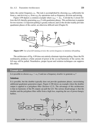
![240 Chap. 4. Transceiver Architectures
The principal drawback of the architecture of Fig. 4.99 stems from the speed required
of the divider. Operating at twice the carrier frequency, the divider may become the speed
bottleneck of the entire transceiver. (We deal with divider design in Chapter 10.) Nev-
ertheless, as seen in the following discussion, other transmitter architectures suffer from
more serious drawbacks. Thus, even a substantial effort on divider design to enable this
architecture is well justified.
Another approach to deriving frequencies is through the use of mixing. For example,
mixing the outputs of two oscillators operating at ω1 and ω2 can yield ω1 1 ω2 or ω1 2 ω2.
Nonetheless, as with the receivers studied in Section 4.2, it is desirable to employ a sin-
gle oscillator and utilize division to obtain subharmonics. To this end, let us consider the
arrangement shown in Fig. 4.101(a), where the oscillator frequency is divided by 2 and the
two outputs are mixed. The result contains components at ω1±ω1/2 with equal magnitudes.
We may call one the “image” of the other with respect to ω1.
LO
ω
PA
ω
I Q
2
1
ω
2
1
ω
ω
2
1 ω
2
1
3
Quadrature
Upconverter
)
(t
xBB,I
(t
xBB,Q
ω
ω
2
1 ω
2
1
3
LO
ω
2
1 ω
2
3
(a) (b)
1
)
Figure 4.101 (a) Mixing of an LO output with half of its frequency, (b) effect of two sidebands on
transmitter output.
Can both components be retained? In a transmitter using such an LO waveform, the
upconverter output would contain, with equal power, the signal spectrum at both carrier
frequencies [Fig. 4.101(b)]. Thus, half of the power delivered to the antenna is wasted.
Furthermore, the power transmitted at the unwanted carrier frequency corrupts communi-
cation in other channels or bands. One component (e.g., that at ω1/2) must therefore be
suppressed.
It is difficult to remove the unwanted carrier by means of filtering because the two
frequencies differ by only a factor of 3. For example, in Problem 4.24 we show that a
second-order LC filter resonating at 3ω1/2 attenuates the component at ω1/2 by a factor of
8Q/3. For a Q in the range of 5 to 10, this attenuation amounts to 25 to 30 dB, sufficient for
minimizing the waste of power in the unwanted sideband but inadequate for avoiding cor-
ruption of other channels. The other issue is that the output in Fig. 4.101(a) is not available
in quadrature form.
An alternative method of suppressing the unwanted sideband incorporates “single-
sideband” (SSB) mixing. Based on the trigonometric identity cos ω1t cos ω2t 2 sin ω1t
sin ω2t 5 cos(ω1 1 ω2)t and illustrated in Fig. 4.102(a), SSB mixing involves multiply-
ing the quadrature phases of ω1 and ω2 and subtracting the results—just as realized by the
quadrature upconverter of Fig. 4.88. We denote an SSB mixer by the abbreviated symbol](https://image.slidesharecdn.com/rfmicroelectronicsrazavi-230814101614-71259b59/85/RF-MICROELECTRONICS_Razavi-pdf-265-320.jpg)
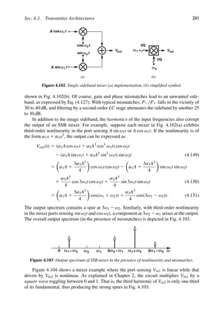
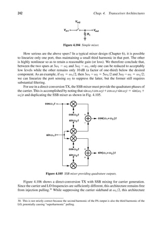
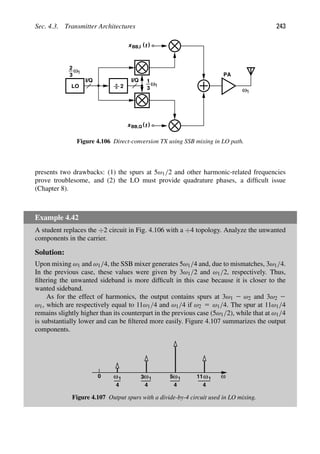
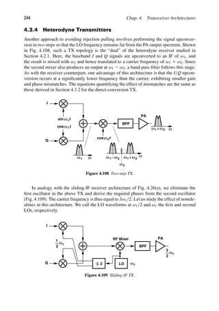
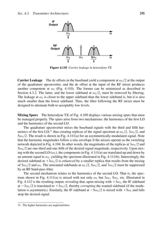
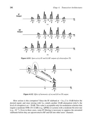
![Sec. 4.3. Transmitter Architectures 247
LO
PA
I
Q
cos
RF SSB Mixer
2
)
(t
xBB,I = )
(t
A θ
)
(t
x = )
(t
A θ
sin
BB,Q
ω1
3
2
ω1
Figure 4.113 Use of baseband quadrature SSB mixing and IF SSB mixing to reduce the unwanted
component.
Example 4.43
Compare the spurious behavior of the TX architectures shown in Figs. 4.106 and 4.109.
Solution:
In the direct-conversion TX of Fig. 4.106, the primary spur appears at 5ω1/2 , and no self-
corruption similar to that illustrated in Fig. 4.112 exists. The heterodyne topology, on the
other hand, suffers from more spurs.
The unwanted sideband at ω1 2 ω1/2 produced by the RF mixer in Fig. 4.109 can
be greatly suppressed through the use of SSB mixing. To this end, the IF signal must be
generated in quadrature form. Figure 4.113 shows such a topology [15, 18], where two
quadrature upconverters provide the quadrature components of the IF signal:
xIF,I(t) 5 A(t) cos θ cos
ω1t
2
2 A(t) sin θ sin
ω1t
2
(4.152)
5 A(t) cos
ω1t
2
1 θ
(4.153)](https://image.slidesharecdn.com/rfmicroelectronicsrazavi-230814101614-71259b59/85/RF-MICROELECTRONICS_Razavi-pdf-272-320.jpg)
![248 Chap. 4. Transceiver Architectures
xIF,Q(t) 5 A(t) cos θ sin
ω1t
2
1 A(t) sin θ cos
ω1t
2
(4.154)
5 A(t) sin
ω1t
2
1 θ
. (4.155)
The RF SSB mixer then translates the result to ω1 1 ω1/2. The reader is encouraged to
study the mixing spurs in this architecture.
While attenuating the sideband at ω1 2ω1/2, the architecture of Fig. 4.113 suffers from
three drawbacks: (1) the oscillator must provide quadrature outputs, a difficult issue (Chap-
ter 8), (2) the circuit employs twice as many mixers as those in the original architecture
(Fig. 4.109), and (3) the loading seen by the ÷2 circuit is doubled. The first issue can be
alleviated by operating the oscillator at 2ω1 and following it with a ÷2 stage, but such a
design is only slightly simpler than the direct-conversion architecture of Fig. 4.106.
Our study of the heterodyne sliding-IF TX has thus far assumed that the first LO fre-
quency is half of the second LO frequency. It is possible to replace the ÷2 circuit with a
÷4 stage so as to produce the IF signal at ω1/4 and the RF output at ω1 1 ω1/4 5 5ω1/4
[19]. We study the spurious effects in such an architecture in Problem 4.25.
4.3.5 Other TX Architectures
In addition to the TX architectures described above, several others find usage in some
applications. These include “offset PLL” topologies, “in-loop modulation” systems, and
“polar modulation” transmitters. We study the first two in Chapter 10 and the last in
Chapter 12.
4.4 OOK TRANSCEIVERS
“On-off keying” (OOK) modulation is a special case of ASK where the carrier amplitude
is switched between zero and maximum. Transceivers employing OOK lend themselves to
a compact, low-power implementation and merit some study here. Figure 4.114 illustrates
two TX topologies. In Fig. 4.114(a), the LO is directly turned on and off by the binary
baseband data. If the LO swings are large enough, the PA also experiences relatively com-
plete switching and delivers an OOK waveform to the antenna. In contrast to the transmitter
architectures studied in the previous sections, OOK does not require quadrature baseband
or LO waveforms or a quadrature upconverter. Of course, it is also less bandwidth-efficient
as unshaped binary pulses modulated on one phase of the carrier occupy a wide spectrum.
LO
PA
LO
PA
(a) (b)
Figure 4.114 OOK TX with (a) direct LO switching (b) PA switching.](https://image.slidesharecdn.com/rfmicroelectronicsrazavi-230814101614-71259b59/85/RF-MICROELECTRONICS_Razavi-pdf-273-320.jpg)
![References 249
LNA
Envelope
Detector
Figure 4.115 OOK receiver.
Nonetheless, the simplicity of the architecture makes it attractive for low-cost, low-power
applications.
The principal issue in the TX of Fig. 4.114(a) is that the LO cannot be easily controlled
by a phase-locked loop (Chapter 9). The TX of Fig. 4.114(b), on the other hand, keeps the
LO on and directly switches the PA. We study the injection-pulling properties of the two
architectures in Problem 4.29.
OOK receivers are also simple and compact. As shown in Fig. 4.115, an LNA followed
by an envelope detector can recover the binary data, with no need for an LO. Of course,
such a receiver has little tolerance of interferers.
REFERENCES
[1] B. Razavi et al., “Multiband UWB Transceivers,” Proc. CICC, pp. 141–148, Sept 2005.
[2] B. Razavi, “Design Considerations for Direct-Conversion Receivers,” IEEE Trans. Circuits
and Systems, vol. 44, pp. 428–435, June 1997.
[3] A. A. Abidi, “Direct-conversion Radio Transceivers for Digital Communications,” IEEE
Journal of Solid-State Circuits, vol. 30, pp. 1399–1410, Dec. 1995.
[4] R. Hartley, “Modulation System,” US Patent 1,666,206, April 1928.
[5] D. K. Weaver, “A Third Method of Generation and Detection of Single-Sideband Signals,”
Proc. IRE, vol. 44, pp. 1703–1705, Dec. 1956.
[6] J. Rudell et al., “A 1.9-GHz Wideband IF Double Conversion CMOS Receiver for Cordless
Telephone Applications,” IEEE Journal of Solid-State Circuits, vol. 32, pp. 2071–2088, Dec.
1997.
[7] L. Der and B. Razavi, “A 2-GHz CMOS Image-Reject Receiver with LMS Calibration,” IEEE
Journal of Solid-State Circuits, vol. 38, pp. 167–175, Feb. 2003.
[8] M. Gingell, “Single-Sideband Modulation Using Sequence Asymmetric Polyphase Net-
works,” Elec. Comm., vol. 48, pp. 21–25, 1973.
[9] S. Lerstaveesin and B. S. Song, “A Complex Image Rejection Circuit with Sign Detection
Only,” IEEE J. Solid-State Circuits, vol. 41, pp. 2693–2702, Dec. 2006.
[10] J. Crols and M. S. J. Steyaert, “A Single-Chip 900-MHz CMOS Receiver Front End with a
High-Perfromance Low-IF Topology,” IEEE J. Solid-State Circuits, vol. 30, pp. 1483–1492,
Dec. 1995.
[11] F. Behbahani et al., “CMOS Mixers and Polyphase Filters for Large Image Rejection,” IEEE
J. Solid-State Circuits, vol. 36, pp. 873–887, June 2001.
[12] J. Crols and M. S. J. Steyaert, “Low-IF Topologies for High-Performance Analog Front Ends
of Fully Integrated Receivers,” IEEE Tran. Circuits and Sys., II, vol. 45, pp. 269–282, March
1998.
[13] K. Feher, Wireless Digital Communications, New Jersey: Prentice-Hall, 1995.
[14] R. Steele, Ed., Mobile Radio Communications, New Jersey: IEEE Press, 1992.
[15] B. Razavi, “A 900-MHz/1.8-GHz CMOS Transmitter for Dual-Band Applications,” IEEE
Journal of Solid-State Circuits, vol. 34, pp. 573–579, May 1999.](https://image.slidesharecdn.com/rfmicroelectronicsrazavi-230814101614-71259b59/85/RF-MICROELECTRONICS_Razavi-pdf-274-320.jpg)
![250 Chap. 4. Transceiver Architectures
[16] R. Adler, “A Study of Locking Phenomena in Oscillators,” Proc. of the IEEE, vol. 61, No. 10,
pp. 1380–1385, Oct. 1973.
[17] B. Razavi, “A Study of Injection Locking and Pulling in Oscillators,” IEEE J. of Solid-State
Circuits, vol. 39, pp. 1415–1424, Sep. 2004.
[18] M. Zargari et al., “A 5-GHz CMOS Transceiver for IEEE 802.11a Wireless LAN Systems,”
IEEE J. of Solid-State Circuits, vol. 37, pp. 1688–1694, Dec. 2002.
[19] S. A. Sanielevici et al., “A 900-MHz Transceiver Chipset for Two-Way Paging Applications,”
IEEE J. of Solid-State Circuits, vol. 33, pp. 2160–2168, Dec. 1998.
[20] M. Conta, private communication, Feb. 2011.
[21] B. Razavi, “A 5.2-GHz CMOS Receiver with 62-dB Image Rejection,” IEEE Journal of Solid-
State Circuits, vol. 36, pp. 810–815, May 2001.
[22] A. Parsa and B. Razavi, “A New Transceiver Architecture for the 60-GHz Band,” IEEE
Journal of Solid-State Circuits, vol. 44, pp. 751–762, Mar. 2009.
PROBLEMS
4.1. For the sliding-IF architecture of Fig. 4.26(a), assume the ÷2 circuit is replaced with
a ÷4 circuit.
(a) Determine the required LO frequency range and steps.
(b) Determine the image frequency range.
4.2. Since the image band of the sliding-IF receiver of Fig. 4.26(a) is narrower than the
signal band, is it possible to design an 11g receiver whose image is confined to the
GPS band? Explain your reasoning.
4.3. A sliding-IF receiver with fLO 5 (2/3)fin is designed for the 11g band. Determine
some of the mixing spurs that result from the harmonics of the first LO and the
second LO. Assume the second IF is zero.
4.4. Consider the 11g sliding-IF receiver shown in Fig. 4.116.
(a) Determine the required LO frequency range.
(b) Determine the image frequency range.
(c) Is this architecture preferable to that in Fig. 4.26(a)? Why?
Qout
Iout
LNA
I Q
fin
LO
2
Figure 4.116 Sliding-IF RX for 11g.](https://image.slidesharecdn.com/rfmicroelectronicsrazavi-230814101614-71259b59/85/RF-MICROELECTRONICS_Razavi-pdf-275-320.jpg)
![Problems 251
4.5. Determine some of the mixing spurs in the architecture of Fig. 4.116.
4.6. The sliding-IF architecture shown in Fig. 4.117 is designed for the 11a band.
(a) Determine the image band.
(b) Determine the interferer frequencies that can appear in the output baseband as a
result of mixing with the third harmonic of the first LO or the third harmonic of
the second LO.
( (
t
xBB,I
( (
t
xBB,Q
LNA
BPF
LO
f
1
LO1
LO2,Q
LO2,I fLO1
fin
8 8
Figure 4.117 Sliding-IF RX for 11a.
4.7. Figure 4.118 shows a “half-RF” architecture, where fLO 5 f 2 in/2 [21, 22].
(a) Assume the RF input is an asymmetrically-modulated signal. Sketch the spectra
at the first and second IFs if the mixers are ideal multipliers.
(b) Repeat part (a) but assuming that the RF mixer also multiplies the RF signal by
the third harmonic of the LO.
(c) The flicker noise of the LNA may be critical here. Explain why.
Qout
Iout
LNA
I Q
fin
LO
Figure 4.118 Half-RF RX.
4.8. Suppose an AM signal, A(t) cos ωct, is applied to a single mixer driven by an LO.
(a) If the LO waveform is given by cos ωct, determine the baseband signal.
(b) If the LO waveform is given by sin ωct, what happens? Why does this indicate
the need for quadrature downconversion?](https://image.slidesharecdn.com/rfmicroelectronicsrazavi-230814101614-71259b59/85/RF-MICROELECTRONICS_Razavi-pdf-276-320.jpg)
![252 Chap. 4. Transceiver Architectures
4.9. In this problem we wish to study an interesting effect that arises from LO leakage
in direct-conversion receivers [20]. Consider the LO leakage in a direct-conversion
receiver, V0 cos ωLOt. Suppose this leakage is added to an amplitude-modulated
interferer, Vint(t) cos ωintt, and the result experiences third-order nonlinearity in the
LNA (or downconversion mixer).
(a) Determine the components near the carrier at the LNA output.
(b) Determine the resulting baseband components and whether they corrupt the
desired signal.
4.10. In Example 4.24, how much gain must precede the given noise spectrum so that the
penalty remains below 1 dB?
4.11. In Example 4.24, what flicker noise corner frequency is necessary if the penalty must
remain below 1 dB?
4.12. An ASK waveform is applied to a direct-conversion receiver. Plot the baseband I and
Q waveforms.
4.13. Does the quadrature mixing of Fig. 4.59(a) perform a Hilbert transform if the
upconverted outputs at ωc 1 ωLO are considered?
4.14. Repeat the analysis in Fig. 4.59 if ωIF ωc.
4.15. Does the Hartley architecture cancel the image if the IF low-pass filters are replaced
with high-pass filters and the upconverted components are considered?
4.16. In the architecture of Fig. 4.64, assume the two resistors have a mismatch of R.
Compute the IRR.
4.17. Prove that the IRR of the Hartley architecture is given by (ωIF/ ω)2 at an
intermediate frequency of ωIF 1 ω if ωIF 5 (R1C1)21.
4.18. Considering only the thermal noise of the resistors in Fig. 4.64 and assuming a volt-
age gain of A1 for each mixer, determine the noise figure of the receiver with respect
to a source impedance of RD.
4.19. In the Weaver architecture of Fig. 4.67, both quadrature downconversions were per-
formed with low-side injection. Study the other three combinations of high-side and
low-side injection with the aid of signal spectra at nodes A-F.
4.20. Figure 4.119 shows three variants of the Hartley architecture. Explain which one(s)
can reject the image.
4.21. If sin ωLOt and cos ωLOt in the Hartley architecture are swapped, does the RX still
reject the image?
4.22. Repeat the above problem for the first or second LO in a Weaver architecture.
4.23. Using Eq. (4.96), compute the IRR of the receiver shown in Fig. 4.77(b) at an IF of
ω 1 ω.
4.24. Assume a second-order parallel RLC tank is excited by a current source containing
a component at ω0 and another at 3ω0. Prove that, if the tank resonates at 3ω0, then
the first harmonic is attenuated by approximately a factor of 8Q/3 with respect to the
third harmonic.](https://image.slidesharecdn.com/rfmicroelectronicsrazavi-230814101614-71259b59/85/RF-MICROELECTRONICS_Razavi-pdf-277-320.jpg)
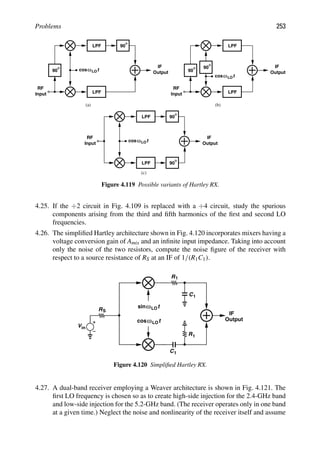
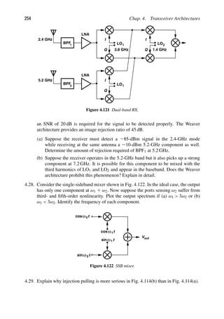
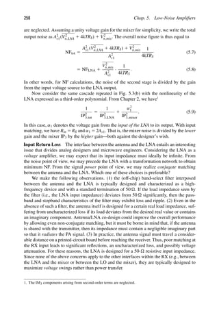
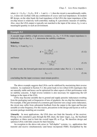
![Sec. 5.1. General Considerations 261
Duplexer
LNA
PA
RX
TX
1
2
3
Leakage
ω
Transmitted
Signal
Transmit
Band Band
Receive
+30 dBm
ω
Signal
Transmit
Band Band
Receive
−20 dBm
Received
Figure 5.5 TX leakage to RX in a full-duplex system.
CDMA systems studied in Chapter 3, full-duplex operation must deal with the leakage
of the strong transmitted signal to the receiver. To understand this issue, let us consider the
front end shown in Fig. 5.5, where a duplexer separates the TX and RX bands. Modeling
the duplexer as a three-port network, we note that S31 and S21 represent the losses in the RX
and TX paths, respectively, and are about 1 to 2 dB. Unfortunately, leakages through the fil-
ter and the package yield a finite isolation between ports 2 and 3, as characterized by an S32
of about 250 dB. In other words, if the PA produces an average output power of 130 dBm
(1 W), then the LNA experiences a signal level of 220 dBm in the TX band while sensing
a much smaller received signal. Since the TX signal exhibits a variable envelope, its peak
level may be about 2 dB higher. Thus, the receiver must remain uncompressed for an input
level of 218 dBm. We must therefore choose a P1dB of about 215 dBm to allow some
margin.
Such a value for P1dB may prove difficult to realize in a receiver. With an LNA gain of
15 to 20 dB, an input of 215 dBm yields an output of 0 to 15 dBm (632 to 1124 mVpp),
possibly compressing the LNA at its output. The LNA linearity is therefore critical. Simi-
larly, the 1-dB compression point of the downconversion mixer(s) must reach 0 to 15 dBm.
(The corresponding mixer IP3 is roughly 110 to 115 dBm.) Thus, the mixer design also
becomes challenging. For this reason, some CDMA receivers interpose an off-chip filter
between the LNA and the mixer(s) so as to remove the TX leakage [1].
The linearity of the LNA also becomes critical in wideband receivers that may sense a
large number of strong interferers. Examples include “ultra-wideband” (UBW), “software-
defined,” and “cognitive” radios.
Bandwidth The LNA must provide a relatively flat response for the frequency range of
interest, preferably with less than 1 dB of gain variation. The LNA 23-dB bandwidth must
therefore be substantially larger than the actual band so that the roll-off at the edges remains
below 1 dB.](https://image.slidesharecdn.com/rfmicroelectronicsrazavi-230814101614-71259b59/85/RF-MICROELECTRONICS_Razavi-pdf-286-320.jpg)
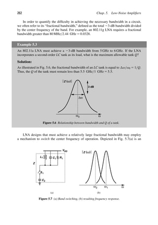
![Sec. 5.2. Problem of Input Matching 263
example, where an additional capacitor, C2, can be switched into the tank, thereby chang-
ing the center frequency from ω1 5 1/
√
L1C1 to ω2 5 1/
√
L1(C1 1 C2) [Fig. 5.7(b)]. We
return to this concept in Section 5.5.
Power Dissipation The LNA typically exhibits a direct trade-off among noise, linearity,
and power dissipation. Nonetheless, in most receiver designs, the LNA consumes only
a small fraction of the overall power. In other words, the circuit’s noise figure generally
proves much more critical than its power dissipation.
5.2 PROBLEM OF INPUT MATCHING
As explained in Section 5.1, LNAs are typically designed to provide a 50- input resistance
and negligible input reactance. This requirement limits the choice of LNA topologies. In
other words, we cannot begin with an arbitrary configuration, design it for a certain noise
figure and gain, and then decide how to create input matching.
Let us first consider the simple common-source stage shown in Fig. 5.8, where CF
represents the gate-drain overlap capacitance. At very low frequencies, RD is much smaller
than the impedances of CF and CL and the input impedance is roughly equal to [(CGS 1
CF)s]21. At very high frequencies, CF shorts the gate and drain terminals of M1, yielding
an input resistance equal to RD||(1/gm). More generally, the reader can prove that the real
and imaginary parts of the input admittance are, respectively, equal to
Re{Yin} 5 RDCFω2 CF 1 gmRD(CL 1 CF)
R2
D(CL 1 CF)2ω2 1 1
(5.15)
Im{Yin} 5 CFω
R2
DCL(CL 1 CF)ω2 1 1 1 gmRD
R2
D(CL 1 CF)2ω2 1 1
. (5.16)
Is it possible to select the circuit parameters so as to obtain Re{Yin} 5 1/(50 )? For exam-
ple, if CF 5 10 fF, CL 5 30 fF, gmRD 5 4, and RD 5 100 , then Re{Yin} 5 (7.8 k)21 at
5 GHz, far from (50 )21. This is because CF introduces little feedback at this frequency.
M 1
RD
VDD
out
V
in
V
CF
CGS
CL
in
Y
Figure 5.8 Input admittance of a CS stage.](https://image.slidesharecdn.com/rfmicroelectronicsrazavi-230814101614-71259b59/85/RF-MICROELECTRONICS_Razavi-pdf-288-320.jpg)
![264 Chap. 5. Low-Noise Amplifiers
Example 5.4
Why did we compute the input admittance rather than the input impedance for the circuit
of Fig. 5.8.
Solution:
The choice of one over the other is somewhat arbitrary. In some circuits, it is simpler to
compute Yin. Also, if the input capacitance is cancelled by a parallel inductor, then Im{Yin}
is more relevant. Similarly, a series inductor would cancel Im{Zin}. We return to these
concepts later in this chapter.
Can we employ simple resistive termination at the input? Illustrated in Fig. 5.9(a),
such a topology is designed in three steps: (1) M1 and RD provide the required noise figure
and gain, (2) RP is placed in parallel with the input to provide Re{Zin} 5 50 , and (3)
an inductor is interposed between RS and the input to cancel Im{Zin}. Unfortunately, as
explained in Chapter 2, the termination resistor itself yields a noise figure of 11RS/RP. To
calculate the noise figure at low frequencies, we can utilize Friis’ equation4
or simply treat
the entire LNA as one circuit and, from Fig. 5.9(b), express the total output noise as
V2
n,out 5 4kT(RS||RP)(gmRD)2
1 4kTγ gmR2
D 1 4kTRD, (5.17)
where channel-length modulation is neglected. Since the voltage gain from Vin to Vout in
Fig. 5.9(a) is equal to 2[RP/(RP 1 RS)]gmRD, the noise figure is given by
NF 5 1 1
RS
RP
1
γ RS
gm(RS||RP)2
1
RS
g2
m(RS||RP)2RD
. (5.18)
For RP ≈ RS, the NF exceeds 3 dB—perhaps substantially.
The key point in the foregoing study is that the LNA must provide a 50- input resis-
tance without the thermal noise of a physical 50- resistor. This becomes possible with the
aid of active devices.
M 1
RD
VDD
out
V
RP
L1
Vin
RS
M 1
RD
VDD
RS RP
RS RP
V
2
n,out
kT
4 ( )
kT
4 γ gm
(a) (b)
Figure 5.9 (a) Use of resistive termination for matching, (b) simplified circuit.
4. That is, consider RP as one stage and the CS amplifier as another.](https://image.slidesharecdn.com/rfmicroelectronicsrazavi-230814101614-71259b59/85/RF-MICROELECTRONICS_Razavi-pdf-289-320.jpg)
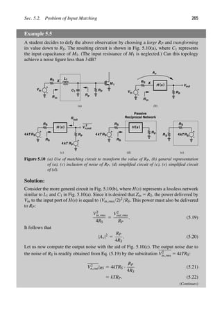
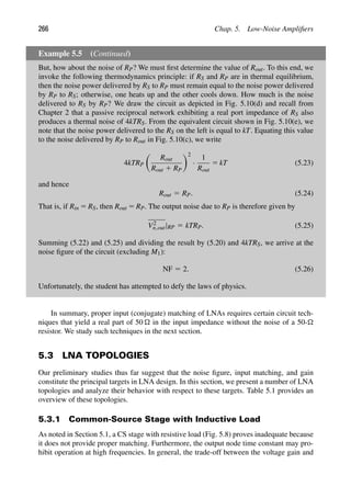
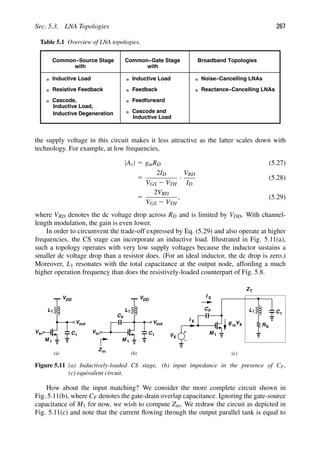
![268 Chap. 5. Low-Noise Amplifiers
IX 2gmVX. In this case, the inductor loss is modeled by a series resistance, RS, because this
resistance varies much less with frequency than the equivalent parallel resistance does.5
The tank impedance is given by
ZT 5
L1s 1 RS
L1C1s2 1 RSC1s 1 1
, (5.30)
and the tank voltage by (IX 2 gmVX)ZT. Adding the voltage drop across CF to the tank
voltage, we have
VX 5
IX
CFs
1 (IX 2 gmVX)ZT. (5.31)
Substitution of ZT from (5.30) gives
Zin(s) 5
VX
IX
5
L1(C1 1 CF)s2 1 RS(C1 1 CF)s 1 1
[L1C1s2 1 (RSC1 1 gmL1)s 1 1 1 gmRS]CFs
. (5.32)
For s 5 jω,
Zin(jω) 5
1 2 L1(C1 1 CF)ω2 1 jRS(C1 1 CF)ω
[2(RSC1 1 gmL1)ω 1 j(gmRS 2 L1C1ω2 1 1)]CFω
. (5.33)
Since the real part of a complex fraction (a 1 jb)/(c 1 jd) is equal to (ac 1 bd)/(c2 1 d2),
we have
Re{Zin} 5
[1 2 L1(C1 1 CF)ω2][2(RSC1 1 gmL1)ω] 1 RS(C1 1 CF)(gmRS 2 L1C1ω2 1 1)ω2
D
,
(5.34)
where D is a positive quantity. It is thus possible to select the values so as to obtain
Re{Zin} 5 50 .
While providing the possibility of Re{Zin} 5 50 at the frequency of interest, the
feedback capacitance in Fig. 5.11(b) gives rise to a negative input resistance at other
frequencies, potentially causing instability. To investigate this point, let us rewrite
Eq. (5.34) as
Re{Zin} 5
gmL2
1(C1 1 CF)ω2 1 RS(1 1 gmRS)(C1 1 CF) 2 (RSC1 1 gmL1)
D
ω. (5.35)
We note that the numerator falls to zero at a frequency given by
ω2
1 5
RSC1 1 gmL1 2 (1 1 gmRS)RS(C1 1 CF)
gmL2
1(C1 1 CF)
. (5.36)
5. For example, if RS simply represents the low-frequency resistance of the wire, its value remains con-
stant and Q 5 Lω/RS rises linearly with frequency. For a parallel resistance, RP, to allow such a behavior
for Q 5 RP/(Lω), the resistance must rise in proprotion to ω2 rather than remain constant.](https://image.slidesharecdn.com/rfmicroelectronicsrazavi-230814101614-71259b59/85/RF-MICROELECTRONICS_Razavi-pdf-293-320.jpg)
![Sec. 5.3. LNA Topologies 269
Thus, at this frequency (if it exists), Re{Zin} changes sign. For example, if CF 5 10 fF,
C1 5 30 fF, gm 5 (20 )21, L1 5 5 nH, and RS 5 20 , then gmL1 dominates in the
numerator, yielding ω2
1 ≈ [L1(C1 1 CF)]21 and hence ω1 ≈ 2π 3 (11.3 GHz).
It is possible to “neutralize” the effect of CF in some frequency range through the use
of parallel resonance (Fig. 5.12), but, since CF is relatively small, LF must assume a large
value, thereby introducing significant parasitic capacitances at the input and output (and
even between the input and output) and degrading the performance. For these reasons, this
topology is rarely used in modern RF design.
M 1
VDD
out
V
in
V
CF
C1
L
L1
F
Figure 5.12 Neutralization of CF by LF.
5.3.2 Common-Source Stage with Resistive Feedback
If the frequency of operation remains an order of magnitude lower than the fT of the tran-
sistor, the feedback CS stage depicted in Fig. 5.13(a) may be considered as a possible
candidate. Here, M2 operates as a current source and RF senses the output voltage and
returns a current to the input. We wish to design this stage for an input resistance equal to
RS and a relatively low noise figure.
If channel-length modulation is neglected, we have from Fig. 5.13(b),
Rin 5
1
gm1
(5.37)
Vin
RS
M 1
RF
VDD
Vb M 2
Rin
out
V
V
M 1
RF
Rin
X
(a) (b)
out
V
Figure 5.13 (a) CS stage with resistive feedback, (b) simplified circuit.](https://image.slidesharecdn.com/rfmicroelectronicsrazavi-230814101614-71259b59/85/RF-MICROELECTRONICS_Razavi-pdf-294-320.jpg)
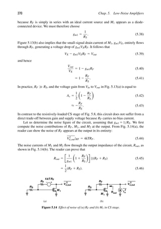
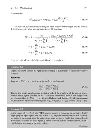
![272 Chap. 5. Low-Noise Amplifiers
Example 5.7 (Continued)
M 1
RF
VDD
M 2
out
V
I 1
C1
Vin
RS
Figure 5.15 CS stage with active load.
Solution:
For small-signal operation, M1 and M2 appear in parallel, behaving as a single transistor
with a transconductance of gm1 1 gm2. Thus, for input matching, gm1 1 gm2 5 1/RS. The
noise figure is still given by Eq. (5.49), except that γ (gm1 1 gm2)RS 5 γ . That is,
NF ≈ 1 1
4RS
RF
1 γ. (5.52)
This circuit is therefore superior, but it requires a supply voltage equal to VGS1 1 |VGS2| 1
VI1, where VI1 denotes the voltage headroom necessary for I1.
5.3.3 Common-Gate Stage
The low input impedance of the common-gate (CG) stage makes it attractive for LNA
design. Since a resistively-loaded stage suffers from the same gain-headroom trade-off as
its CS counterpart, we consider only a CG circuit with inductive loading [Fig. 5.16(a)].
Here, L1 resonates with the total capacitance at the output node (including the input capaci-
tance of the following stage), and R1 represents the loss of L1. If channel-length modulation
and body effect are neglected, Rin 5 1/gm. Thus, the dimensions and bias current of M1 are
chosen so as to yield gm 5 1/RS 5 (50 )21. The voltage gain from X to the output node
at the output resonance frequency is then equal to
Vout
VX
5 gmR1 (5.53)
5
R1
RS
(5.54)
and hence Vout/Vin 5 R1/(2RS).
Let us now determine the noise figure of the circuit under the condition gm 5 1/RS and
at the resonance frequency. Modeling the thermal noise of M1 as a voltage source in series](https://image.slidesharecdn.com/rfmicroelectronicsrazavi-230814101614-71259b59/85/RF-MICROELECTRONICS_Razavi-pdf-297-320.jpg)
![Sec. 5.3. LNA Topologies 273
Vb
M
Vin
RS
1
VDD
R
RS
(a) (b)
VDD
out
V
C
L1 R1
1
X
Rin
1
kT
4
g m
γ
M 1
V
2
n,out
Figure 5.16 (a) CG stage, (b) effect of noise of M1.
with its gate, V2
n1 5 4kTγ/gm [Fig. 5.16(b)], and multiplying it by the gain from the gate
of M1 to the output, we have
V2
n,out|M1 5
4kTγ
gm
⎛
⎜
⎜
⎝
R1
RS 1
1
gm
⎞
⎟
⎟
⎠
2
(5.55)
5 kTγ
R2
1
RS
. (5.56)
The output noise due to R1 is simply equal to 4kTR1. To obtain the noise figure, we divide
the output noise due to M1 and R1 by the gain and 4kTRS and add unity to the result:
NF 5 1 1
γ
gmRS
1
RS
R1
1 1
1
gmRS
2
(5.57)
5 1 1 γ 1 4
RS
R1
. (5.58)
Even if 4RS/R1 1 1 γ , the NF still reaches 3 dB (with γ ≈ 1), a price paid for the con-
dition gm 5 1/RS. In other words, a higher gm yields a lower NF but also a lower input
resistance. In Problem 5.8, we show that the NF can be lower if some impedance mismatch
is permitted at the input.
Example 5.8
We wish to provide the bias current of the CG stage by a current source or a resistor
(Fig. 5.17). Compare the additional noise in these two cases.
(Continues)](https://image.slidesharecdn.com/rfmicroelectronicsrazavi-230814101614-71259b59/85/RF-MICROELECTRONICS_Razavi-pdf-298-320.jpg)
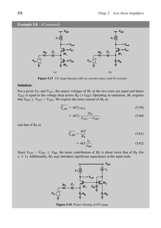
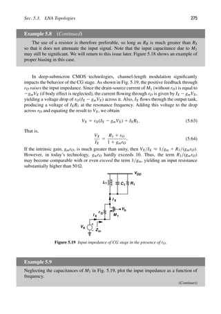
![276 Chap. 5. Low-Noise Amplifiers
Example 5.9 (Continued)
Solution:
At very low or very high frequencies, the tank assumes a low impedance, yielding
Rin 5 1/gm [or 1/(gm 1gmb) if body effect is considered]. Figure 5.20 depicts the behavior.
ω
ω0
( )
ω
Zin
1
g m
1
g m
+
R1
g m
rO
Figure 5.20 Input impedance of CG stage with a resonant load.
With the strong effect of R1 on Rin, we must equate the actual input resistance to RS to
guarantee input matching:
RS 5
R1 1 rO
1 1 gmrO
. (5.65)
The reader can prove that the voltage gain of the CG stage shown in Fig. 5.16(a) with a
finite rO is expressed as
Vout
Vin
5
gmrO 1 1
rO 1 gmrORS 1 RS 1 R1
R1, (5.66)
which, from Eq. (5.65), reduces to
Vout
Vin
5
gmrO 1 1
2
1 1
rO
R1
. (5.67)
This is a disturbing result! If rO and R1 are comparable, then the voltage gain is on the
order of gmrO/4, a very low value.
In summary, the input impedance of the CG stage is too low if channel-length mod-
ulation is neglected and too high if it is not! A number of circuit techniques have been
introduced to deal with the former case (Section 5.3.5), but in today’s technology, we face
the latter case.
In order to alleviate the above issue, the channel length of the transistor can be
increased, thus reducing channel-length modulation and raising the achievable gmrO. Since
the device width must also increase proportionally so as to retain the transconductance
value, the gate-source capacitance of the transistor rises considerably, degrading the input
return loss.](https://image.slidesharecdn.com/rfmicroelectronicsrazavi-230814101614-71259b59/85/RF-MICROELECTRONICS_Razavi-pdf-301-320.jpg)
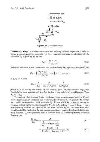
![278 Chap. 5. Low-Noise Amplifiers
R1
VDD
out
V
M 2
r CX
V
2
n2
2 O1
ω
r
2 O1 CX
1
r
2 O1 CX
g r
2 m2 O1 +1
g r
2 m2 O1 +1
(a) (b)
out
V
Vn2
g m2 R1
g m2 R1
Figure 5.22 (a) Cascode transistor noise, (b) output contribution as a function of frequency.
Figure 5.22(b) plots the frequency response, implying that the noise contribution of M2
is negligible for frequencies up to the zero frequency, (2rO1CX)21, but begins to mani-
fest itself thereafter. Since CX is comparable with CGS and 2rO1 1/gm, we note that
(2rO1CX)21 gm/CGS (≈ ωT). That is, the zero frequency is much lower than the fT of
the transistors, making this effect potentially significant.
Example 5.10
Assuming 2rO1 |CXs|21 at frequencies of interest so that the degeneration impedance in
the source of M2 reduces to CX, recompute the above transfer function while taking CGS2
into account. Neglect the effect of rO2.
Solution:
From the equivalent circuit shown in Fig. 5.23, we have gm2V1 5 2Vout/R1 and
hence V1 5 2Vout/(gm2R1). The current flowing through CGS2 is therefore equal to
2VoutCGS2s/(gm2R1). The sum of this current and 2Vout/R1 flows through CX, produc-
ing a voltage of [2VoutCGS2s/(gm2R1) 2 Vout/R1]/(CXs). Writing a KVL in the input loop
gives
2
VoutCGS2s
gm2R1
2
Vout
R1
1
CXs
2
Vout
gm2R1
5 Vin (5.73)
R1
VDD
out
V
M 2
Vin
C
CX
GS2
g
1 1
V V
CGS2
CX
Vin R1
out
V
m2
Figure 5.23 Computation of gain from the gate of cascode device to output.](https://image.slidesharecdn.com/rfmicroelectronicsrazavi-230814101614-71259b59/85/RF-MICROELECTRONICS_Razavi-pdf-303-320.jpg)
![Sec. 5.3. LNA Topologies 279
Example 5.10 (Continued)
and hence
Vout
Vin
5
2gm2R1CXs
(CGS2 1 CX)s 1 gm2
. (5.74)
At frequencies well below the fT of the transistor, |(CGS2 1 CX)s| gm2 and
Vout
Vin
≈ 2R1CXs. (5.75)
That is, the noise of M2 reaches the output unattenuated if ω is much greater than
(2rO1CX)21 [but much less than gm2/(CGS2 1 CX)].
The second issue stemming from the cascode device relates to the limited voltage head-
room. To quantify this limitation, let us determine the required or allowable values of Vb1
and Vb2 in Fig. 5.21. Since the drain voltage of M2 begins at VDD and can swing below
its gate voltage by as much as VTH2 while keeping M2 in saturation, we can simply choose
Vb2 5 VDD. Now, VX 5 VDD 2 VGS2, allowing a maximum value of VDD 2 VGS2 1 VTH1
for Vb1 if M1 must remain saturated. Consequently, the source voltage of M1 cannot exceed
VDD 2 VGS2 2 (VGS1 2 VTH1). We say the two transistors consume a voltage headroom of
one VGS plus one overdrive (VGS1 2 VTH1).
It may appear that, so long as VDD VGS2 1 (VGS1 2 VTH1), the circuit can be prop-
erly biased, but how about the path from the source of M1 to ground? In comparison with
the CG stages in Fig. 5.17, the cascode topology consumes an additional voltage head-
room of VGS1 2 VTH1, leaving less for the biasing transistor or resistor and hence raising
their noise contribution. For example, suppose ID1 5 ID2 5 2 mA. Since gm1 5 (50 )21 5
2ID/(VGS1 2 VTH1), we have VGS1 2 VTH1 5 200 mV. Also assume VGS2 ≈ 500 mV. Thus,
with VDD 5 1 V, the voltage available for a bias resistor, RB, tied between the source
of M1 and ground cannot exceed 300 mV/2 mA 5 150 . This value is comparable with
RS 5 50 and degrades the gain and noise behavior of the circuit considerably.
In order to avoid the noise-headroom trade-off imposed by RB, and also cancel the
input capacitance of the circuit, CG stages often employ an inductor for the bias path.
Illustrated in Fig. 5.24 with proper biasing for the input transistor, this technique minimizes
the additional noise due to the biasing element (LB) and significantly improves the input
matching. In modern RF design, both LB and L1 are integrated on the chip.
Design Procedure With so many devices present in the circuit of Fig. 5.24, how do we
begin the design? We describe a systematic procedure that provides a “first-order” design,
which can then be refined and optimized.
The design procedure begins with two knowns: the frequency of operation and the
supply voltage. In the first step, the dimensions and bias current of M1 must be chosen such
that a transconductance of (50 )21 is obtained. The length of the transistor is set to the
minimum allowable by the technology, but how should the width and the drain current be
determined?
Using circuit simulations, we plot the transconductance and fT of an NMOS transis-
tor with a given width, W0, as a function of the drain current. For long-channel devices,](https://image.slidesharecdn.com/rfmicroelectronicsrazavi-230814101614-71259b59/85/RF-MICROELECTRONICS_Razavi-pdf-304-320.jpg)
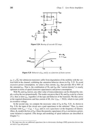
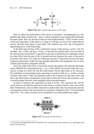
![282 Chap. 5. Low-Noise Amplifiers
In the last step, the value of the load inductor, L1, must be determined (Fig. 5.24). In a
manner similar to the choice of LB, we compute L1 such that it resonates with CGD2 1CDB2,
the input capacitance of the next stage, and its own capacitance. Since the voltage gain of
the LNA is proportional to R1 5 QL1ω, R1 must be sufficiently large, e.g., 500 to 1000 .
This condition is met in most designs without much difficulty.
The design procedure outlined above leads to a noise figure around 3 dB [Eq. (5.58)]
and a voltage gain, Vout/Vin 5 R1/(2RS), of typically 15 to 20 dB. If the gain is too high,
i.e., if it dictates an unreasonably high mixer IP3, then an explicit resistor can be placed in
parallel with R1 to obtain the required gain. As studied in Section 5.7, this LNA topology
displays a high IIP3, e.g., 15 to 110 dBm.
Example 5.11
Design the LNA of Fig. 5.24 for a center frequency of 5.5 GHz in 65-nm CMOS technology.
Assume the circuit is designed for an 11a receiver.
Solution:
Figure 5.28 plots the transconductance of an NMOS transistor with W 5 10 μm and L 5 60
nmasafunctionofthedraincurrent. Weselectabiascurrentof2 mAtoachieve a gm of about
10 mS 5 1/(100 ). Thus, to obtain an input resistance of 50 , we must double the width
and drain current.8 The capacitance introduced by a 20-μm transistor at the input is about
30 fF. To this we add a pad capacitance of 50 fF and choose LB 5 10 nH for resonance at
5.5 GHz. Such an inductor exhibits a parasitic capacitance of roughly 30 fF, requiring that
a smaller inductance be chosen, but we proceed without this refinement.
2.0
4.0
6.0
8.0
10.0
12.0
14.0
0.5 1.0 1.5 2.0 2.5 3.0
gm
(mS)
I D
(mA)
Figure 5.28 Transcoductance of a 10 μm/60 nm NMOS device as a function of drain current.
Next, we choose the width of the cascode device equal to 20 μm and assume a load
capacitance of 30 fF (e.g., the input capacitance of subsequent mixers). This allows the
use of a 10-nH inductor for the load, too, because the total capacitance at the output node
amounts to about 75 fF. However, with a Q of about 10 for such an inductor, the LNA
8. The body effect lowers the input resistance, but the feedback from the drain to the gate raises it. We therefore
neglect both.](https://image.slidesharecdn.com/rfmicroelectronicsrazavi-230814101614-71259b59/85/RF-MICROELECTRONICS_Razavi-pdf-307-320.jpg)
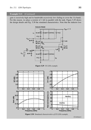
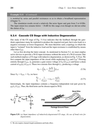
![Sec. 5.3. LNA Topologies 285
The third term in Eq. (5.77) carries a profound meaning: since gm/CGS1 ≈ ωT ( 5 2πfT),
the input resistance is approximately equal to L1ωT and directly related to the fT
of the transistor. For example, in 65-nm technology, ωT ≈ 2π 3 (160 GHz), dictating
L1 ≈ 50 pH (!) for a real part of 50 .
In practice, the degeneration inductor is often realized as a bond wire with the reason-
ing that the latter is inevitable in packaging and must be incorporated in the design. To
minimize the inductance, a “downbond” can directly connect the source pad to a ground
plane in the package [Fig. 5.31(b)], but even this geometry yields a value in the range of
0.5 to 1 nH—far from the 50-pH amount calculated above! That is, the input resistance
provided by modern MOSFETs tends to be substantially higher than 50 if a bond wire
inductance is used.10
How do we obtain a 50- resistance with L1 ≈ 0.5 nH? At operation frequencies far
below fT of the transistor, we can reduce the fT. This is accomplished by increasing the
channel length or simply placing an explicit capacitor in parallel with CGS. For example, if
L1 5 0.5 nH, then fT must be lowered to about 16 GHz.
Example 5.12
Determine the input impedance of the circuit shown in Fig. 5.32(a) if CGD is not neglected
and the drain is tied to a load resistance R1. Assume R1 ≈ 1/gm (as in a cascode).
M
V C
L1
P
X
I X
Zin
VDD
C
R1
1
GD
g
1 1
V V
C R1
L1
CGD
VX
I X
(a) (b)
GS m
GS
Figure 5.32 (a) Input impedance of CS stage in the presence of CGD, (b) equivalent circuit.
Solution:
From the equivalent circuit depicted in Fig. 5.32(b), we note the current flowing through
L1 is equal to V1CGSs 1 gmV1 and hence
VX 5 V1 1 (V1CGSs 1 gmV1)L1s. (5.78)
(Continues)
10. This is a rare case in which the transistor is too fast!](https://image.slidesharecdn.com/rfmicroelectronicsrazavi-230814101614-71259b59/85/RF-MICROELECTRONICS_Razavi-pdf-310-320.jpg)
![286 Chap. 5. Low-Noise Amplifiers
Example 5.12 (Continued)
Also, the current flowing through R1 is equal to IX 2 V1CGSs 2 gmV1, leading to
VX 5 (IX 2 V1CGSs 2 gmV1)R1 1 (IX 2 V1CGSs)
1
CGDs
. (5.79)
Substituting for V1 from (5.78), we have
VX
IX
5
R1 1
1
CGDs
(L1CGSs2
1 gmL1s 1 1)
L1CGSs2 1 (R1CGS 1 gmL1)s 1 gmR1 1 CGS/CGD 1 1
. (5.80)
If R1 ≈ 1/gm |CGDs|21 and CGS/CGD dominates in the denominator, (5.80) reduces to
VX
IX
≈
1
CGSs
1 L1s 1
gmL1
CGS
1 2
2CGD
CGS
2 L1CGDs2
2
R1CGD 1 gmL1
CGD
CGS
s
(5.81)
Assuming that the first two terms in the square brackets are dominant, we conclude that the
input resistance falls by a factor of 1 2 2CGD/CGS.
Effect of Pad Capacitance In addition to CGD, the input pad capacitance of the circuit
also lowers the input resistance. To formulate this effect, we construct the equivalent cir-
cuit shown in Fig. 5.33(a), where CGS1, L1, and R1 represent the three terms in Eq. (5.77),
respectively. Denoting the series combination jL1ω 2 j/(CGS1ω) by jX1 and 2j/(Cpadω)
by jX2, we first transform jX1 1 R1 to a parallel combination [Fig. 5.33(b)]. From
Chapter 2,
RP 5
X2
1
R1
. (5.82)
R
Cpad 1
L1 CGS1
Zin
R
Zin
P
1
jX
jX2 R
Zin
eq
1
X X 2
+
1
X X2
j
(a) (b) (c)
Figure 5.33 (a) Equivalent circuit for inclusion of pad capacitance, (b) simplified circuit of (a), (c)
simplified circuit of (b).](https://image.slidesharecdn.com/rfmicroelectronicsrazavi-230814101614-71259b59/85/RF-MICROELECTRONICS_Razavi-pdf-311-320.jpg)
![Sec. 5.3. LNA Topologies 287
We now merge the two parallel reactances into jX1X2/(X1 1X2) and transform the resulting
circuit to a series combination [Fig. 5.33(c)], where
Req 5
X1X2
X1 1 X2
2
·
1
RP
(5.83)
5
X2
X1 1 X2
2
R1. (5.84)
In most cases, we can assume L1ω 1/(CGS1ω) 1 1/(Cpadω) at the frequency of interest,
obtaining
Req ≈
CGS1
CGS1 1 Cpad
2
R1. (5.85)
For example, if CGS1 ≈ Cpad, then the input resistance falls by a factor of four.
We can now make two observations. First, the effect of the gate-drain and pad capac-
itance suggests that the transistor fT need not be reduced so much as to create R1 5 50 .
Second, since the degeneration inductance necessary for Re{Zin} 5 50 is insufficient to
resonate with CGS1 1Cpad, another inductor must be placed in series with the gate as shown
in Fig. 5.34, where it is assumed LG is off-chip.
M
C
L1
P
1
Vin
RS
Cpad
LG
GS
Figure 5.34 Addition of LG for input matching.
Example 5.13
A 5-GHz LNA requires a value of 2 nH for LG. Discuss what happens if LG is integrated
on the chip and its Q does not exceed 5.
Solution:
With Q 5 5, LG suffers from a series resistance equal to LGω/Q 5 12.6 . This value
is not much less than 50 , degrading the noise figure considerably. For this reason, LG is
typically placed off-chip.
NF Calculation Let us now compute the noise figure of the CS circuit, excluding the
effect of channel-length modulation, body effect, CGD, and Cpad for simplicity (Fig. 5.35).
The noise of M1 is represented by In1. For now, we assume the output of interest is the](https://image.slidesharecdn.com/rfmicroelectronicsrazavi-230814101614-71259b59/85/RF-MICROELECTRONICS_Razavi-pdf-312-320.jpg)
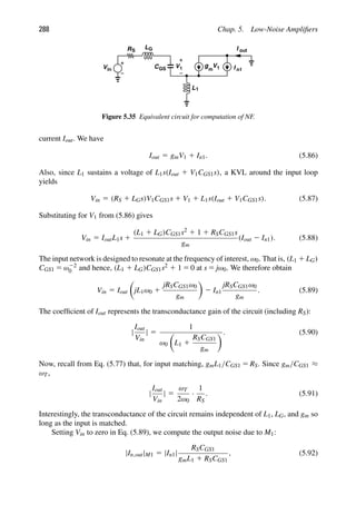
![Sec. 5.3. LNA Topologies 289
which, for gmL1/CGS1 5 RS, reduces to
|In,out|M1 5
|In1|
2
, (5.93)
and hence
I2
n,out|M1 5 kTγ gm. (5.94)
Dividing the output noise current by the transconductance of the circuit and by 4kTRS and
adding unity to the result, we arrive at the noise figure of the circuit [2]:
NF 5 1 1 gmRSγ
ω0
ωT
2
. (5.95)
It is important to bear in mind that this result holds only at the input resonance frequency
and if the input is matched.
Example 5.14
A student notes from Eq. (5.95) above that, if the transistor width and bias current are scaled
down proportionally, then gm and CGS1 decrease while gm/CGS1 5 ωT remains constant.
That is, the noise figure decreases while the power dissipation of the circuit also decreases!
Does this mean we can obtain NF 5 1 with zero power dissipation?
Solution:
As CGS1 decreases, LG 1 L1 must increase proportionally to maintain a constant ω0. Sup-
pose L1 is fixed and we simply increase LG. As CGS1 approaches zero and LG infinity, the Q
of the input network (≈ LGω0/RS) also goes to infinity, providing an infinite voltage gain at
the input. Thus, the noise of RS overwhelms that of M1, leading to NF 5 1. This result is not
surprising; after all, in a circuit such as the network of Fig. 5.36, |Vout/Vin| 5 (RSCaω0)21
at resonance, implying that the voltage gain approaches infinity if Ca goes to zero (and La
goes to infinity so that ω0 is constant). In practice, of course, the inductor suffers from a
finite Q (and parasitic capacitances), limiting the performance.
RS
Vin
L
Ca
out
V
a
Figure 5.36 Equivalent circuit of CS input network.
What if we keep LG constant and increase the degeneration inductance, L1? The NF still
approaches 1 but the transconductance of the circuit, Eq. (5.90), falls to zero if CGS1/gm
remains fixed.11 That is, the circuit provides a zero-dB noise figure but with zero gain.
11. If CGS1/gm is constant and L1 increases, the input cannot remain matched and Eq. (5.95) is invalid.](https://image.slidesharecdn.com/rfmicroelectronicsrazavi-230814101614-71259b59/85/RF-MICROELECTRONICS_Razavi-pdf-314-320.jpg)
![290 Chap. 5. Low-Noise Amplifiers
The above example suggests that maximizing LG can minimize the noise figure by
providing voltage gain from Vin to the gate of M1. The reader can prove that this gain is
given by
VG
Vin
5
1
2
1 1
LGω0
RS
. (5.96)
Note that LGω0/RS represents the Q of the series combination of LG and RS. Indeed, as
explained below, the design procedure begins with the maximum available value of LG
(typically an off-chip inductor) whose parasitic capacitances are negligible. The voltage
gain in the input network (typically as high as 6 dB) does lower the IP3 and P1dB of the
LNA, but the resulting values still prove adequate in most applications.
We now turn our attention to the output node of the circuit. As explained in
Section 5.3.1, an inductive load attached to a common-source stage introduces a negative
resistance due to the feedback through CGD. We therefore add a cascode transistor in the
output branch to suppress this effect. Figure 5.37 shows the resulting circuit, where R1 mod-
els the loss of LD. The voltage gain is equal to the product of the circuit’s transconductance
[Eq. (5.91)] and the load resistance, R1:12
Vout
Vin
5
ωT
2ω0
R1
RS
(5.97)
5
R1
2L1ω0
. (5.98)
The effect of CGD1 on the input impedance may still require attention because the
impedance seen at the source of M2, RX, rises sharply at the output resonance frequency.
From Eq. (5.64),
RX 5
R1 1 rO2
1 1 gmrO2
. (5.99)
M
L1
1
Vin
RS
LG
M 2
L C1 R1
VDD
out
V
D
RX
X
G
Figure 5.37 Inductively-degenerated cascode CS LNA.
12. The output impedance of the cascode is assumed much higher than R1.](https://image.slidesharecdn.com/rfmicroelectronicsrazavi-230814101614-71259b59/85/RF-MICROELECTRONICS_Razavi-pdf-315-320.jpg)
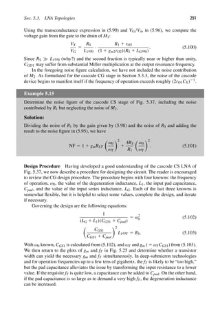
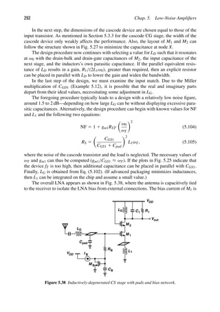
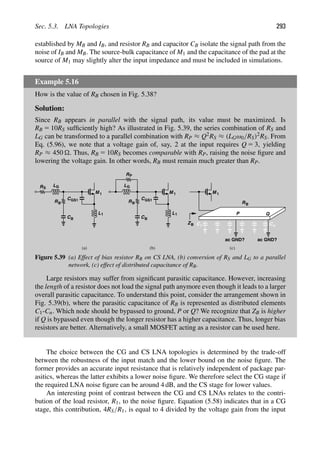
![294 Chap. 5. Low-Noise Amplifiers
source to the output. Thus, for a typical gain of 10, this contribution reaches 0.4, a sig-
nificant amount. For the inductively-degenerated CS stage, on the other hand, Eq. (5.101)
reveals that the contribution is equal to 4RS/R1 multiplied by (ω0/ωT)2. Thus, for opera-
tion frequencies well below the fT of the transistor, the noise contribution of R1 becomes
negligible.
Example 5.17
It is believed that input matching holds across a wider bandwidth for the CG stage than for
the inductively-degenerated CS stage. Is this statement correct?
Solution:
Consider the equivalent circuits shown in Fig. 5.40 for the two LNA configurations, where
R1 5 50 , C1 and C2 are roughly equal, and the inductors represent (inevitable) bond
L1
R1
C1
Zin1
L
R1
Z
g m
1
=
2
C2
CGS+ CSB
(a) (b)
in2
Figure 5.40 Input networks of (a) CS and (b) CG LNAs.
wires. For the CS stage [Fig. 5.40(a)], we have
Re{Zin1} 5 R1 (5.106)
Im{Zin1} 5
L1C1ω2 2 1
C1ω
. (5.107)
If the center frequency of interest is ω0 ( 5 1/
√
L1C1) and ω 5 ω0 1 ω, then
Im{Zin1} ≈ 2L1 ω
L1 ω
ω0
. (5.108)
That is, the imaginary part varies in proportion to deviation from the center frequency,
limiting the bandwidth across which |S11| remains acceptably low.
In the network of Fig. 5.40(b), on the other hand,
Re{Zin2} 5
R1
1 1 R2
1C2
2ω2
(5.109)
Im{Zin2} 5 L2ω 2
R2
1C2ω
1 1 R2
1C2
2ω2
. (5.110)](https://image.slidesharecdn.com/rfmicroelectronicsrazavi-230814101614-71259b59/85/RF-MICROELECTRONICS_Razavi-pdf-319-320.jpg)
![Sec. 5.3. LNA Topologies 295
Example 5.17 (Continued)
In practice, 1/(R1C2) is comparable with the ωT of the transistor [e.g., if R1 5 1/gm and
C2 5 CGS, then 1/(R1C2) ≈ ωT]. Thus, for ω ωT,
Re{Zin2} ≈ R1 (5.111)
Im{Zin2} ≈ (L2 2 R2
1C2)ω. (5.112)
Interestingly, if L2 5 R2
1C2, then Im{Zin2} falls to zero and becomes independent of fre-
quency. Thus the CG stage indeed provides a much broader band at its input, another
advantage of this topology.
Example 5.18
Design a cascode CS LNA for a center frequency of 5.5 GHz in 65-nm CMOS technology.
Solution:
We begin with a degeneration inductance of 1 nH and the same input transistor as that in the
CG stage of Example 5.11. Interestingly, with a pad capacitance of 50 fF, the input resis-
tance happens to be around 60 . (Without the pad capacitance, Re{Zin} is in the vicinity
of 600 .) We thus simply add enough inductance in series with the gate (LG 5 12 nH) to
null the reactive component at 5.5 GHz. The design of the cascode device and the output
network is identical to that of the CG example.
Figure 5.41 shows the details of the design and Fig. 5.42 the simulated characteristics.
We observe that the CS stage has a higher gain, a lower noise figure, and a narrower
bandwidth than the CG stage in Example 5.11.
VDD
10 nH 30 fF Ω
Ω
17
1 k
Ω
Inductor Model
6.9 k
= 1 V
20 μm
60 nm
20 μm
60 nm
1 pF
μm
60 nm
5
1 mA
Vout
30 fF
1 nH
Vin
RS
50 fF
12 nH Ω
10 k
Off Chip
Figure 5.41 CS LNA example.
(Continues)](https://image.slidesharecdn.com/rfmicroelectronicsrazavi-230814101614-71259b59/85/RF-MICROELECTRONICS_Razavi-pdf-320-320.jpg)
![296 Chap. 5. Low-Noise Amplifiers
Example 5.18 (Continued)
5 5.2 5.4 5.6 5.8 6
1.3
1.4
1.5
1.6
1.7
1.8
NF
(dB)
5 5.2 5.4 5.6 5.8 6
−20
−15
−10
−5
0
S11
(dB)
5 5.2 5.4 5.6 5.8 6
31
32
33
34
35
36
Frequency (GHz)
Gain
(dB)
5 5.2 5.4 5.6 5.8 6
−100
−50
0
50
100
Frequency (GHz)
Real
and
Imaginary
(Ω)
Re{Zin}
Im{Zin}
Figure 5.42 Simulated characteristics of CS LNA example.
5.3.5 Variants of Common-Gate LNA
As revealed by Eq. (5.57), the noise figure and input matching of the CG stage are inex-
tricably related if channel-length modulation is negligible, a common situation in older
CMOS technologies. For this reason, a number of efforts have been made to add another
degree of freedom to the design so as to avoid this relationship. In this section, we describe
two such examples.
Figure 5.43 shows a topology incorporating voltage-voltage feedback [3].13
The block
having a gain (or attenuation factor) of α senses the output voltage and subtracts a fraction
thereof from the input. (Note that M1 operates as a subtractor because ID1 ∝ VF 2 Vin.)
The loop transmission can be obtained by breaking the loop at the gate of M1 and is equal
to gmZL · α.14
If channel-length modulation and body effect are neglected, the closed-loop
input impedance is equal to the open-loop input impedance, 1/gm, multiplied by 11gmZLα:
Zin 5
1
gm
1 αZL. (5.113)
At resonance,
Zin 5
1
gm
1 αR1. (5.114)
13. This technique was originally devised for bipolar stages.
14. The input impedance of the feedback circuit is absorbed in ZL.](https://image.slidesharecdn.com/rfmicroelectronicsrazavi-230814101614-71259b59/85/RF-MICROELECTRONICS_Razavi-pdf-321-320.jpg)
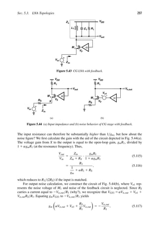
![298 Chap. 5. Low-Noise Amplifiers
and hence
Vn,out|M1 5
2gmVn1
gm(α 1
RS
R1
) 1
1
R1
. (5.118)
The noise current of R1 is multiplied by the output impedance of the circuit, Rout. The
reader can show that Rout is equal to R1 in parallel with (1 1 gmRS)/(αgm). Summing this
noise and that of M1, dividing the result by the square of (5.116) and 4kTRS, and assuming
the input is matched, we have
NF 5 1 1
γ
gmRS
1
RS
R1
1 1
1
gmRS
2
. (5.119)
That is, the NF can be lowered by raising gm. Note that this result is identical to that
expressed by Eq. (5.57) for the simple CG stage, except that gmRS need not be equal to
unity here. For example, if gmRS 5 4 and γ 5 1, then the first two terms yield a noise figure
of 0.97 dB. In Problem 5.15 we reexamine these results if channel-length modulation is not
neglected.
Example 5.19
How is the feedback factor, α, chosen in the above circuit?
Solution:
The design begins with the choice of gmRS and R1/(2RS) to obtain the required noise figure
and voltage gain, Av. For input matching, gmRS 2 1 5 αgmR1 5 αgm(2AvRS). It follows
that
α 5
gmRS 2 1
2gmRSAv
. (5.120)
For example, if gmRS 5 4 and Av 5 6 ( 5 15.6 dB), then R1 5 600 and α 5 1/16.
Another variant of the CG LNA employs feedforward to avoid the tight relationship
between the input resistance and the noise figure [4]. Illustrated in Fig. 5.45(a), the idea is
to amplify the input by a factor of 2A and apply the result to the gate of M1. For an input
voltage change of V, the gate-source voltage changes by 2(1 1 A) V and the drain
current by 2(1 1 A)gm V. Thus, the gm is “boosted” by a factor of 1 1 A [4], lowering
the input impedance to Rin 5 [gm(1 1 A)]21 and raising the voltage gain from the source
to the drain to (1 1 A)gmR1 (at resonance).
We now compute the noise figure with the aid of the equivalent circuit shown in Fig.
5.45(b). Since the current flowing through RS is equal to 2Vn,out/R1, the source voltage is
given by 2Vn,outRS/R1 and the gate voltage by (2Vn,outRS/R1)(2A) 1 Vn1. Multiplying](https://image.slidesharecdn.com/rfmicroelectronicsrazavi-230814101614-71259b59/85/RF-MICROELECTRONICS_Razavi-pdf-323-320.jpg)
![Sec. 5.3. LNA Topologies 299
L1 C1 R1
VDD
V
M 1
out
V
in
A
−
Rin
ΔV
R1
VDD
M 1
A
−
RS
Vn1
Vn,out
(a) (b)
Figure 5.45 (a) CG stage with feedforward, (b) calculation of NF.
the gate-source voltage by gm and equating the result to 2Vn,out/R1, we have
gm
A
RS
R1
Vn,out 1 Vn1 1
RS
R1
Vn,out
5 2
Vn,out
R1
, (5.121)
and hence
Vn,out|M1 5
2gmR1Vn1
(1 1 A)gmRS 1 1
. (5.122)
This expression reduces to 2gmR1Vn1/2 if the input is matched, indicating that half of the
noise current of M1 flows through R1.15
With input matching, the voltage gain from the left
terminal of RS in Fig. 5.45(b) to the output is equal to (1 1 A)gmR1/2. We therefore sum
the output noise contribution of M1 and R1, divide the result by the square of this gain and
the noise of RS, and add unity:
NF 5 1 1
γ
1 1 A
1
4RS
R1
. (5.123)
This equation reveals that the NF can be lowered by raising A with the constraint gm(1 1
A) 5 R21
S (for input matching).
The above analysis has neglected the noise of the gain stage A in Fig. 5.45(a). We show
in Problem 5.17 that the input-referred noise of this stage, V2
nA, is multiplied by A and added
to Vn1 in Eq. (5.122), leading to an overall noise figure equal to
NF 5 1 1
γ
1 1 A
1
4RS
R1
1
A2
(1 1 A)2
V2
nA
4kTRS
. (5.124)
In other words, V2
nA is referred to the input by a factor of A2/(1 1 A)2, which is not much
less than unity. For this reason, it is difficult to realize A by an active circuit.
It is possible to obtain the voltage gain through the use of an on-chip transformer. As
shown in Fig. 5.46 [4], for a coupling factor of k between the primary and the secondary and
15. Where does the other half go?](https://image.slidesharecdn.com/rfmicroelectronicsrazavi-230814101614-71259b59/85/RF-MICROELECTRONICS_Razavi-pdf-324-320.jpg)
![300 Chap. 5. Low-Noise Amplifiers
Vin
RS
VDD
out
V
C1
M
I 1
CB
M 1
2
L1
VDD
L2
k
Figure 5.46 CG stage with transformer feedforward.
a turns ratio of n ( 5
√
L2/L1), the transformer provides a voltage gain of kn. The direction
of the currents is chosen so as to yield a negative sign. However, on-chip transformer
geometries make it difficult to achieve a voltage gain higher than roughly 3, even with
stacked spirals [5]. Also, the loss in the primary and secondary contributes noise.
5.3.6 Noise-Cancelling LNAs
In our previous derivations of the noise figure of LNAs, we have observed three terms: a
value of unity arising from the noise of RS itself, a term representing the contribution of
the input transistor, and another related to the noise of the load resistor. “Noise-cancelling
LNAs” aim to cancel the second term [6]. The underlying principle is to identify two nodes
in the circuit at which the signal appears with opposite polarities but the noise of the input
transistor appears with the same polarity. As shown in Fig. 5.47, if nodes X and Y satisfy
this condition, then their voltages can be properly scaled and summed such that the signal
components add and the noise components cancel.
RS
Vin
X out
V
Y
A 0
LNA
Auxiliary Amplifier
Figure 5.47 Conceptual illustration of noise-cancelling LNAs.
The CS stage with resistive feedback studied in Section 5.3.2 serves as a good candidate
for noise cancellation because, as shown in Fig. 5.48(a), the noise current of M1 flows
through RF and RS, producing voltages at the gate and drain of the transistor with the
same polarity. The signal, on the other hand, experiences inversion. Thus, as conceptually
shown in Fig. 5.48(b), if VX is amplified by 2A1 and added to VY, the noise of M1 can
be removed [6]. Since the noise voltages at nodes Y and X bear a ratio of 1 1 RF/RS
(why?), we choose A1 5 11RF/RS. The signal experiences two additive gains: the original](https://image.slidesharecdn.com/rfmicroelectronicsrazavi-230814101614-71259b59/85/RF-MICROELECTRONICS_Razavi-pdf-325-320.jpg)
![Sec. 5.3. LNA Topologies 301
Y
M 1
RF
RS
Vin
out
V
X
Y
M 1
RF
RS
Vin
I n1
X
A
−
in
C
(a) (b)
1
Figure 5.48 (a) Noise of input transistor in a feedback CS stage, (b) cancellation of noise of M1.
gain, VY/VX 5 1 2 gmRF 5 1 2 RF/RS (if the input is matched), and the additional gain,
2(1 1 RF/RS). It follows that
Vout
VX
5 1 2
RF
RS
2
1 1
RF
RS
(5.125)
5 2
2RF
RS
, (5.126)
if the input is matched. The gain Vout/Vin is half of this value.
Let us now compute the noise figure of the circuit, assuming that the auxiliary amplifier
exhibits an input-referred noise voltage VnA1 and a high input impedance. Recall from
Section 5.3.2 that the noise voltage of RF appears directly at the output as 4kTRF. Adding
this noise to A2
1V2
nA1, dividing the result by (RF/RS)2 and 4kTRS, and adding unity, we
obtain the noise figure as
NF 5 1 1
RS
RF
1 A2
1V2
nA1
RS
4kTR2
F
. (5.127)
Since A1 5 1 1 RF/RS,
NF 5 1 1
RS
RF
1
V2
nA1
4kTRS
1 1
RS
RF
2
. (5.128)
The NF can therefore be minimized by maximizing RF and minimizing V2
nA1. Note that
RS/RF is the inverse of the gain and hence substantially less than unity, making the third
term approximately equal to V2
nA1/(4kTRS). That is, the noise of the auxiliary amplifier is
directly referred to the input and must therefore be much less than that of RS.
The input capacitance, Cin, arising from M1 and the auxiliary amplifier degrades both
S11 and the noise cancellation, thereby requiring a series (or parallel) inductor at the input
for operation at very high frequencies. It can be proved [6] that the frequency-dependent
noise figure is expressed as
NF( f) 5 NF(0) 1 [NF(0) 2 1 1 γ ]
f
f0
2
, (5.129)
where NF(0) is given by (5.128) and f0 5 1/(πRSCin).](https://image.slidesharecdn.com/rfmicroelectronicsrazavi-230814101614-71259b59/85/RF-MICROELECTRONICS_Razavi-pdf-326-320.jpg)
![302 Chap. 5. Low-Noise Amplifiers
X
Y
M 1
RF
RS
Vin
VDD
M
M
M
out
V
2
3
A
−
4
C1
RB
1
Figure 5.49 Example of noise-cancelling LNA.
Figure 5.49 depicts an implementation of the circuit [6]. Here, M2 and M3 serve as a CS
amplifier, providing a voltage gain of gm2/(gm3 1 gmb3), and also as the summing circuit.
Transistor M3 operates as a source follower, sensing the signal and noise at the drain of M1.
The first stage is similar to that studied in Example 5.7.
Example 5.20
Figure 5.50 shows an alternative implementation of a noise-cancelling LNA that also
performs single-ended to differential conversion. Neglecting channel-length modulation,
determine the condition for noise cancellation and derive the noise figure.
M 1
M
Vin
Vb1
R S
VDD
Vout
Vn1
2
R
R1 2
X
Y N
Figure 5.50 CG/CS stage as a noise-cancelling LNA.
Solution:
The circuit follows the noise cancellation principle because (a) the noise of M1, Vn1, sees a
source follower path to node X and a common-source path to node Y, exhibiting opposite
polarities at these two nodes, and (b) the signal sees a common-gate path through X and Y,
exhibiting the same polarity. Transistor M1 produces half of its noise voltage at X if the
input is matched (why?). Transistor M2 senses this noise and amplifies it by a factor of
2gm2R2. The reader can prove that the output noise of the CG stage due to M1 (at Y) is
equal to (Vn1/2)gm1R1. For noise cancellation, we must have
gm1R1
Vn1
2
5 gm2R2
Vn1
2
, (5.130)](https://image.slidesharecdn.com/rfmicroelectronicsrazavi-230814101614-71259b59/85/RF-MICROELECTRONICS_Razavi-pdf-327-320.jpg)
![Sec. 5.3. LNA Topologies 303
Example 5.20 (Continued)
and, since gm1 5 1/RS,
R1 5 gm2R2RS. (5.131)
If the noise of M1 is cancelled, the noise figure arises from the contributions of M2, R1,
and R2. The noise at Y is equal to 4kTR1 and at N equal to 4kTγ gm2R2
2 1 4kTR2. Since the
total voltage gain, Vout/Vin, is given by (gm1R1 1 gm2R2)/2 5 gm1R1 5 R1/RS, we have
NF 5 1 1
RS
R1
2
(4kTR1 1 4kTγ gm2R2
2 1 4kTR2)
1
4kTRS
(5.132)
5 1 1
RS
R1
1 γ
R2
R1
1
RSR2
R2
1
. (5.133)
The principal advantage of the above noise cancellation technique is that it affords the
broadband characteristics of feedback or CG stages but with a lower noise figure. It is there-
fore suited to systems operating in different frequency bands or across a wide frequency
range, e.g., 900 MHz to 5 GHz.
5.3.7 Reactance-Cancelling LNAs
It is possible to devise an LNA topology that inherently cancels the effect of its own
input capacitance. Illustrated in Fig. 5.51(a) [7], the idea is to exploit the inductive input
impedance of a negative-feedback amplifier so as to cancel the input capacitance, Cin. If
the open-loop transfer function of the core amplifier is modeled by a one-pole response,
A0/(1 1 s/ω0), then the input admittance is given by
Y1(s) 5
s 1 (A0 1 1)ω0
RF(s 1 ω0)
. (5.134)
Vin
R
R
Cin
Y 1
out
V
S
LNA
ω
ω0
F
RF
A0
1 +
1
Y1
Y1
Core
Amplifier
Re{ }
−Im{ }
(a) (b)
Figure 5.51 (a) Reactance-cancelling LNA topology, (b) behavior of components of Y1 with
frequency.](https://image.slidesharecdn.com/rfmicroelectronicsrazavi-230814101614-71259b59/85/RF-MICROELECTRONICS_Razavi-pdf-328-320.jpg)
![304 Chap. 5. Low-Noise Amplifiers
It follows that
1
Re{Y1}
5
RF(ω2 1 ω2
0)
(1 1 A0)ω2
0
(5.135)
Im{Y1} 5
2A0ωω0
RF(ω2 1 ω2
0)
. (5.136)
At frequencies well below ω0, 1/Re{Y1} reduces to RF/(1 1 A0), which can be set
equal to RS, and Im{Y1} is roughly 2A0ω/(RFω0), which can be chosen to cancel Cinω.
Figure 5.51(b) illustrates the behavior of 1/Re{Y1} and 2Im{Y1}.
The input matching afforded by the above technique holds for frequencies up to about
ω0, dictating that the open-loop bandwidth of the core amplifier reach the maximum fre-
quency of interest. The intrinsic speed of deep-submicron devices provides the gain and
bandwidth required here.
The reader may wonder if our modeling of the core amplifier by a one-pole response
applies to multistage implementations as well. We return to this point below.
Figure 5.52 shows a circuit realization of the amplifier concept for the frequency range
of 50 MHz to 10 GHz [7]. Three common-source stages provide gain and allow negative
feedback. Cascodes and source followers are avoided to save voltage headroom. The input
transistor, M1, has a large width commensurate with flicker noise requirements at 50 MHz,
thus operating with a VGS of about 200 mV. If this voltage also appears at node Y, it leaves
no headroom for output swings, limiting the linearity of the circuit. To resolve this issue,
current I1 is drawn from RF so as to shift up the quiescent voltage at Y by approximately
250 mV. Since RF 5 1 k, I1 need be only 200 μA, contributing negligible noise at the
LNA input.16
With three gain stages, the LNA can potentially suffer from a small phase margin
and exhibit substantial peaking in its frequency response. In this design, the open-loop
poles at nodes A, B, X, and Y lie at 10 GHz, 24.5 GHz, 22 GHz, and 75 GHz, respec-
tively, creating a great deal of phase shift. Nonetheless, due to the small feedback factor,
Vin
RS
M 1 M 2
200 m
μ
60 nm
75 Ω Ω Ω
m
μ
60 nm
25
200 150
M
m
μ
60 nm
25
3
VDD
Ω
1000
A
B X
Y
RF
I 1
Figure 5.52 Implementation of reactance-cancelling LNA.
16. Alternatively, capacitive coupling can be used in the feedback path. But the large value necessary for the
capacitor would introduce additional parasitics.](https://image.slidesharecdn.com/rfmicroelectronicsrazavi-230814101614-71259b59/85/RF-MICROELECTRONICS_Razavi-pdf-329-320.jpg)
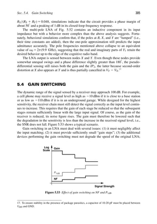
![306 Chap. 5. Low-Noise Amplifiers
M
L1
in
V
M
M
VDD
M
I 1
1x
1y
GS
GS
L1
Vout
2
3
Figure 5.54 Example of gain switching in CG stage.
(4) for high input signal levels, gain switching must also make the LNA more linear so that
this stage does not limit the receiver linearity. As seen below, some LNA topologies lend
themselves more easily to gain switching than others do.
Let us first consider a common-gate stage. Can we reduce the transconductance of the
input transistor to reduce the gain? To switch the gain while maintaining input matching,
we can insert a physical resistance in parallel with the input as gm is lowered. Figure 5.54
shows an example [8], where the input transistor is decomposed into two, M1x and M1y,
and transistor M2 introduces a parallel resistance if it is on. In the “high-gain mode,” the
gain select line, GS, is high, placing M1x and M1y in parallel, and M2 is off. In the “low-
gain mode,” M1y turns off, reducing the gain, and M2 turns on, ensuring that Ron2||(gm1x 1
gmb1x)21 5 RS. For example, to reduce the gain by 6 dB, we choose equal dimensions for
M1x and M1y and Ron2 5 (gm1x 1 gmb1x)21 5 2RS (why?). Also, the gate of M1y is secured
to ground by a capacitor to avoid the on-resistance of the switch at high frequencies.
Example 5.21
Choose the devices in the above circuit for a gain step of 3 dB.
Solution:
To reduce the voltage gain by
√
2, we have
W1x
W1x 1 W1y
5
1
√
2
, (5.137)
and hence W1y/W1x 5
√
2 2 1. We also note that, with M1y off, the input resistance rises to
√
2RS. Thus, Ron2||(
√
2RS) 5 RS and hence
Ron2 5
√
2
√
2 2 1
RS. (5.138)
In Problem 5.21, we calculate the noise figure after the 3-dB gain reduction.](https://image.slidesharecdn.com/rfmicroelectronicsrazavi-230814101614-71259b59/85/RF-MICROELECTRONICS_Razavi-pdf-331-320.jpg)
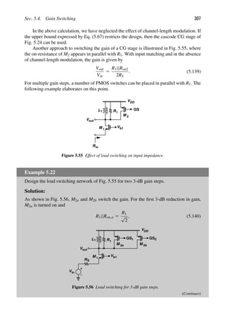
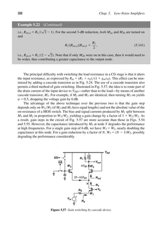
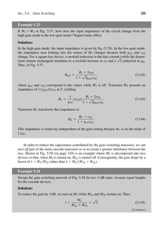
![310 Chap. 5. Low-Noise Amplifiers
Example 5.24 (Continued)
For another 3-dB reduction, we turn off M2b:
1 1
W3
W2a
5 2. (5.146)
It follows from Eqs. (5.145) and (5.146) that
W3 5 W2a 5
W2b
√
2
. (5.147)
In a more aggressive design, M2 would be decomposed into three devices, such that
one is turned off for the first 3-dB step, allowing M3 to be narrower. The calculations are
left as an exercise for the reader.
VDD
Vin
RS
V
M 1
M
b
M 3
GS
GS
M
2a 2b
Figure 5.58 Gain switching by programmable cascode devices.
We now turn our attention to gain switching in an inductively-degenerated cascode
LNA. Can we switch part of the input transistor to switch the gain (Fig. 5.59)? Turning M1b
off does not alter ωT because the current density remains constant. Thus, Re{Zin} 5 L1ωT
is relatively constant, but Im{Zin} changes, degrading the input match. If the input match
is somehow restored, then the voltage gain, R1/(2L1ω), does not change! Furthermore, the
thermal noise of S1 degrades the noise figure in the high gain mode. For these reasons, gain
switching must be realized in other parts of the circuit.
As with the CG LNA of Fig. 5.55, the gain can be reduced by placing one or more
PMOS switches in parallel with the load [Fig. 5.60(a)]. Alternatively, the cascode switching
scheme of Fig. 5.57 can be applied here as well [Fig. 5.60(b)]. The latter follows the
calculations outlined in Example 5.24, providing well-defined gain steps with a moderate](https://image.slidesharecdn.com/rfmicroelectronicsrazavi-230814101614-71259b59/85/RF-MICROELECTRONICS_Razavi-pdf-335-320.jpg)
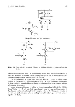
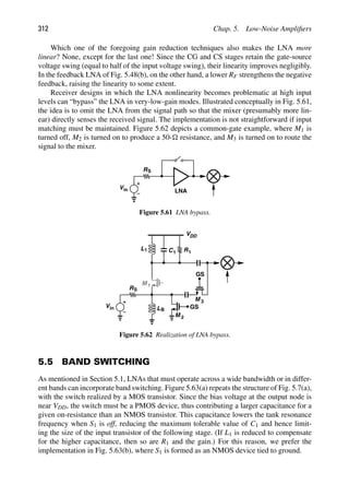
![Sec. 5.6. High-IP2 LNAs 313
(a)
L1 C1 R1
VDD
C2 M a
out
V
CGD1
CDB1
Band
Switch
1
S
L1 C1 R1
VDD
C2 M a
out
V
Band
Switch
1
S
(b)
Figure 5.63 (a) Band switching, (b) effect of switch parasitics.
The choice of the width of S1 in Fig. 5.63(b) proves critical. For a very narrow transis-
tor, the on-resistance, Ron1, remains so high that the tank does not “feel” the presence of
C2 when S1 is on. For a moderate device width, Ron1 limits the Q of C2, thereby lowering
the Q of the overall tank and hence the voltage gain of the LNA. This can be readily seen
by transforming the series combination of C2 and Ron1 to a parallel network consisting of
C2 and RP1 ≈ Q2Ron1, where Q 5 (C2ωRon1)21. That is, R1 is now shunted by a resistance
RP1 5 (C2
2ω2Ron1)21.
The foregoing observation implies that Ron1 must be minimized such that RP1 R1.
However, as the width of S1 in Fig. 5.63(b) increases, so does the capacitance that it intro-
duces in the off state. The equivalent capacitance seen by the tank when S1 is off is equal
to the series combination of C2 and CGD1 1 CDB1, which means C1 must be less than its
original value by this amount. We therefore conclude that the width of S1 poses a trade-off
between the tolerable value of C1 when S1 is off and the reduction of the gain when S1 is
on. (Recall that C1 arises from Ma, the input capacitance of the next stage, and the parasitic
capacitance of L1.)
An alternative method of band switching incorporates two or more tanks as shown in
Fig. 5.64 [8]. To select one band, the corresponding cascode transistor is turned on while
the other remains off. This scheme requires that each tank drive a copy of the following
stage, e.g., a mixer. Thus, when M1 and band 1 are activated, so is mixer MX1. The prin-
cipal drawback of this approach is the capacitance contributed by the additional cascode
device(s) to node Y. Also, the spiral inductors have large footprints, making the layout and
routing more difficult.
5.6 HIGH-IP2 LNAS
As explained in Chapter 4, even-order distortion can significantly degrade the performance
of direct-conversion receivers. Since the circuits following the downconversion mixers are
typically realized in differential form,18
they exhibit a high IP2, leaving the LNA and the
18. And since they employ large devices and hence have small mismatches.](https://image.slidesharecdn.com/rfmicroelectronicsrazavi-230814101614-71259b59/85/RF-MICROELECTRONICS_Razavi-pdf-338-320.jpg)
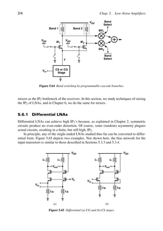
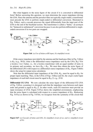
![316 Chap. 5. Low-Noise Amplifiers
we can compute the output noise of each half circuit as in Fig. 5.67(c) and add the output
powers:
V2
n,out 5 V2
n,out1 1 V2
n,out2. (5.148)
Since each half circuit provides matching at the input, the CG results of Section 5.3.3
apply here as well with the substitution RS 5 RS1/2. Specifically, the voltage gain from
X to Y is equal to R1/(2RS1/2), where R1 denotes the load resistance of the CG half cir-
cuit. The output noise consists of (1) the input transistor contribution, given by Eq. (5.56),
(2) the load resistor contribution, 4kTR1, and (3) the source impedance contribution,
(4kTRS1/2)[R1/(2R1/2)]:
V2
n,out1 5 kTγ
R2
1
RS1/2
1 4kTR1 1 4kT
RS1
2
⎛
⎜
⎝
R1
2RS1
2
⎞
⎟
⎠
2
. (5.149)
From Eq. (5.148), the total output noise power is twice this amount. Noting that the total
voltage gain Av 5 (VY 2 VW)/(VX 2 VZ) is equal to that of half of the circuit, VY/VX
( 5 R1/RS1), we compute the noise figure with respect to a source impedance of RS1 as
NF 5
V2
n,out
A2
v
·
1
4kTRS1
(5.150)
5 1 1 γ 1
2RS1
R1
. (5.151)
Interestingly, this value is lower than that of the single-ended counterpart [Eq. (5.58)]. But
why? Since in Fig. 5.67(c), VY/VX 5 R1/(2RS1/2) 5 R1/RS1, we observe that the voltage
gain is twice that of the single-ended CG LNA. (After all, the transconductance of the
input transistor is doubled to lower the input impedance to RS1/2.) On the other hand, the
overall differential circuit contains two R1’s at its output, each contributing a noise power
of 4kTR1. The total, 8kTR1, divided by (R1/RS1)2 and 4kTRS1 yields 2RS1/R1. Of course,
the value stipulated by Eq. (5.151) can be readily obtained in a single-ended CG LNA
by simply doubling the load resistance. Figure 5.68 summarizes the behavior of the two
circuits, highlighting the greater voltage gain in the differential topology. If identical gains
are desired, the value of the load resistors in the differential circuit must be halved, thereby
yielding identical noise figures.
In summary, a single-ended CG LNA can be converted to differential form according
to one of three scenarios: (1) simply copy the circuit, in which case the differential input
resistance reaches 100 , failing to provide matching with a 1-to-1 balun; (2) copy the
circuit but double the transconductance of the input transistors, in which case the input is
matched but the overall voltage gain is doubled; (3) follow the second scenario but halve the
load resistance to retain the same voltage gain. The second choice is generally preferable.
Note that, for a given noise figure, a differential CG LNA consumes four times the power
of a single-ended stage.19
19. To halve the input resistance, the transistor width and bias current must be doubled.](https://image.slidesharecdn.com/rfmicroelectronicsrazavi-230814101614-71259b59/85/RF-MICROELECTRONICS_Razavi-pdf-341-320.jpg)
![Sec. 5.6. High-IP2 LNAs 317
R
Vin
R1
V
V R1
R
2
RS1
CG LNA
R
R
Vin
RS1
S1
1:1
S1 R1 R1
V
V R1
R
2
(a)
(b)
S1
S1
S1
p
p
V R1
R
2 S1
p
p
p
Figure 5.68 Comparison of (a) single-ended and (b) differential CG LNAs.
Our NF calculations have assumed an ideal balun. In reality, even external baluns have
a loss as high as 0.5 dB, raising the NF by the same amount.
Example 5.25
An amplifier having a high input impedance employs a parallel resistor at the input to
provide matching [Fig. 5.69(a)]. Determine the noise figure of the circuit and its differential
version, shown in Fig. 5.69(b), where two replicas of the amplifier are used.
R
Vin
S1
RS1
V
2
n
A
R
Vin
1:1
S1
RS1
2
V
2
n
A
RS1
2
A
V
2
n
A
RS1
2
RS1
2
V
2
n,out1
(a) (b) (c)
Figure 5.69 (a) NF of an LNA with resistive termination, (b) differential version of (a), (c) simplified
circuit of (b).
Solution:
In the circuit of Fig. 5.69(a), the amplifier input-referred noise current is negligible and
the total noise at the output is equal to (4kTRS1/2)A2 1 A2V2
n . The noise figure of the
(Continues)](https://image.slidesharecdn.com/rfmicroelectronicsrazavi-230814101614-71259b59/85/RF-MICROELECTRONICS_Razavi-pdf-342-320.jpg)
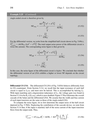
![Sec. 5.6. High-IP2 LNAs 319
R
Vin
1:1
S1
RS1
2
V
2
n,out1
(a)
VDD
L
Vout
L
(b)
in
R 1
2
L1
2
LG
LD D
RS1
R1
R1 LD
R1
VDD
RS1
2
L1
2
L
2
G
M 1
Figure 5.70 (a) Differential CS LNA and (b) its half circuit.
Multiplying this power by two, dividing it by A2
v 5 R2
1/(L1ω0)2 and 4kTRS1, and noting
that L1ωT/2 5 RS1/2, we have
NF 5
γ
2
gm1RS1
ω0
ωT
2
1
2RS1
R1
ω0
ωT
2
1 1. (5.157)
How does this compare with the noise figure of the original single-ended LNA
[Eq. (5.101)]? We observe that both the transistor contribution and the load contribution
are halved. The transistor contribution is halved because gm1 and hence the transistor noise
current remain unchanged while the overall transconductance of the circuit is doubled.
To understand this point, recall from Section 5.3.4 that Gm 5 ωT/(2ω0RS) for the original
single-ended circuit. Now consider the equivalent circuit shown in Fig. 5.71, where the dif-
ferential transconductance, (I1 2 I2)/Vin, is equal to ωT/(ω0RS1) (why?). The differential
output current contains the noise currents of both M1 and M2 and is equal to 2(kTγ gm1).
If this power is divided by the square of the transconductance and 4kTRS1, the first term in
Eq. (5.157) is obtained.
RS1
2
L1
2
L
2
G
I 1
RS1
2
L1
2
L
2
G
I 2
Vin
Figure 5.71 Differential CS stage viewed as a transconductor.](https://image.slidesharecdn.com/rfmicroelectronicsrazavi-230814101614-71259b59/85/RF-MICROELECTRONICS_Razavi-pdf-344-320.jpg)
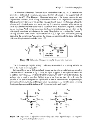
![Sec. 5.6. High-IP2 LNAs 321
The capacitance at P can be nulled through the use of a parallel inductor [Fig. 5.73(b)]
[9], but the CGD1 feedforward persists. The tail inductor can be realized on-chip because
its parallel equivalent resistance at resonance (RP 5 QLPω0) is typically much greater than
1/gm1,2.
Example 5.26
A student computes CP in Fig. 5.73(b) as CSB1 1 CSB2 1 CGS2, and selects the value of LP
accordingly. Is this an appropriate choice?
Solution:
No, it is not. For LP to null the phase shift at P, it must resonate with only CSB1 1 CSB2.
This point can be seen by examining the voltage division at node P. As shown in Fig. 5.74,
in the absence of CSB1 1 CSB2,
VP 5 Vin
Z2
Z1 1 Z2
. (5.158)
M M
1 2
in
V
P
CGS1 CGS2
Z 2
Z 1
Figure 5.74 Impedances seen at the common source of differential pair.
For VP to be exactly equal to half of Vin (with zero phase difference), we must have Z1 5 Z2.
Since each impedance is equal to (gm 1 gmb)21||(CGSs)21, we conclude that CGS2 must
not be nulled.20
The topology of Fig. 5.73(b) still does not provide input matching. We must therefore
insert (on-chip) inductances in series with the sources of M1 and M2 (Fig. 5.75). Here, LP1
and LP2 resonate with CP1 and CP2, respectively, and LS1 1 LS2 provides the necessary
input resistance. Of course, LS1 1 LS2 is realized as one inductor. However, as explained in
Section 5.7, this topology exhibits a lower IP3 than that of Fig. 5.65(b).
Balun Issues The foregoing development of differential LNAs has assumed ideal 1-to-1
baluns. Indeed, external baluns with a low loss (e.g., 0.5 dB) in the gigahertz range are
available from manufacturers, but they consume board space and raise the cost. Inte-
grated baluns, on the other hand, suffer from a relatively high loss and large capacitances.
20. But the parasitic capacitance of ISS must be nulled.](https://image.slidesharecdn.com/rfmicroelectronicsrazavi-230814101614-71259b59/85/RF-MICROELECTRONICS_Razavi-pdf-346-320.jpg)
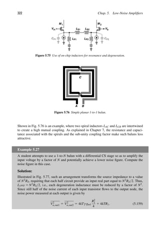
![Sec. 5.6. High-IP2 LNAs 323
Example 5.27 (Continued)
R
Vin
VDD
L
L
R 1 L1
LG
LD D
RS
S
N
2
S
R
N
2
S
1:N
V
2
n,out1 V
2
n,out2
Vb
R
R 1
1
Figure 5.77 Use of 1-to-N balun in an LNA.
The gain from Vin to the differential output is now equal to NR1/(2L1ω0). Doubling the
above power, dividing by the square of the gain, and normalizing to 4kTRS, we have
NF 5 N2 γ
2
gm1RS
ω0
ωT
2
1 2N2 RS
R1
ω0
ωT
2
1 1. (5.160)
We note, with great distress, that the first two terms have risen by a factor of N2!21 This
is because the condition L1ωT 5 N2RS/2 inevitably leads to an N2-fold reduction in the
transconductance of the circuit. Thus, even with the N-fold amplification of Vin by the
balun, the overall voltage gain drops by a factor of N.
The reader may wonder if an N-to-1 (rather than 1-to-N) balun proves beneficial in
the above example as it would multiply the first two terms of Eq. (5.160) by 1/N2 rather
than N2. Indeed, off-chip baluns may provide a lower noise figure if L1 (a bond wire) can be
reduced by a factor of N2. On the other hand, on-chip baluns with a non-unity turns ratio are
difficult to design and suffer from a higher loss and a lower coupling factor. Figure 5.78(a)
shows an example [5], where one spiral forms the primary (secondary) of the balun and
the series combination of two spirals constitutes the secondary (primary). Alternatively, as
shown in Fig. 5.78(b), spirals having different numbers of turns can be embedded [10].
5.6.2 Other Methods of IP2 Improvement
The difficulty with the use of off-chip or on-chip baluns at the input of differential LNAs
makes single-ended topologies still an attractive choice. A possible approach to raising the
IP2 entails simply filtering the low-frequency second-order intermodulation product, called
the beat component in Chapter 4. Illustrated in Fig. 5.79, the idea is to remove the beat by
a simple high-pass filter (HPF) following the LNA. For example, suppose two interferers
21. Assuming that gm1 and ωT remain unchanged.](https://image.slidesharecdn.com/rfmicroelectronicsrazavi-230814101614-71259b59/85/RF-MICROELECTRONICS_Razavi-pdf-348-320.jpg)
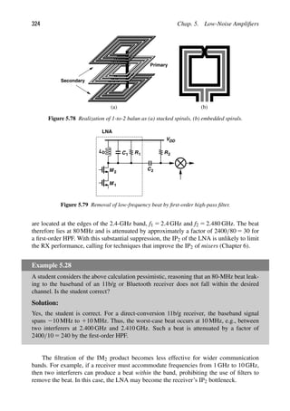
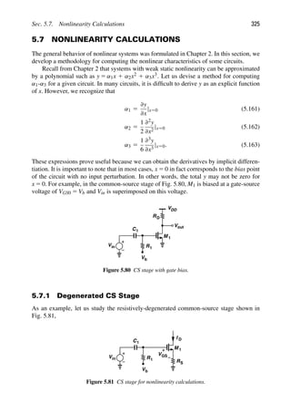
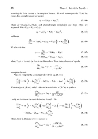
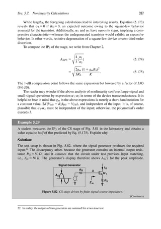
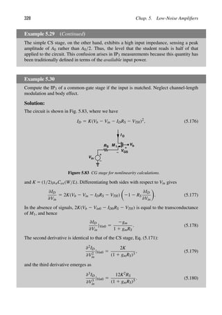
![Sec. 5.7. Nonlinearity Calculations 329
Example 5.30 (Continued)
Thus, the IP3 expression in Eq. (5.175) applies here as well. For input matching, RS 5 1/gm.
However, as explained in Example 5.29, the definition of IP3 is based on the available
signal power, i.e., that which is delivered to a matched load. Thus, the peak value predicted
by Eq. (5.175) must be divided by 2, yielding
AIIP3 5
2
K
2
3
gm (5.181)
5 4
2
3
(VGS0 2 VTH), (5.182)
where VGS0 denotes the bias value of the gate-source voltage.
5.7.2 Undegenerated CS Stage
Consider the CS stage shown in Fig. 5.80. Submicron transistors substantially depart from
square-law characteristics. The effect of mobility degradation due to both vertical and
lateral fields in the channel can be approximated as
ID 5
1
2
μ0Cox
W
L
(VGS 2 VTH)2
1 1 (
μ0
2vsatL
1 θ)(VGS 2 VTH)
, (5.183)
where μ0 denotes the zero-field mobility, vsat the saturation velocity of the carriers, and θ
the effect of the vertical field [11]. If the second term in the denominator remains much less
than unity, we can write (1 1 ε)21 ≈ 1 2 ε and hence
ID ≈
1
2
μ0Cox
W
L
(VGS 2 VTH)2
2
μ0
2vsatL
1 θ
(VGS 2 VTH)3
. (5.184)
The input signal, Vin, is superimposed on a bias voltage, VGS0 5 Vb. We therefore replace
VGS with Vin 1 VGS0, obtaining
ID ≈ K[2 2 3a(VGS0 2 VTH)](VGS0 2 VTH)Vin 1 K[1 2 3a(VGS0 2 VTH)]V2
in
2 KaV3
in 1 K(VGS0 2 VTH)2
2 aK(VGS0 2 VTH)3
, (5.185)
where K 5 (1/2)μ0Cox(W/L) and a 5 μ0/(2vsatL)1θ. We recognize the coefficient of Vin
as the transconductance (∂ID/∂Vin) and the last two terms as the bias current. It follows
that
α1 5 K[2 2 3a(VGS0 2 VTH)](VGS0 2 VTH) (5.186)
α3 5 2Ka. (5.187)](https://image.slidesharecdn.com/rfmicroelectronicsrazavi-230814101614-71259b59/85/RF-MICROELECTRONICS_Razavi-pdf-354-320.jpg)
 (5.191)
α3 5 2Ka[1 2 4a(VGS0 2 VTH)]. (5.192)](https://image.slidesharecdn.com/rfmicroelectronicsrazavi-230814101614-71259b59/85/RF-MICROELECTRONICS_Razavi-pdf-355-320.jpg)
![Problems 333
this fact, we have
∂3ID1
∂V3
in
|Vin50 5
23
(RS 1
2
gm
)4
gmI2
0
5 6α3. (5.203)
It follows that 6α3 5 ∂3(ID1 2 ID2)/∂V3
in 5 2∂3ID1/∂V3
in. We now have that
AIIP3 5
2I0
3
gm
RS 1
2
gm
3
. (5.204)
REFERENCES
[1] J. Rogin et al., “A 1.5-V 45-mW Direct-Conversion WCDMA Receiver IC in 0.13-m CMOS,”
IEEE Journal of Solid-State Circuits, vol. 38, pp. 2239–2248, Dec. 2003.
[2] D. K. Shaeffer and T. H. Lee, “A 1.5-V, 1.5-GHz CMOS Low Noise Amplifier,” IEEE J.
Solid-State Circuits, vol. 32, pp. 745–759, May 1997.
[3] P. Rossi et al., “A Variable-Gain RF Front End Based on a Voltage-Voltage Feedback LNA for
Multistandard Applications,” IEEE J. Solid-State Circuits, vol. 40, pp. 690–697, March 2005.
[4] X. Li, S. Shekar, and D. J. Allstot, “Gm-Boosted Common-Gate LNA and Differential Col-
pitts VCO/QVCO in 0.18-um CMOS,” IEEE J. Solid-State Circuits, vol. 40, pp. 2609–2618,
Dec. 2005.
[5] A. Zolfaghari, A. Y. Chan, and B. Razavi, “Stacked Inductors and 1-to-2 Transformers in
CMOS Technology,” IEEE Journal of Solid-State Circuits, vol. 36, pp. 620–628, April 2001.
[6] F. Bruccoleri, E. A. M. Klumperink, and B. Nauta, “Wideband CMOS Low-Noise Amplifier
Exploiting Thermal Noise Canceling,” IEEE J. Solid-State Circuits, vol. 39, pp. 275–281,
Feb. 2004.
[7] B. Razavi, “Cognitive Radio Design Challenges and Techniques,” IEEE Journal of Solid-State
Circuits, vol. 45, pp. 1542–1553, Aug. 2010.
[8] B. Razavi et al., “A UWB CMOS Transceiver,” IEEE Journal of Solid-State Circuits, vol. 40,
pp. 2555–2562, Dec. 2005.
[9] M. Zargari et al., “A Single-Chip Dual-Band Tri-Mode CMOS Transceiver for IEEE
802.11a/b/g Wireless LAN,” IEEE Journal of Solid-State Circuits, vol. 39, pp. 2239–2249,
Dec. 2004.
[10] J. R. Long and M. A. Copeland, “The Modeling, Characterization, and Design of Monolithic
Inductors for Silicon RF ICs,” IEEE J. Solid-State Circuits, vol. 32, pp. 357–369, March 1997.
[11] B. Razavi, Design of Analog CMOS Integrated Circuits, Boston: McGraw-Hill, 2001.
PROBLEMS
5.1. Assuming Zin 5 x 1 jy, derive an equation for constant- contours in Fig. 5.4.
5.2. If Rp 5 RS and gmRS ≈ 1, determine the NF in Eq. (5.18) by considering the first
three terms. What value of gm is necessary to achieve a noise figure of 3.5 dB?
5.3. Repeat Example 5.5 by solving the specific network shown in Fig. 5.10(a).
5.4. Determine the noise figure of the stages shown in Fig. 5.87 with respect to a source
impedance of RS. Neglect channel-length modulation and body effect.](https://image.slidesharecdn.com/rfmicroelectronicsrazavi-230814101614-71259b59/85/RF-MICROELECTRONICS_Razavi-pdf-358-320.jpg)
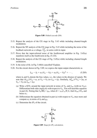
![336 Chap. 5. Low-Noise Amplifiers
5.21. Determine the noise figure in Example 5.21 if the gain is reduced by 3 dB.
5.22. Compare the power consumptions of the single-ended and differential CS stages
discussed in Section 5.6.1. Consider two cases: (a) the differential stage is derived
by only halving L1 (and hence has a lower noise figure), or (b) the differential stage
is designed for the same NF as the single-ended circuit.
5.23. Repeat the analysis of the differential CG stage NF if a 1-to-2 balun is used. Such a
balun provides a voltage gain of 2.
5.24. Consider a MOS transistor configured as a CS stage and operating in saturation.
Determine the IP3 and P1dB if the device (a) follows the square-law behavior, ID ∝
(VGS 2 VTH)2, or (b) exhibits field-dependent mobility [Eq. (5.183)]. (Hint: IP3 and
P1dB may not be related by a 9.6-dB difference in this case.)](https://image.slidesharecdn.com/rfmicroelectronicsrazavi-230814101614-71259b59/85/RF-MICROELECTRONICS_Razavi-pdf-361-320.jpg)

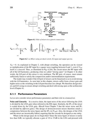
![Sec. 6.1. General Considerations 339
the design of the mixer, seeking to maximize its linearity while not raising its NF. If the
resulting mixer design is not satisfactory, some iteration becomes necessary. For example,
we may decide to further linearize the mixer even if the NF increases and compensate for
the higher noise by raising the LNA gain. We elaborate on these points in various design
examples in this chapter.
In direct-conversion receivers, the IP2 of the LNA/mixer cascade must be maximized.
In Section 6.4, we introduce methods of raising the IP2 in mixers. Also, as mentioned
in Chapter 4, the mixing spurs due to the LO harmonics become important in broadband
receivers.
For upconversion mixers, the noise proves somewhat critical only if the TX output
noise in the RX band must be very small (Chapter 4), but even such cases demand more
relaxed mixer noise performance than receivers do. The linearity of upconversion mixers
is specified by the type of modulation and the baseband signal swings.
Gain Downconversion mixers must provide sufficient gain to adequately suppress the
noise contributed by subsequent stages. However, low supply voltages make it difficult to
achieve a gain of more than roughly 10 dB while retaining linearity. Thus, the noise of
stages following the mixer still proves critical.
In direct-conversion transmitters, it is desirable to maximize the gain and hence the
output swings of upconversion mixers, thereby relaxing the gain required of the power
amplifier. In two-step transmitters, on the other hand, the IF mixers must provide only a
moderate gain so as to avoid compressing the RF mixer.
The gain of mixers must be carefully defined to avoid confusion. The “voltage con-
version gain” of a downconversion mixer is given by the ratio of the rms voltage of the IF
signal to the rms voltage of the RF signal. Note that these two signals are centered around
two different frequencies. The voltage conversion gain can be measured by applying a
sinusoid at ωRF and finding the amplitude of the downconverted component at ωIF. For
upconversion mixers, the voltage conversion gain is defined in a similar fashion but from
the baseband or IF port to the RF port.
In traditional RF and microwave design, mixers are characterized by a “power conver-
sion gain,” defined as the output signal power divided by the input signal power. But in
modern RF design, we prefer to employ voltage quantities because the input impedances
are mostly imaginary, making the use of power quantities difficult and unnecessary.
Port-to-Port Feedthrough Owing to device capacitances, mixers suffer from unwanted
coupling (feedthrough) from one port to another [Fig. 6.3(a)]. For example, if the mixer
RF
LO
IF
R
V
VLO
RF VIF
L
(a) (b)
Figure 6.3 (a) Feedthrough mechanisms in a mixer, (b) feedthrough paths in a MOS mixer.](https://image.slidesharecdn.com/rfmicroelectronicsrazavi-230814101614-71259b59/85/RF-MICROELECTRONICS_Razavi-pdf-364-320.jpg)
![340 Chap. 6. Mixers
LPF
LPF
LNA
LO
Figure 6.4 Effect of LO-RF feedthrough.
is realized by a MOSFET [Fig. 6.3(b)], then the gate-source and gate-drain capacitances
create feedthrough from the LO port to the RF and IF ports.
The effect of mixer port-to-port feedthrough on the performance depends on the
architecture. Consider the direct-conversion receiver shown in Fig. 6.4. As explained in
Chapter 4, the LO-RF feedthrough proves undesirable as it produces both offsets in the
baseband and LO radiation from the antenna. Interestingly, this feedthrough is entirely
determined by the symmetry of the mixer circuit and LO waveforms (Section 6.2.2). The
LO-IF feedthrough is benign because it is heavily suppressed by the baseband low-pass
filter(s).
Example 6.1
Consider the mixer shown in Fig. 6.5, where VLO 5 V1 cos ωLOt 1 V0 and CGS denotes the
gate-source overlap capacitance of M1. Neglecting the on-resistance of M1 and assuming
abrupt switching, determine the dc offset at the output for RS 5 0 and RS 0. Assume
RL RS.
R
VLO
V
L
RS
VRF
X
CGS
out
M 1
Figure 6.5 LO-RF feedthrough in a MOS device operating as a mixer.
Solution:
The LO leakage to node X is expressed as
VX 5
RSCGSs
RSCGSs 1 1
VLO, (6.1)](https://image.slidesharecdn.com/rfmicroelectronicsrazavi-230814101614-71259b59/85/RF-MICROELECTRONICS_Razavi-pdf-365-320.jpg)
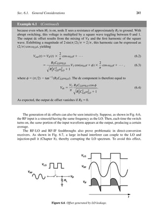
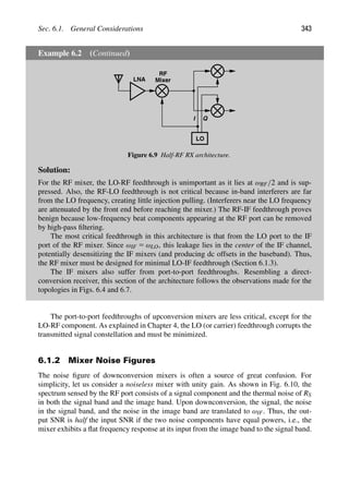
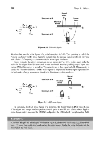
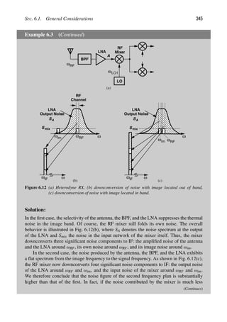
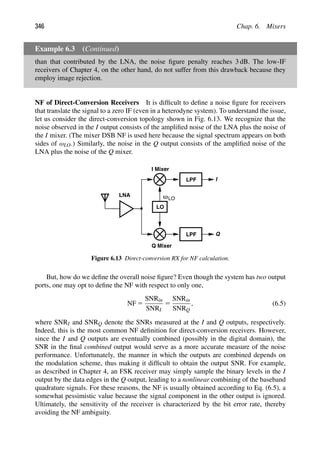
![Sec. 6.1. General Considerations 347
Example 6.4
Consider the simple mixer shown in Fig. 6.14(a). Assuming RL RS and the LO has a
50% duty cycle, determine the output noise spectrum due to RS, i.e., assume RL is noiseless.
R
t
(a)
R
S
V
2
n,RS
t
t
Vn,out
f
RS
kT
2
0 0
+3
+ f
fLO
fLO
−
fLO
fLO
−3
1
Vn,RS
(b)
f
RS
2kT
0
=
L
Figure 6.14 (a) Passive mixer, (b) input and output signals in time and frequency domains.
Solution:
Since Vout is equal to the noise of RS for half of the LO cycle and equal to zero for the
other half, we expect the output power density to be simply equal to half of that of the
input, i.e., V2
n,out 5 2kTRS. (This is the one-sided spectrum.) To prove this conjecture, we
view Vn,out(t) as the product of Vn,RS(t) and a square wave toggling between 0 and 1. The
output spectrum is thus obtained by convolving the spectra of the two [Fig. 6.14(b)]. It is
important to note that the power spectral density of the square wave has a sinc2
envelope,
exhibiting an impulse with an area of 0.52 at f 5 0, two with an area of (1/π)2 at f 5 ±fLO,
etc. The output spectrum consists of (a) 2kTRS 3 0.52, (b) 2kTRS shifted to the right and to
the left by ±fLO and multiplied by (1/π)2, (c) 2kTRS shifted to the right and to the left by
±3fLO and multiplied by [1/(3π)]2, etc. We therefore write
V2
n,out 5 2kTRS
1
22
1
2
π2
1
2
(3π)2
1
2
(5π)2
1 · · · (6.6)
5 2kTRS
1
22
1
2
π2
1 1
1
32
1
1
52
1 · · ·
. (6.7)
It can be proved that 122 1 322 1 522 1 · · · 5 π2/8. It follows that the two-sided output
spectrum is equal to kTRS and hence the one-sided spectrum is given by
V2
n,out 5 2kTRS. (6.8)](https://image.slidesharecdn.com/rfmicroelectronicsrazavi-230814101614-71259b59/85/RF-MICROELECTRONICS_Razavi-pdf-372-320.jpg)
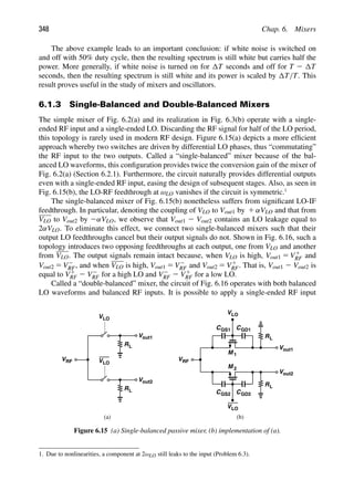
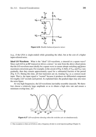
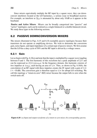
![Sec. 6.2. Passive Downconversion Mixers 351
Example 6.5
Explain why the mixer of Fig. 6.18 is ill-suited to direct-conversion receivers.
Solution:
Since the square wave toggling between 0 and 1 carries an average of 0.5, VRF itself also
appears at the output with a conversion gain of 0.5. Thus, low-frequency beat compo-
nents resulting from even-order distortion in the preceding stage directly go to the output,
yielding a low IP2.
Example 6.6
Determine the conversion gain if the circuit of Fig. 6.18(a) is converted to a single-balanced
topology.
Solution:
As illustrated in Fig. 6.19, the second output is similar to the first but shifted by 1808.
Thus, the differential output contains twice the amplitude of each single-ended output. The
conversion gain is therefore equal to 2/π ( ≈ 24 dB). Providing differential outputs and
twice the gain, this circuit is superior to the single-ended topology of Fig. 6.18(a).
R
VLO
V
L
out1
R
VLO
V
L
VRF
out2
t
Vout1 V
− out2
Figure 6.19 Waveforms for passive mixer gain computation.
Example 6.7
Determine the voltage conversion gain of a double-balanced version of the above topology
[Fig. 6.20(a)]. (Decompose the differential output to return-to-zero waveforms.)
(Continues)](https://image.slidesharecdn.com/rfmicroelectronicsrazavi-230814101614-71259b59/85/RF-MICROELECTRONICS_Razavi-pdf-376-320.jpg)
![Sec. 6.2. Passive Downconversion Mixers 353
CL
)
(t
x )
(t
y
LO
t
)
(t
y
)
(t
x
t t
)
(t
y
1
)
(t
y
2
(a)
(b)
Figure 6.21 (a) Sampling mixer, (b) output waveform decomposition.
where
[t/(T/2) 2 1/2] represents a square pulse with an amplitude of 1 between t 5 0
and t 5 T/2 and zero elsewhere. The right-hand side of Eq. (6.11) can also be expressed as
a sinc. Since y1(t) is equal to x(t) multiplied by a square wave toggling between zero and 1,
and since such a square wave is equal to the convolution of a square pulse and a train of
impulses [Fig. 6.22(a)], we have
y1(t) 5 x(t)
%
t
TLO/2
2
1
2
∗
1 ∞
k 5 2∞
δ (t 2 kTLO)
, (6.12)
0 0
(a)
(b)
t
1
T LO
t
1
0
=
t
0 TLO T LO
+ +2
TLO
T LO
−2 −
1
0
+3
+ f
f fLO
fLO
−
fLO
fLO
−3
f
IF Component
T LO
2
in )
(
Y1 f
Figure 6.22 (a) Decomposition of a square wave, (b) input and output spectra corresponding
to y1(t).](https://image.slidesharecdn.com/rfmicroelectronicsrazavi-230814101614-71259b59/85/RF-MICROELECTRONICS_Razavi-pdf-378-320.jpg)
![354 Chap. 6. Mixers
where TLO denotes the LO period. It follows from Eqs. (6.9) and (6.11) that
Y1( f) 5 X( f) ∗
1
jω
1 2 e2jωTLO/2
1
TLO
1 ∞
k 5 2∞
δ
f 2
k
TLO
. (6.13)
Figure 6.22(b) shows the corresponding spectra. The component of interest in Y1( f) lies at
the IF and is obtained by setting k to ±1:
Y1( f)|IF 5 X( f) ∗
1
jω
1 2 e2jωTLO/2
1
TLO
δ
f ±
1
TLO
. (6.14)
The impulse, in essence, computes [1/( jω)][1 2 exp(2jωTLO/2)] at ±1/TLO, which
amounts to ±TLO/( jπ). Multiplying this result by (1/TLO)δ( f ± 1/TLO) and convolving it
with X( f), we have
Y1( f)|IF 5
X( f 2 fLO)
jπ
2
X( f 1 fLO)
jπ
. (6.15)
As expected, the conversion gain from X( f) to Y1( f) is equal to 1/π, but with a phase shift
of 908.
The second output in Fig. 6.21(b), y2(t), can be viewed as a train of impulses that
sample the input and are subsequently convolved with a square pulse [Fig. 6.23(a)].
That is,
y2(t) 5
x(t)
1 ∞
k 5 2∞
δ
t 2 kTLO 2
TLO
2
∗
%
t
TLO/2
2
1
2
, (6.16)
t
)
(t
y
2
TLO
2
t
0
TLO
TLO
2
3 TLO
2 TLO
2
5 t
TLO
2
TLO
2
3 TLO
2
5 TLO
2
0 f
(a)
(b)
IF Component
in )
(
Y f
2
Figure 6.23 (a) Decomposition of y2(t), (b) corresponding spectrum.](https://image.slidesharecdn.com/rfmicroelectronicsrazavi-230814101614-71259b59/85/RF-MICROELECTRONICS_Razavi-pdf-379-320.jpg)
![Sec. 6.2. Passive Downconversion Mixers 355
and hence
Y2( f) 5
X( f) ∗
1
TLO
1 ∞
k 5 2∞
e2jωTLO/2
δ
f 2
k
TLO
·
1
jω
1 2 e2jωTLO/2
. (6.17)
Figure 6.23(b) depicts the spectrum, revealing that shifted replicas of X( f) are multiplied
by a sinc envelope. Note the subtle difference between Y1( f) and Y2( f): in the former, each
replica of X( f) is simply scaled by a factor, whereas in the latter, each replica experiences a
“droop” due to the sinc envelope. The component of interest in Y2( f) is obtained by setting
k to ±1:
Y2( f)|IF 5
1
TLO
[2X( f 2 fLO) 2 X( f 1 fLO)]
1
jω
1 2 e2jωTLO/2
. (6.18)
The term in the second set of square brackets must be calculated at the IF. If the IF is much
lower than 2fLO, then exp(2jωIFTLO/2) ≈ 1 2 jωIFTLO/2. Thus,
Y2( f)|IF ≈
2X( f 2 fLO) 2 X( f 1 fLO)
2
. (6.19)
Note that Y2( f) in fact contains a larger IF component than does Y1( f). The total IF output
is therefore equal to
|Y1( f) 1 Y2( f)|IF 5
1
π2
1
1
4
[|X( f 2 fLO)| 1 |X( f 1 fLO)|] (6.20)
5 0.593[|X( f 2 fLO)| 1 |X( f 1 fLO)|]. (6.21)
If realized as a single-balanced topology (Fig. 6.24), the circuit provides a gain twice this
value, 1.186 ≈ 1.48 dB. That is, a single-balanced sampling mixer exhibits about 5.5 dB
higher gain than its return-to-zero counterpart. It is remarkable that, though a passive cir-
cuit, the single-ended sampling mixer actually has a voltage conversion gain greater than
unity, and hence is a more attractive choice. The return-to-zero mixer is rarely used in
modern RF design.
VLO
Vout1
VLO
Vout2
CL
CL
in
V
Figure 6.24 Single-balanced sampling mixer.](https://image.slidesharecdn.com/rfmicroelectronicsrazavi-230814101614-71259b59/85/RF-MICROELECTRONICS_Razavi-pdf-380-320.jpg)
![356 Chap. 6. Mixers
Example 6.8
Determine the voltage conversion gain of a double-balanced sampling mixer.
Solution:
Shown in Fig. 6.25, such a topology operates identically to the counterpart in Fig. 6.20(a).
In other words, the capacitors play no role here because each output is equal to one of the
inputs at any given point in time. The conversion gain is therefore equal to 2/π, about
5.5 dB lower than that of the single-balanced topology of Fig. 6.24.
VLO
Vout1
VRF
Vout2
+
VRF
−
VLO
VLO
CL
CL
Figure 6.25 Double-balanced sampling mixer.
The above example may rule out the use of double-balanced sampling mixers. Since
most receiver designs incorporate a single-ended LNA, this is not a serious limitation.
However, if necessary, double-balanced operation can be realized through the use of two
single-balanced mixers whose outputs are summed in the current domain. Illustrated con-
ceptually in Fig. 6.26 [1], the idea is to retain the samples on the capacitors, convert each
differential output voltage to a current by means of M1–M4, add their output currents, and
VLO
VLO
in
V
+
VLO
VLO in
V
−
M 1 M 2 M M
3 4
VDD
Figure 6.26 Output combining of two single-balanced mixers in the current domain.](https://image.slidesharecdn.com/rfmicroelectronicsrazavi-230814101614-71259b59/85/RF-MICROELECTRONICS_Razavi-pdf-381-320.jpg)
![Sec. 6.2. Passive Downconversion Mixers 357
apply the currents to load resistors, thus generating an output voltage. In this case, the
mixer conversion gain is still equal to 1.48 dB.
6.2.2 LO Self-Mixing
Recall from Chapter 4 that the leakage of the LO waveform to the input of a mixer is added
to the RF signal and mixed with the LO, generating a dc offset at the output. We now study
this mechanism in the single-balanced sampling mixer. Consider the arrangement shown
in Fig. 6.27(a), where RS denotes the output impedance of the previous stage (the LNA).
Suppose the LO waveforms and the transistors are perfectly symmetric. Then, due to the
nonlinearity of CGS1 and CGS2 arising from large LO amplitudes, VP does change with time
but only at twice the LO frequency [Fig. 6.27(b)] (Problem 6.3). Upon mixing with the LO
signal, this component is translated to fLO and 3fLO—but not to dc. In other words, with
perfectly-symmetric devices and LO waveforms, the mixer exhibits no LO self-mixing and
hence no output dc offsets.
In practice, however, mismatches between M1 and M2 and within the oscillator circuit
give rise to a finite LO leakage to node P. Accurate calculation of the resulting dc offset is
difficult owing to the lack of data on various transistor, capacitor, and inductor mismatches
that lead to asymmetries. A rough rule of thumb is 10–20 millivolts at the output of the
mixer.
6.2.3 Noise
In this section, we study the noise behavior of return-to-zero and sampling mixers. Our
approach is to determine the output noise spectrum, compute the output noise power in
1 Hz at the IF, and divide the result by the square of the conversion gain, thus obtaining the
input-referred noise.
Let us begin with the RZ mixer, shown in Fig. 6.28. Here, Ron denotes the on-resistance
of the switch. We assume a 50% duty cycle for the LO. The output noise is given by
4kT(Ron||RL) when S1 is on and by 4kTRL when it is off. As shown in Example 6.4, on the
(b)
VLO
VLO
CGS1
M 1
Vout1
M 2
CGS2
Vout2
RS
VRF
t
VLO
VLO
P
VP
(a)
Figure 6.27 (a) LO-RF leakage path in a sampling mixer, (b) LO and leakage waveforms.](https://image.slidesharecdn.com/rfmicroelectronicsrazavi-230814101614-71259b59/85/RF-MICROELECTRONICS_Razavi-pdf-382-320.jpg)
![358 Chap. 6. Mixers
R
R
V
2
n,RS
Vn,out
S 1
on
L
V
2
n,RL
Figure 6.28 RZ mixer for noise calculation.
average, the output contains half of 4kT(Ron||RL) and half of 4kTRL:
V2
n,out 5 2kT[(Ron||RL) 1 RL]. (6.22)
If we select Ron RL so as to minimize the conversion loss, then
V2
n,out ≈ 2kTRL. (6.23)
Dividing this result by 1/π2, we have
V2
n,in ≈ 2π2
kTRL (6.24)
≈ 20kTRL. (6.25)
That is, the noise power of RL ( 5 4kTRL) is “amplified” by a factor of 5 when referred to
the input.
Example 6.9
If Ron 5 100 and RL 5 1 k, determine the input-referred noise of the above RZ mixer.
Solution:
We have
V2
n,in 5 8.14 nV/
√
Hz. (6.26)
This noise would correspond to a noise figure of 10 log[1 1 (8.14/0.91)2] 5 19 dB in a
50- system.
The reader may wonder if our choice Ron RL is optimum. If RL is very high, the
output noise decreases but so does the conversion gain. We now remove the assump-
tion Ron RL and express the voltage conversion gain as (1/π)RL/(Ron 1 RL). Dividing
Eq. (6.22) by the square of this value gives
V2
n,in 5 2π2
kT
(Ron 1 RL)(2Ron 1 RL)
RL
. (6.27)](https://image.slidesharecdn.com/rfmicroelectronicsrazavi-230814101614-71259b59/85/RF-MICROELECTRONICS_Razavi-pdf-383-320.jpg)
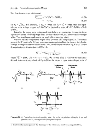
![360 Chap. 6. Mixers
R1 when S1 is on and a sampled, constant value when it is off. Third, in a manner similar
to the gain calculation in Fig. 6.21, we can decompose the output into two waveforms Vn1
and Vn2 as shown in Fig. 6.29(c).
It is tempting to consider the overall output spectrum as the sum of the spectra of Vn1
and Vn2. However, as explained below, the low-frequency noise components generated
by R1 create correlation between the track-mode and hold-mode noise waveforms. For
this reason, we proceed as follows: (1) compute the spectrum of Vn1 while excluding the
low-frequency components in the noise of R1, (2) do the same for Vn2, and (3) add the
contribution of the low-frequency components to the final result. In the derivations below,
we refer to the first two as simply the spectra of Vn1 and Vn2 even though Vn1(t) and
Vn2(t) in Fig. 6.29 are affected by the low-frequency noise of R1. Similarly, we use the
notation V2
n,LPF( f) even though its low-frequency components are removed and considered
separately.
Spectrum of Vn1 To calculate the spectrum of Vn1, we view this waveform as the product
of Vn,LPF(t) and a square wave toggling between 0 and 1. As shown in Fig. 6.30, the
spectrum of Vn1 is given by the convolution of V2
n,LPF( f) and the power spectral density of
the square wave (impulses with a sinc2 envelope). In practice, the sampling bandwidth of
the mixer, 1/(R1C1), rarely exceeds 3ωLO, and hence
V2
n1( f) 5 2 3
1
π2
1
1
9π2
2kTR1
1 1 (2πR1C1f)2
, (6.31)
where the factor of 2 on the right-hand side accounts for the aliasing of components at
negative and positive frequencies. At low output frequencies, this expression reduces to
V2
n1 5 0.226(2kTR1). (6.32)
Note that this is the two-sided spectrum of V2
n1.
0 f LO f LO
f
2kTR1
+
V
2
n,LPF
f
0
sinc
2
PSD of
Square Wave
Envelope
π2
1
1
9π2
f LO
−
f LO +3
−3
Figure 6.30 Aliasing in Vn1.
Spectrum of Vn2 The spectrum of Vn2 in Fig. 6.29(c) can be obtained using the approach
illustrated in Fig. 6.21 for the conversion gain. That is, Vn2 is equivalent to sampling Vn,LPF
by a train of impulses and convolving the result with a square pulse,
[t/(2TLO) 2 1/2].
We must therefore convolve the spectrum of Vn,LPF with a train of impulses (each having
an area of 1/T2
LO) and multiply the result by a sinc2 envelope. As shown in Fig. 6.31, the](https://image.slidesharecdn.com/rfmicroelectronicsrazavi-230814101614-71259b59/85/RF-MICROELECTRONICS_Razavi-pdf-385-320.jpg)
![Sec. 6.2. Passive Downconversion Mixers 361
0 f
f
0 LO fLO fLO
f
2kTR1
+ +2
fLO
fLO
fLO −2 −
V
2
n,LPF
Spectrum of
Impulse Train
+3
−3
Figure 6.31 Aliasing in Vn2.
convolution translates noise components around ±fLO, ±2fLO, etc., to the IF. The sum of
these aliased components is given by
V2
n,alias 5 2 3
2kTR1
T2
LO
1
1 1 4π2R2
1C2
1f2
LO
1
1
1 1 4π2R2
1C2
1 2f2
LO
1 · · ·
(6.33)
5 2 3
2kTR1
T2
LO
∞
n 5 1
1
1 1 a2n2
, (6.34)
where a 5 2πR1C1fLO. For the summation in Eq. (6.34), we have
∞
n 5 1
1
1 1 a2n2
5
1
2
π
a
coth
π
a
2 1
, (6.35)
Also, typically (2πR1C1)21
fLO and hence coth(2R1C1fLO)21 ≈ 1. It follows that
V2
n,alias 5
kT
T2
LO
1
C1fLO
2 2R1
. (6.36)
This result must be multiplied by the sinc2 envelope, |( jω)21[1 2 exp(2jωTLO/2)]|2,
which has a magnitude of T2
LO/4 at low frequencies. Thus, the two-sided IF spectrum of
Vn2 is given by
V2
n2 5 kT
1
4C1fLO
2
R1
2
. (6.37)
Correlation Between Vn1 and Vn2 We must now consider the correlation between Vn1
and Vn2 in Fig. 6.29. The correlation arises from two mechanisms: (1) as the circuit enters
the track mode, the previous sampled value takes a finite time to vanish, and (2) when the
circuit enters the hold mode, the frozen noise value, Vn2, is partially correlated with Vn1.
The former mechanism is typically negligible because of the short track time constant. For
the latter, we recognize that the noise frequency components far below fLO remain relatively
constant during the track and hold modes (Fig. 6.32); it is as if they experienced a zero-
order hold operation and hence a conversion gain of unity. Thus, the R1 noise components
from 0 to roughly fLO/10 directly appear at the output, adding a noise PSD of 2kTR1.
Summing the one-sided spectra of Vn1 and Vn2 and the low-frequency contribution,
4kTR1, gives the total (one-sided) output noise at the IF:
V2
n,out,IF 5 kT
3.9R1 1
1
2C1fLO
. (6.38)](https://image.slidesharecdn.com/rfmicroelectronicsrazavi-230814101614-71259b59/85/RF-MICROELECTRONICS_Razavi-pdf-386-320.jpg)
![362 Chap. 6. Mixers
t
Low−Frequency
Noise Noise
Sampled
TLO
2
TLO
TLO
2
3 TLO
2 TLO
2
5
0
Figure 6.32 Correlation between noise components in acquisition and hold modes.
R1
R1
Vout
Vin
R1
R1
Vn,out
(a) (b)
Figure 6.33 (a) Equivalent circuit of double-balanced passive mixer, (b) simplified circuit.
The input-referred noise is obtained by dividing this result by 1/π2 1 1/4:
V2
n,in 5 2.85kT
3.9R1 1
1
2C1fLO
. (6.39)
Note that [2] and [3] do not predict the dependence on R1 or C1.
For a single-balanced topology, the differential output exhibits a noise power twice
that given by Eq. (6.38), but the voltage conversion gain is twice as high. Thus, the input-
referred noise of a single-balanced passive (sampling) mixer is equal to
V2
n,in,SB 5
kT
2
1
π2
1
1
4
3.9R1 1
1
2C1fLO
(6.40)
5 1.42kT
3.9R1 1
1
2C1fLO
. (6.41)
Let us now study the noise of a double-balanced passive mixer. As mentioned in Exam-
ple 6.8, the behavior of the circuit does not depend much on the absence or presence of load
capacitors. With abrupt LO edges, a resistance equal to R1 appears between one input and
one output at any point in time [Fig. 6.33(a)]. Thus, from Fig. 6.33(b), V2
n,out 5 8kTR1.
Since the voltage conversion is equal to 2/π,
V2
n,in 5 2π2
kTR1. (6.42)](https://image.slidesharecdn.com/rfmicroelectronicsrazavi-230814101614-71259b59/85/RF-MICROELECTRONICS_Razavi-pdf-387-320.jpg)
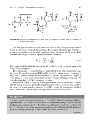
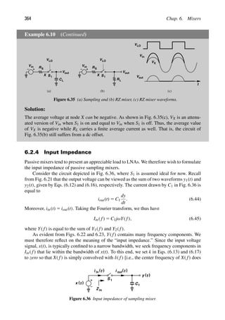
![Sec. 6.2. Passive Downconversion Mixers 365
not change]. (This stands in contrast to gain and noise calculations, where k was chosen to
translate X( f) to the IF of interest.) It follows that
Iin( f)
C1jω
5 X( f) ∗
1
jω
1 2 e2jωTLO/2
1
TLO
δ( f)
1
'
X( f) ∗
1
TLO
e2jωTLO/2
δ( f)
(
1
jω
1 2 e2jωTLO/2
. (6.46)
In the square brackets in the first term, ω must be set to zero to evaluate the impulse at
f 5 0. Thus, the first term reduces to (1/2)X( f). In the second term, the exponential in the
square brackets must also be calculated at ω 5 0. Consequently, the second term simplifies
to (1/TLO)X( f)[1/( jω)][12exp(2jωTLO/2)]. We then arrive at an expression for the input
admittance:
Iin( f)
X( f)
5 jC1ω
1
2
1
1
jωTLO
1 2 e2jωTLO/2
. (6.47)
Note that the on-resistance of the switch simply appears in series with the inverse of (6.47).
It is instructive to examine Eq. (6.47) for a few special cases. If ω (the input frequency)
is much less than ωLO, then the second term in the square brackets reduces to 1/2 and
Iin( f)
X( f)
5 jC1ω. (6.48)
In other words, the entire capacitance is seen at the input [Fig. 6.37(a)]. If ω ≈ 2πfLO (as in
direct-conversion receivers), then the second term is equal to 1/( jπ) and
Iin( f)
X( f)
5
jC1ω
2
1 2fC1. (6.49)
The input impedance thus contains a parallel resistive component equal to 1/(2fC1)
[Fig. 6.37(b)]. Finally, if ω 2πfLO, the second term is much less than the first, yielding
Iin( f)
X( f)
5
jC1ω
2
. (6.50)
For the input impedance of a single-balanced mixer, we must add the switch on-
resistance, R1, to the inverse of Eq. (6.47) and halve the result. If ω ≈ ωLO, then
Zin,SB 5
1
2
⎡
⎢
⎣R1 1
1
jC1ω
2
1 2fC1
⎤
⎥
⎦ . (6.51)
t
)
(t
y
C1
Z in
t
)
(t
y
C1
Z in
2 C1
2f
1
(a) (b)
Figure 6.37 Input impedance of passive mixer for (a) ω ωLO and (b) ω ≈ ωLO.](https://image.slidesharecdn.com/rfmicroelectronicsrazavi-230814101614-71259b59/85/RF-MICROELECTRONICS_Razavi-pdf-390-320.jpg)
![366 Chap. 6. Mixers
VLO
Z mix
Baseband
Amplifier
LNA
CBB
Figure 6.38 Baseband input capacitance reflected at the input of passive mixer.
Flicker Noise An important advantage of passive mixers over their active counterparts
is their much lower output flicker noise. This property proves critical in narrowband appli-
cations, where 1/f noise in the baseband can substantially corrupt the downconverted
channel.
MOSFETs produce little flicker noise if they carry a small current [4], a condition
satisfied in a passive sampling mixer if the load capacitance is relatively small. However,
the low gain of passive mixers makes the 1/f noise contribution of the subsequent stage
critical. Thus, the baseband amplifier following the mixer must employ large transistors,
presenting a large load capacitance to the mixer (Fig. 6.38). As explained above, CBB
manifests itself in the input impedance of the mixer, Zmix, thereby loading the LNA.
LO Swing Passive MOS mixers require large (rail-to-rail) LO swings, a disadvantage
with respect to active mixers. Since LC oscillators typically generate large swings, this is
not a serious drawback, at least at moderate frequencies (up to 5 or 10 GHz).
In Chapter 13, we present the design of a passive mixer followed by a baseband
amplifier for 11a/g applications.
6.2.5 Current-Driven Passive Mixers
The gain, noise, and input impedance analyses carried out in the previous sections have
assumed that the RF input of passive mixers is driven by a voltage source. If driven by a
current source, such mixers exhibit different properties. Figure 6.39(a) shows a conceptual
arrangement where the LNA has a relatively high output impedance, approximating a cur-
rent source. The passive mixer still carries no bias current so as to achieve low flicker noise
and it drives a general impedance ZBB. Voltage-driven and current-driven passive mixers
entail a number of interesting differences.
First, the input impedance of the current-driven mixer in Fig. 6.39 is quite different
from that of the voltage-driven counterpart. The reader may find this strange. Indeed, famil-
iar circuits exhibit an input impedance that is independent of the source impedance: we can
calculate the input impedance of an LNA by applying a voltage or a current source to the
input port. A passive mixer, on the other hand, does not satisfy this intuition because it is a
time-variant circuit. To determine the input impedance of a current-driven single-balanced
mixer, we consider the simplified case depicted in Fig. 6.39(b), where the on-resistance of
the switches is neglected. We wish to calculate Zin( f) 5 VRF( f)/Iin( f) in the vicinity of
the carrier (LO) frequency, assuming a 50% duty cycle for the LO.
The input current is routed to the upper arm for 50% of the time and flows through ZBB.
In the time domain [5],
V1(t) 5 [iin(t) 3 S(t)] ∗ h(t), (6.52)](https://image.slidesharecdn.com/rfmicroelectronicsrazavi-230814101614-71259b59/85/RF-MICROELECTRONICS_Razavi-pdf-391-320.jpg)
![Sec. 6.2. Passive Downconversion Mixers 367
LNA
VLO
VLO
M 1
M 2
Z in
Z BB
Z BB
C1
Vout
VLO
V
VLO
1
Z BB
Z BB
V2
1
2
S
S
I in VRF Z in
A
0 f
f
)
(
Iin f
c
+
fc
0 f
f
+
f LO
LO
−
−
0 f
Spectrum of
Downconverted Current
0 f
)
(f
1
V
Shape of
Z BB
)
(f
0 f
fc
+
fc
−
)
(f
1
V
Upconverted to RF
(a) (b)
(c)
Figure 6.39 (a) Current-driven passive mixer, (b) simplified model for input impedance calculation,
(c) spectra at input and output.
where S(t) denotes a square wave toggling between 0 and 1, and h(t) is the impulse response
of ZBB. In the frequency domain,
V1( f) 5 [Iin( f) ∗ S( f)] · ZBB( f), (6.53)
where S( f) is the spectrum of a square wave. As expected, upon convolution with the first
harmonic of S( f), Iin( f) is translated to the baseband and is then subjected to the frequency
response of ZBB( f). A similar phenomenon occurs in the lower arm.
We now make a critical observation [5]: the switches in Fig. 6.39(b) also mix the base-
band waveforms with the LO, delivering the upconverted voltages to node A. Thus, V1(t)
is multiplied by S(t) as it returns to the input, and its spectrum is translated to RF. The
spectrum of V2(t) is also upconverted and added to this result.
Figure 6.39(c) summarizes our findings, revealing that the downconverted spectrum
of Iin( f) is shaped by the frequency response of ZBB, and the result “goes back” through
the mixer, landing around fc while retaining its spectral shape. In other words, in response
to the spectrum shown for Iin( f), an RF voltage spectrum has appeared at the input that
is shaped by the baseband impedance. This implies that the input impedance around fc
resembles a frequency-translated version of ZBB( f). For example, if ZBB( f) is a low-pass
impedance, then Zin( f) has a band-pass behavior [5].
The second property of current-driven passive mixers is that their noise and nonlinear-
ity contribution are reduced [6]. This is because, ideally, a device in series with a current
source does not alter the current passing through it.](https://image.slidesharecdn.com/rfmicroelectronicsrazavi-230814101614-71259b59/85/RF-MICROELECTRONICS_Razavi-pdf-392-320.jpg)
![368 Chap. 6. Mixers
t
VLO,0
VLO,90
VLO,180
VLO,270
Figure 6.40 Quadrature LO waveforms with 25% duty cycle.
Passive mixers need not employ a 50% LO duty cycle. In fact, both voltage-driven and
current-driven mixers utilizing a 25% duty cycle provide a higher gain. Figure 6.40 shows
the quadrature LO waveforms according to this scenario. Writing the Fourier series for LO
waveforms having a duty cycle of d, the reader can show that the RF current entering each
switch generates an IF current given by [6]:
IIF(t) 5
2
π
sin πd
2d
IRF0 cos ωIFt, (6.54)
where IRF0 denotes the peak amplitude of the RF current. As expected, d 5 0.5 yields a gain
of 2/π. More importantly, for d 5 0.25, the gain reaches 2
√
2/π, 3 dB higher. Of course,
the generation of these waveforms becomes difficult at very high frequencies. [Ideally, we
would choose d ≈ 0 (impulse sampling) to raise this gain to unity.]
Another useful attribute of the 25% duty cycle in Fig. 6.40 is that the mixer switches
driven by LO0 and LO180 (or by LO90 and LO270) are not on simultaneously. As a result,
the mixer contributes smaller noise and nonlinearity [6].
6.3 ACTIVE DOWNCONVERSION MIXERS
Mixers can be realized so as to achieve conversion gain in one stage. Called active mixers,
such topologies perform three functions: they convert the RF voltage to a current, “com-
mutate” (steer) the RF current by the LO, and convert the IF current to voltage. These
operations are illustrated in Fig. 6.41. While both passive and active mixers incorporate
switching for frequency translation, the latter precede and follow the switching by voltage-
to-current (V/I) and current-to-voltage (I/V) conversion, respectively, thereby achieving
gain. We can intuitively observe that the input transconductance, IRF/VRF, and the out-
put transresistance, VIF/IIF, can, in principle, assume arbitrarily large values, yielding an
arbitrarily high gain.
Figure 6.42 depicts a typical single-balanced realization. Here, M1 converts the input
RF voltage to a current (and is hence called a “transconductor”), the differential pair M2–M3
commutates (steers) this current to the left and to the right, and R1 and R2 convert the output
currents to voltage. We call M2 and M3 the “switching pair.” As with our passive mixer
study in Section 6.2, we wish to quantify the gain, noise, and nonlinearity of this circuit.](https://image.slidesharecdn.com/rfmicroelectronicsrazavi-230814101614-71259b59/85/RF-MICROELECTRONICS_Razavi-pdf-393-320.jpg)
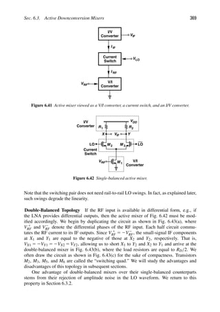
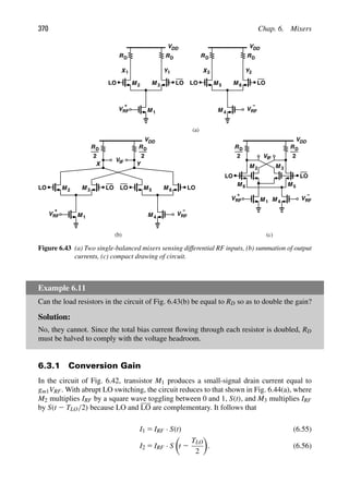
![Sec. 6.3. Active Downconversion Mixers 371
M 2 M 3
R
V
DD
R
out
1 2
I I
1 2
LO
LO
I RF g
= m1
VRF
(a) (b)
t
1
)
(
S t
t
1
)
(
S t
T LO
2
−
t
+1
−1
)
(
S t )
(
S t
T LO
2
−
−
Figure 6.44 (a) Equivalent circuit of active mixer, (b) switching waveforms.
Since Vout 5 VDD 2 I1R1 2 (VDD 2 I2R2), we have for R1 5 R2 5 RD,
Vout(t) 5 IRFRD S
t 2
TLO
2
2 S(t) . (6.57)
From Fig. 6.44(b), we recognize that the switching operation in Eq. (6.57) is equivalent to
multiplying IRF by a square wave toggling between 21 and 1 1. Such a waveform exhibits
a fundamental amplitude equal to 4/π,4
yielding an output given by
Vout(t) 5 IRF(t)RD ·
4
π
cos ωLOt 1 · · · . (6.58)
If IRF(t) 5 gm1VRF cos ωRFt, then the IF component at ωRF 2 ωLO is equal to
VIF(t) 5
2
π
gm1RDVRF cos(ωRF 2 ωLO)t. (6.59)
The voltage conversion gain is therefore equal to
VIF,p
VRF,p
5
2
π
gm1RD. (6.60)
What limits the conversion gain? We assume a given power budget, i.e., a certain
bias current, ID1, and show that the gain trades with the linearity and voltage headroom.
The input transistor is sized according to the overdrive voltage, VGS1 2 VTH1, that yields
the required IP3 (Chapter 5). Thus, VDS1,min 5 VGS1 2 VTH1. The transconductance of M1
is limited by the current budget and IP3, as expressed by gm1 5 2ID1/(VGS1 2 VTH1) [or
ID1/(VGS1 2 VTH1) for velocity-saturated devices]. Also, the value of RD is limited by
the maximum allowable dc voltage across it. In other words, we must compute the mini-
mum allowable value of VX and VY in Fig. 6.42. As explained in Section 6.3.3, linearity
4. It is helpful to remember that the peak amplitude of the first harmonic of a square wave is greater than the
peak amplitude of the square wave.](https://image.slidesharecdn.com/rfmicroelectronicsrazavi-230814101614-71259b59/85/RF-MICROELECTRONICS_Razavi-pdf-396-320.jpg)
![372 Chap. 6. Mixers
requirements dictate that M2 and M3 not enter the triode region so long as both carry
current.
Suppose the gate voltages of M2 and M3 in Fig. 6.42 are held at the common-mode level
of the differential LO waveforms, VCM,LO [Fig. 6.45(a)]. If M1 is at the edge of saturation,
then VN ≥ VGS1 2 VTH1:
VCM,LO 2 VGS2,3 ≥ VGS1 2 VTH1. (6.61)
Now consider the time instant at which the gate voltages of M2 and M3 reach VCM,LO 1 V0
and VCM,LO 2 V0, respectively, where V0 5
√
2(VGS2,3 2 VTH2)/2, a value high enough to
turn off M3 [Fig. 6.45(b)]. For M2 to remain in saturation up to this point, its drain voltage
must not fall below VCM,LO 1
√
2(VGS2,3 2 VTH2)/2 2 VTH2:
VX,min 5 VCM,LO 1
√
2
2
(VGS2,3 2 VTH2) 2 VTH2, (6.62)
which, from Eq. (6.61), reduces to
VX,min 5 VGS1 2 VTH1 1
1 1
√
2
2
(VGS2,3 2 VTH2). (6.63)
Thus, VX,min must accommodate the overdrive of M1 and about 1.7 times the “equilib-
rium” overdrive of each of the switching transistors. The maximum allowable dc voltage
across each load resistor is equal to
VR,max 5 VDD 2
VGS1 2 VTH1 1
1 1
√
2
2
(VGS2,3 2 VTH2)
. (6.64)
Since each resistor carries half of ID1,
RD,max 5
2VR,max
ID1
. (6.65)
RD
V
VDD
RD
M
M 1
2 M 3
IF
VRF
Y
X
V V
N
CM,LO
RD
V
VDD
RD
M
M 1
2 M 3
IF
VRF
Y
X
V
N
V +V0
V
V V0
−
(a) (b)
CM,LO
CM,LO
CM,LO
CM,LO
CM,LO
Figure 6.45 (a) Active mixer with LO at CM level, (b) required swing to turn one device off.](https://image.slidesharecdn.com/rfmicroelectronicsrazavi-230814101614-71259b59/85/RF-MICROELECTRONICS_Razavi-pdf-397-320.jpg)
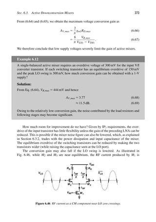
![374 Chap. 6. Mixers
split approximately equally between them, thus appearing as a common-mode current and
yielding little conversion gain for that period of time. Reduction of the LO swing tends to
increase this time and lower the gain (unless the LO is a square wave).
Example 6.13
Figure 6.47 shows a “dual-gate mixer,” where M1 and M2 can be viewed as one transistor
with two gates. Identify the drawbacks of this circuit.
VRF
RD
V
M
DD
M 1
V 2
LO
VIF
Figure 6.47 Dual-gate mixer.
Solution:
For M2 to operate as a switch, its gate voltage must fall to VTH2 above zero (why?) regard-
less of the overdrive voltages of the two transistors. For this reason, the dual-gate mixer
typically calls for larger LO swings than the single-balanced active topology does. Further-
more, since the RF current of M1 is now multiplied by a square wave toggling between 0
and 1, the conversion gain is half:
AV 5
1
π
gm1RD. (6.70)
Additionally, all of the frequency components produced by M1 appear at the output without
translation because they are multiplied by the average value of the square wave, 1/2. Thus,
half of the flicker noise of M1—a high-frequency device and hence small—emerges at IF.
Also, low-frequency beat components resulting from even-order distortion (Chapter 4) in
M1 directly corrupt the output, leading to a low IP2. The dual-gate mixer does not require
differential LO waveforms, a minor advantage. For these reasons, this topology is rarely
used in modern RF design.
With a sinusoidal LO, the drain currents of the switching devices depart from square
waves, remaining approximately equal for a fraction of each half cycle, T [Fig. 6.48(a)].
As mentioned previously, the circuit exhibits little conversion gain during these periods.
We now wish to estimate the reduction in the gain.](https://image.slidesharecdn.com/rfmicroelectronicsrazavi-230814101614-71259b59/85/RF-MICROELECTRONICS_Razavi-pdf-399-320.jpg)
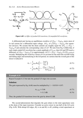
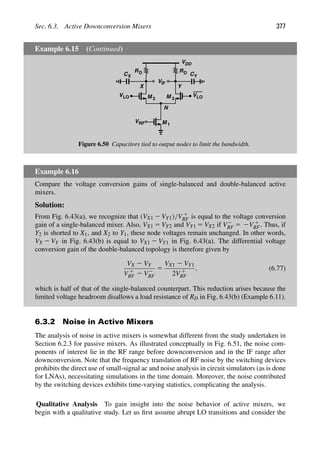
![378 Chap. 6. Mixers
RD
V
VDD
RD
M
M 1
2 M 3
IF
VRF
Y
X
VLO
VLO LO
RF
Noise
Noise
IF
P
Figure 6.51 Partitioning of active mixer for noise analysis.
RD
VDD
RD
M
M 1
2 M 3
VRF
VLO
VLO
P
CP
V
2
n,M2
M
M 1
2
CP
Vn,M2
CGS2
Vn,M2CPs
X
(a) (b)
P
I n=
Figure 6.52 (a) Effect of noise when one transistor is off, (b) equivalent circuit of (a).
representation in Fig. 6.52(a) for half of the LO cycle. Here,
CP 5 CGD1 1 CDB1 1 CSB2 1 CSB3 1 CGS3. (6.78)
In this phase, the circuit reduces to a cascode structure, with M2 contributing some noise
because of the capacitance at node P (Chapter 5). Recall from the analysis of cascode
LNAs in Chapter 5 that, at frequencies well below fT, the output noise current generated
by M2 is equal to Vn,M2CPs [Fig. 6.52(b)]. This noise and the noise current of M1 (which is
dominant) are multiplied by a square wave toggling between 0 and 1. Transistor M3 plays
an identical role in the next half cycle of the LO.
Now consider a more realistic case where the LO transitions are not abrupt, allowing
M2 and M3 to remain on simultaneously for part of the period. As depicted in Fig. 6.53, the
circuit now resembles a differential pair near equilibrium, amplifying the noise of M2 and
M3—while the noise of M1 has little effect on the output because it behaves as a common-
mode disturbance.](https://image.slidesharecdn.com/rfmicroelectronicsrazavi-230814101614-71259b59/85/RF-MICROELECTRONICS_Razavi-pdf-403-320.jpg)
![Sec. 6.3. Active Downconversion Mixers 379
RD
VDD
RD
M
M 1
2 M 3
VRF
V
V
V
2
n,M2 V
2
LO,CM LO,CM
n,M3
VIF
Figure 6.53 Effect of noise of M2 and M3 near equilibrium.
Example 6.17
Compare single-balanced and double-balanced active mixers in terms of their noise
behavior. Assume the latter’s total bias current is twice the former’s.
Solution:
Let us first study the output noise currents of the mixers [Fig. 6.54(a)]. If the total dif-
ferential output noise current of the single-balanced topology is I2
n,sing, then that of the
double-balanced circuit is equal to I2
n,doub 5 2I2
n,sing (why?). Next, we determine the output
noise voltages, bearing in mind that the load resistors differ by a factor of two [Fig. 6.54(b)].
We have
V2
n,out,sing 5 I2
n,sing(RD)2
(6.79)
V2
n,out,doub 5 I2
n,doub
RD
2
2
. (6.80)
But recall from Example 6.16 that the voltage conversion gain of the double-balanced mixer
is half of that of the single-balanced topology. Thus, the input-referred noise voltages of
the two circuits are related by
V2
n,in,sing 5
1
2
V2
n,in,doub. (6.81)
In this derivation, we have not included the noise of the load resistors. The reader can show
that Eq. (6.81) remains valid even with their noise taken into account. The single-balanced
mixer therefore exhibits less input noise and consumes less power.
(Continues)](https://image.slidesharecdn.com/rfmicroelectronicsrazavi-230814101614-71259b59/85/RF-MICROELECTRONICS_Razavi-pdf-404-320.jpg)
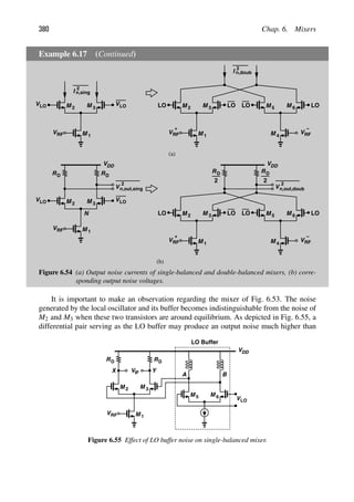
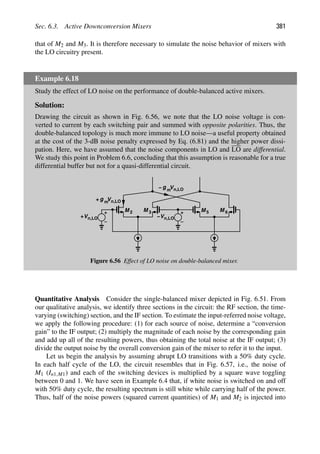
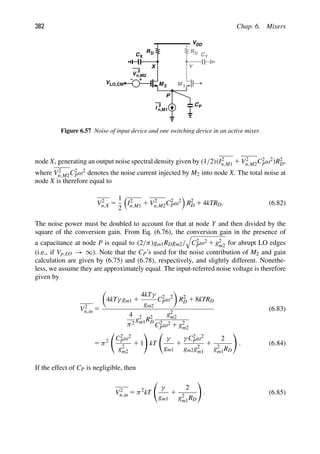
![Sec. 6.3. Active Downconversion Mixers 385
Flicker Noise Unlike passive mixers, active topologies suffer from substantial flicker
noise at their output, a serious issue if the IF signal resides near zero frequency and has a
narrow bandwidth.
Consider the circuit shown in Fig. 6.60(a). With perfect symmetry, the 1/f noise of ISS
does not appear at the output because it is mixed with ωLO (and its harmonics). Thus, only
the flicker noise of M2 and M3 must be considered. The noise of M2, V2
n2, experiences the
gain of the differential pair as it propagates to the output. Fortunately, the large LO swing
heavily saturates (desensitizes) the differential pair most of the time, thereby lowering the
gain seen by V2
n2.
In order to compute the gain experienced by Vn2 in Fig. 6.60(a), we assume a sinu-
soidal LO but also a small switching time for M2 and M3 such that ISS is steered almost
instantaneously from one to the other at the zero crossings of LO and LO [Fig. 6.60(b)].
How does Vn2 alter this behavior? Upon addition to the LO waveform, the noise modulates
the zero crossings of the LO [7]. This can be seen by computing the time at which the gate
voltages of M1 and M2 are equal; i.e., by equating the instantaneous gate voltages of M2
and M3:
VCM 1 Vp,LO sin ωLOt 1 Vn2(t) 5 VCM 2 Vp,LO sin ωLOt, (6.89)
obtaining
2Vp,LO sin ωLOt 5 2 Vn2(t). (6.90)
M 2 M 3
P
V
V
2
n2
I SS
V
RD
V
VDD
RD
IF
t
VLO
VLO
t
I D2
I D3
VLO
VLO
Vp,LO
t
ΔT
(a) (b) (c)
t
I D2
I D3
t
t
I D2 I D3
−
(d)
CM CM
Vn2
I SS
2
Figure 6.60 (a) Flicker noise of switching device, (b) LO and drain current waveforms, (c) modu-
lation of zero crossing due to flicker noise, (d) equivalent pulsewidth modulation.](https://image.slidesharecdn.com/rfmicroelectronicsrazavi-230814101614-71259b59/85/RF-MICROELECTRONICS_Razavi-pdf-410-320.jpg)
![386 Chap. 6. Mixers
In the vicinity of t 5 0, we have
2Vp,LOωLOt ≈ 2 Vn2(t). (6.91)
The crossing of LO and LO is displaced from its ideal point by an amount of T
(ωLO T 1 rad) [Fig. 6.60(c)]:
2Vp,LOωLO T ≈ 2 Vn2(t). (6.92)
That is,
| T| 5
|Vn2(t)|
2Vp,LOωLO
. (6.93)
Note that 2Vp,LOωLO is the slope of the differential LO waveform,5
SLO, and hence
| T| 5 |Vn2(t)|/SLO.
We now assume nearly abrupt drain current switching for M2 and M3 and consider
the above zero-crossing deviation as pulsewidth modulation of the currents [Fig. 6.60(d)].
Drawing the differential output current as in Fig. 6.60(d), we note that the modulated output
is equal to the ideal output plus a noise waveform consisting of a series of narrow pulses
of height 2ISS and width T and occurring twice per period [7]. If each narrow pulse is
approximated by an impulse, the noise waveform in ID2 2 ID3 can be expressed as
In,out(t) 5
1 ∞
k 5 2∞
2ISSVn2(t)
SLO
δ
t 2 k
TLO
2
. (6.94)
In the frequency domain, from Eq. (6.9),
In,out( f) 5
4ISS
TLOSLO
1 ∞
k 5 2∞
Vn2( f)δ(t 2 2kfLO). (6.95)
The baseband component is obtained for k 5 0 because Vn2( f) has a low-pass spectrum. It
follows that
In,out( f)|k 5 0 5
ISS
πVp,LO
Vn2( f), (6.96)
and hence
Vn,out( f)|k 5 0 5
ISSRD
πVp,LO
Vn2( f). (6.97)
In other words, the flicker noise of each transistor is scaled by a factor of ISSRD/(πVp,LO) as
it appears at the output. It is therefore desirable to minimize the bias current of the switching
devices. Note that this quantity must be multiplied by
√
2 to account for the flicker noise
of M3 as well.
5. Because the difference between VLO and VLO must reach zero in T seconds.](https://image.slidesharecdn.com/rfmicroelectronicsrazavi-230814101614-71259b59/85/RF-MICROELECTRONICS_Razavi-pdf-411-320.jpg)
![Sec. 6.3. Active Downconversion Mixers 387
Example 6.21
Refer the noise found above to the input of the mixer.
Solution:
Multiplying the noise by
√
2 to account for the noise of M3 and dividing by the conversion
gain, (2/π)gm1RD, we have
Vn,in( f)|k 5 0 5
√
2ISS
2gm1Vp,LO
Vn2( f) (6.98)
5
√
2(VGS 2 VTH)1
4Vp,LO
Vn2( f). (6.99)
For example, if (VGS 2 VTH)1 5 250 mV and Vp,LO 5 300 mV, then Vn2( f) is reduced by
about a factor of 3.4 when referred to the input. Note, however, that (1) Vn2( f) is typically
very large because M2 and M3 are relatively small, and (2) the noise voltage found above
must be multiplied by
√
2 to account for the noise of M3.
The above study also explains the low 1/f noise of passive mixers. Since ISS 5 0 in
passive topologies, a noise voltage source in series with the gate experiences a high atten-
uation as it appears at the output. (Additionally, MOSFETs carrying negligible current
produce negligible flicker noise.)
The reader may wonder if the above results apply to the thermal noise of M2 and M3
as well. Indeed, the analysis is identical [7] and the same results are obtained, with Vn2( f)
replaced with 4kTγ/gm2. The reader can show that this method and our earlier method of
thermal noise analysis yield roughly equal results if πVp,LO ≈ 5(VGS 2 VTH)eq2,3.
Another flicker noise mechanism in active mixers arises from the finite capacitance at
node P in Fig. 6.60(a) [7]. It can be shown that the differential output current in this case
includes a flicker noise component given by [7]
In,out( f) 5 2fLOCPVn2( f). (6.100)
Thus, a higher tail capacitance or LO frequency intensifies this effect. Nonetheless, the first
mechanism tends to dominate at low and moderate frequencies.
6.3.3 Linearity
The linearity of active mixers is determined primarily by the input transistor’s overdrive
voltage. As explained in Chapter 5, the IP3 of a common-source transistor rises with the
overdrive, eventually reaching a relatively constant value.
The input transistor imposes a direct trade-off between nonlinearity and noise because
IP3 ∝ VGS 2 VTH (6.101)
V2
n,in 5
4kTγ
gm
5
4kTγ
2ID
(VGS 2 VTH). (6.102)](https://image.slidesharecdn.com/rfmicroelectronicsrazavi-230814101614-71259b59/85/RF-MICROELECTRONICS_Razavi-pdf-412-320.jpg)
![388 Chap. 6. Mixers
RD
VDD
RD
M 1
M 3
VRF
Y
X
VLO
CY
I RF
CX
Ron2
I D2
P
Figure 6.61 Effect of output waveform on current steering when one device enters the triode region.
We also noted in Section 6.3.1 that the headroom consumed by the input transistor,
VGS 2 VTH, lowers the conversion gain [Eq. (6.67)]. Along with the above example, these
observations point to trade-offs among noise, nonlinearity, gain, and power dissipation in
active mixers.
The linearity of active mixers degrades if the switching transistors enter the triode
region. To understand this phenomenon, consider the circuit shown in Fig. 6.61, where M2
is in the triode region while M3 is still on and in saturation. Note that (1) the load resistors
and capacitors establish an output bandwidth commensurate with the IF signal, and (2) the
IF signal is uncorrelated with the LO waveform. If both M2 and M3 operate in saturation,
then the division of IRF between the two transistors is given by their transconductances and
is independent of their drain voltages.6
On the other hand, if M2 is in the triode region, then
ID2 is a function of the IF voltage at node X, leading to signal-dependent current division
between M2 and M3. To avoid this nonlinearity, M2 must not enter the triode region so long
as M3 is on and vice versa. Thus, the LO swings cannot be arbitrarily large.
Compression Let us now study gain compression in active mixers. The above effect
may manifest itself as the circuit approaches compression. If the output swings become
excessively large, the circuit begins to compress at the output rather than at the input, by
which we mean the switching devices introduce nonlinearity and hence compression while
the input transistor has not reached compression. This phenomenon tends to occur if the
gain of the active mixer is relatively high.
Example 6.22
An active mixer exhibits a voltage conversion gain of 10 dB and an input 1-dB compres-
sion point of 355 mVpp ( 5 25 dBm). Is it possible that the switching devices contribute
compression?
6. We neglect channel-length modulation here.](https://image.slidesharecdn.com/rfmicroelectronicsrazavi-230814101614-71259b59/85/RF-MICROELECTRONICS_Razavi-pdf-413-320.jpg)
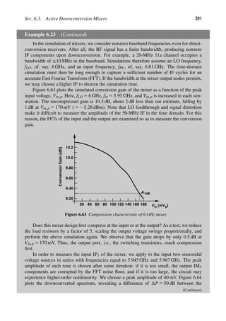
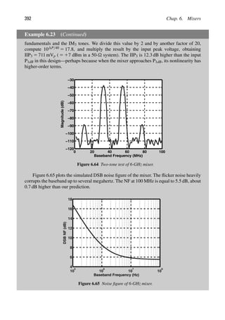
![Sec. 6.4. Improved Mixer Topologies 393
6.4 IMPROVED MIXER TOPOLOGIES
The mixer performance envelope defined by noise, nonlinearity, gain, power dissipation,
and voltage headroom must often be pushed beyond the typical scenarios studied thus far
in this chapter. For this reason, a multitude of circuit techniques have been introduced to
improve the performance of mixers, especially active topologies. In this section, we present
some of these techniques.
6.4.1 Active Mixers with Current-Source Helpers
The principal difficulty in the design of active mixers stems from the conflicting require-
ments between the input transistor current (which must be high enough to meet noise and
linearity specifications) and the load resistor current (which must be low enough to allow
large resistors and hence a high gain). We therefore surmise that adding current sources
(“helpers”) in parallel with the load resistors (Fig. 6.66) alleviates this conflict by affording
larger resistor values. If ID1 5 2I0 and each current source carries a fraction, αI0, then RD
can be as large as V0/[(1 2 α)I0], where V0 is the maximum allowable drop across RD [as
formulated by Eq. (6.64)]. Consequently, the voltage conversion gain rises as α increases.
For example, if α 5 0.5, then RD can be doubled and so can the gain. A higher RD also
reduces its input-referred noise contribution [Eq. (6.85)].
But how about the noise contributed by M4 and M5? Assuming that these devices are
biased at the edge of saturation, i.e., |VGS 2 VTH|4,5 5 V0, we write the noise current of
each as 4kTγ gm 5 4kTγ (2αI0)/V0, multiply it by R2
D to obtain the (squared) noise voltage
at each output node,8
and sum the result with the noise of RD itself:
V2
n,X 5 4kTγ
2αI0
V0
R2
D 1 4kTRD, (6.110)
where the noise due to other parts of the mixer is excluded. Since the voltage conversion
gain is proportional to RD, the above noise power must be normalized to R2
D [and eventually
V
M
M 1
2 M 3
IF
VRF
Y
VLO
VLO
Vb
Vb
VDD
I
2 0
I 0
α
X
RD R
I 0
α)
D
(1−
M M 5
4
Figure 6.66 Addition of load current sources to relax headroom constraints.
8. The output resistance of M4 and M5 can be absorbed in RD for this calculation.](https://image.slidesharecdn.com/rfmicroelectronicsrazavi-230814101614-71259b59/85/RF-MICROELECTRONICS_Razavi-pdf-418-320.jpg)
![394 Chap. 6. Mixers
the other factors in Eq. (6.85)]. We thus write
V2
n,X
R2
D
5 4kTγ
2αI0
V0
1
4kT
RD
(6.111)
5 4kT
I0
V0
(2αγ 1 1 2 α) (6.112)
5 4kT
I0
V0
[(2γ 2 1)α 1 1]. (6.113)
Interestingly, the total noise due to each current-source helper and its corresponding load
resistor rises with α, beginning from 4kTI0/V0 for α 5 0 and reaching (4kTI0/V0)(2γ ) for
α 5 1.
Example 6.24
Study the flicker noise contribution of M4 and M5 in Fig. 6.66.
Solution:
Modeled by a gate-referred voltage, V2
n,1/f , the flicker noise of each device is multiplied by
g2
m4,5R2
D as it appears at the output. As with the above derivation, we normalize this result
to R2
D:
V2
n,X
R2
D
5 V2
n,1/f
2αI0
V0
2
. (6.114)
Since the voltage headroom, V0, is typically limited to a few hundred millivolts, the helper
transistors tend to contribute substantial 1/f noise to the output, a serious issue in direct-
conversion receivers.
The addition of the helpers in Fig. 6.66 also degrades the linearity. In the calculations
leading to Eq. (6.113), we assumed that the helpers operate at the edge of saturation so as
to minimize their transconductance and hence their noise current, but this bias condition
readily drives them into the triode region in the presence of signals. The circuit is therefore
likely to compress at the output rather than at the input.
6.4.2 Active Mixers with Enhanced Transconductance
Following the foregoing thought process, we can insert the current-source helper in the RF
path rather than in the IF path. Depicted in Fig. 6.67 [8], the idea is to provide most of the
bias current of M1 by M4, thereby reducing the current flowing through the load resistors
(and the switching transistors). For example, if |ID4| 5 0.75ID1, then RD and hence the
gain can be quadrupled. Moreover, the reduction of the bias current switched by M2 and
M3 translates to a lower overdrive voltage and more abrupt switching, decreasing T in](https://image.slidesharecdn.com/rfmicroelectronicsrazavi-230814101614-71259b59/85/RF-MICROELECTRONICS_Razavi-pdf-419-320.jpg)
![Sec. 6.4. Improved Mixer Topologies 395
RD
V
VDD
RD
M
M 1
2 M 3
IF
VRF
Y
X
VLO
VLO
Vb
M
α)
(1− I D1
P
I
α D1
4
CP
Figure 6.67 Addition of current source to tail of switching pair.
Figs. 6.48(a) and 6.58 and lessening the gain and noise effects formulated by Eqs. (6.72)
and (6.88). Finally, the output flicker noise falls (Problem 6.10).
The above approach nonetheless faces two issues. First, transistor M4 contributes
additional capacitance to node P, exacerbating the difficulties mentioned earlier. As a
smaller bias current is allocated to M2 and M3, raising the impedance seen at their source
[ ≈ 1/(2gm)], CP “steals” a greater fraction of the RF current generated by M1, reducing
the gain. Second, the noise current of M4 directly adds to the RF signal. We can readily
express the noise currents of M1 and M4 as
I2
n,M1 1 I2
n,M4 5 4kTγ gm1 1 4kTγ gm4 (6.115)
5 4kTγ
2ID1
(VGS 2 VTH)1
1
2αID1
|VGS 2 VTH|2
. (6.116)
Example 6.25
A student eager to minimize the noise of M4 in the above equation selects |VGS 2 VTH|2 5
0.75 V with VDD 5 1 V. Explain the difficulty here.
Solution:
The bias current of M4 must be carefully defined so as to track that of M1. Poor match-
ing may “starve” M2 and M3, i.e., reduce their bias currents considerably, creating a high
impedance at node P and forcing the RF current to ground through CP. Now, consider the
simple current mirror shown in Fig. 6.68. If |VGS 2VTH|4 5 0.75 V, then |VGS4| may exceed
VDD, leaving no headroom for IREF. In other words, |VGS 2 VTH|4 must be chosen less than
VDD 2 |VGS4| 2 VIREF, where VIREF denotes the minimum acceptable voltage across IREF.
(Continues)](https://image.slidesharecdn.com/rfmicroelectronicsrazavi-230814101614-71259b59/85/RF-MICROELECTRONICS_Razavi-pdf-420-320.jpg)
![396 Chap. 6. Mixers
Example 6.25 (Continued)
VDD
M
M 1
2 M 3
VRF
P
I
M
M 4 REF
REF
Figure 6.68 Current mirror voltage limitations.
In order to suppress the capacitance and noise contribution of M4 in Fig. 6.68, an
inductor can be placed in series with its drain. Illustrated in Fig. 6.69(a) [9], such an
arrangement not only enhances the input transconductance but allows the inductor to res-
onate with CP. Additionally, capacitor C1 acts as a short at RF, shunting the noise current
of M4 to ground. As a result, most of the RF current produced by M1 is commutated by M2
and M3, and the noise injected by M2 and M3 is also reduced (because they switch more
abruptly).
In the circuit of Fig. 6.69(a), the inductor parasitics must be managed carefully. First,
L1 contributes some capacitance to node P, equivalently raising CP. Second, the loss of
L1 translates to a parallel resistance, “wasting” the RF current and adding noise. Depicted
in Fig. 6.69(b), this resistance, R1, must remain much greater than 1/(2gm2,3) so as to
RD
V
VDD
RD
M
M 1
2 M 3
IF
VRF
Y
X
VLO
VLO
Vb
M
P
4
L1
CP C1
N
M
M 1
2 M 3
VRF
VLO
VLO
P L1
R1
g
R
2 m2,3
1
1
(a) (b)
Figure 6.69 (a) Use of inductive resonance at tail with helper current source, (b) equivalent circuit
of inductor.](https://image.slidesharecdn.com/rfmicroelectronicsrazavi-230814101614-71259b59/85/RF-MICROELECTRONICS_Razavi-pdf-421-320.jpg)
![Sec. 6.4. Improved Mixer Topologies 397
negligibly shunt the RF current. Also, its noise current must be much less than that of M1.
Thus, the choice of the inductor is governed by the following conditions:
L1CP,tot 5
1
ω2
RF
(6.117)
R1 5 QL1ωRF
1
gm2,3
(6.118)
4kT
R1
5
4kT
QL1ωRF
4kTγ gm1, (6.119)
where CP,tot includes the capacitance of L1.
The circuits of Figs. 6.67 and 6.69 suffer from a drawback in deep-submicron tech-
nologies: since M1 is typically a small transistor, it poorly matches the current mirror
arrangement that feeds M4. As a result, the exact current flowing through the switching
pair may vary considerably.
Figure 6.70 shows another topology wherein capacitive coupling permits independent
bias currents for the input transistor and the switching pair [10]. Here, C1 acts as a short
circuit at RF and L1 resonates with the parasitics at nodes P and N. Furthermore, the voltage
headroom available to M1 is no longer constrained by (VGS 2 VTH)2,3 and the drop across
the load resistors. In a typical design, ID1/I0 may fall in the range of 3 to 5 for optimum
performance. Note that if I0 is excessively low, the switching pair does not absorb all of
the RF current. Another important attribute is that, as formulated by Eq. (6.97), a smaller
I0 leads to lower flicker noise at the output.
RD
V
VDD
RD
M
M 1
2 M 3
IF
VRF
Y
X
VLO
VLO
P
CP
L1
C1
I
CN
N
0
Figure 6.70 Active mixer using capacitive coupling with resonance.
6.4.3 Active Mixers with High IP2
As explained in Chapter 4, the second intercept point becomes critical in direct-conversion
and low-IF receivers as it signifies the corruption introduced by the beating of two
interferers or envelope demodulation of one interferer. We also noted that capacitive](https://image.slidesharecdn.com/rfmicroelectronicsrazavi-230814101614-71259b59/85/RF-MICROELECTRONICS_Razavi-pdf-422-320.jpg)
![Sec. 6.4. Improved Mixer Topologies 399
this result agrees with Eq. (6.97) because the offset can be considered a very slow noise
component.
An interesting observation offered by the output 1/f noise and offset equations is as
follows. If the bias current of the switching pair is reduced but that of the input transcon-
ductor is not, then the performance improves because the gain does not change but the
output 1/f noise and offset fall. For example, the current helpers described in the previous
section prove useful here.
We now replace ISS with a transconductor device as depicted in Fig. 6.71(d) and assume
VRF 5 Vm cos ω1t 1 Vm cos ω2t 1 VGS0, (6.120)
where VGS0 is the bias gate-source voltage of M1. With a square-law device, the IM2
product emerges in the current of M1 as
IIM2 5
1
2
μnCox
W
L
V2
m cos(ω1 2 ω2)t. (6.121)
Multiplying this quantity by VOSRD/(πVp,LO) yields the direct feedthrough to the output:
VIM2,out 5
1
2
μnCox
W
L
V2
m cos(ω1 2 ω2)t
VOSRD
πVp,LO
. (6.122)
To calculate the IP2, the value of Vm must be raised until the amplitude of VIM2,out becomes
equal to the amplitude of the main downconverted components. This amplitude is simply
given by (2/π)gm1RDVm. Thus,
1
2
μnCox
W
L
V2
IIP2
VOSRD
πVp,LO
5
2
π
gm1RDVIIP2. (6.123)
Writing gm1 as μnCox(W/L)(VGS 2 VTH)1, we finally obtain
VIIP2 5 4(VGS 2 VTH)1
Vp,LO
VOS
. (6.124)
For example, if (VGS 2 VTH)1 5 250 mV, Vp,LO 5 300 mV, and VOS 5 10 mV, then
VIIP2 5 30 VP ( 5 39.5 dBm in a 50- system). Other IP2 mechanisms are described
in [12].
The foregoing analysis also applies to asymmetries in the LO waveforms that would
arise from mismatches within the LO circuitry and its buffer. If the duty cycle is denoted
by (TLO/2 2 T)/TLO (e.g., 48%), then the dc component in ID1 2 ID2 is equal to
(2 T/TLO)ISS, yielding an average of (2 T/TLO)ISSRD at the output. We therefore replace
ISS with the IM2 component given by Eq. (6.121), arriving at
VIM2,out 5
1
2
μnCox
W
L
V2
m cos(ω1 2 ω2)t
2 T
TLO
RD. (6.125)](https://image.slidesharecdn.com/rfmicroelectronicsrazavi-230814101614-71259b59/85/RF-MICROELECTRONICS_Razavi-pdf-424-320.jpg)
![Sec. 6.4. Improved Mixer Topologies 401
Example 6.26 (Continued)
The cubic term in the square brackets produces an IM2 component if Vin 5 Vm cos ω1t 1
Vm cos ω2t because the term 3 V2
inVOS1 leads to the cross product of the two sinusoids:
VIM2 5
3[μnCox(W/L)]3/2
8
√
ISS
V2
mVOS1 cos(ω1 2 ω2)t (6.129)
5
3ISS
8(VGS 2 VTH)3
eq
V2
mVOS1 cos(ω1 2 ω2)t, (6.130)
where (VGS 2 VTH)eq represents the equilibrium overdrive of each transistor. Of course,
only a small fraction of this component appears at the output of the mixer. For example, if
only the offset of the switching quad, VOS2, is considered,9
then the IM2 amplitude must be
multiplied by VOS2RD/(πVp,LO), yielding an IIP2 of
VIIP2 5
16(VGS 2 VTH)2
eqVp,LO
3VOS1VOS2
. (6.131)
For example, if (VGS2VTH)eq 5 250 mV, Vp,LO 5 300 mV, and VOS1 5 VOS2 5 10 mV, then
VIIP2 5 1000 Vp ( 5 1 70 dBm in a 50- system).
While improving the IP2 significantly, the use of a differential pair in Fig. 6.72 degrades
the IP3. As formulated in Chapter 5, a quasi-differential pair (with the sources held at
ac ground) exhibits a higher IP3. We now repeat the calculations leading to Eq. (6.131)
for such a mixer (Fig. 6.73), noting that the input pair now has poor common-mode
VDD
M
M 1
M
VRF
+
M M
VRF
M
−
5 6
V
LO LO LO LO
R
RD D
2
3 4
VOS1
VOS2 VOS3
out
I I D2
D1
Figure 6.73 Effect of offsets in a double-balanced mixer using a quasi-differential input pair.
9. In this case, VOS2 represents the difference between the offsets of M3–M4 and M5–M6.](https://image.slidesharecdn.com/rfmicroelectronicsrazavi-230814101614-71259b59/85/RF-MICROELECTRONICS_Razavi-pdf-426-320.jpg)
![402 Chap. 6. Mixers
rejection. Let us apply V 1
RF 5 Vm cos ω1t 1 Vm cos ω2t 1 VGS0 and V2
RF 5 2 Vm cos ω1t 2
Vm cos ω2t 1 VGS0, obtaining
ID1 5
1
2
μnCox
W
L
1
(Vm cos ω1t 1 Vm cos ω2t 1 VOS1 1 VGS0 2 VTH)2
(6.132)
ID2 5
1
2
μnCox
W
L
2
(Vm cos ω1t 1 Vm cos ω2t 1 VGS0 2 VTH)2
. (6.133)
While independent of VOS1, the low-frequency beat in ID1 is multiplied by a factor of
VOS2RD/(πVp,LO) and that in ID2 by VOS3RD/(πVp,LO). Here, VOS2 and VOS3 denote the
offsets of M3–M4 and M5–M6, respectively. The output thus exhibits an IM2 component
given by
VIM2,out 5
1
2
μnCox
W
L
V2
m cos(ω1 2 ω2)t
RD
πVp,LO
(VOS2 1 VOS3). (6.134)
Noting that the output amplitude of each fundamental is equal to (2/π)2Vmgm1RD and that
gm1 5 μnCox(W/L)1(VGS0 2 VTH), we have
VIIP2 5
8(VGS0 2 VTH)
VOS2 1 VOS3
Vp,LO. (6.135)
For example, if VGS 2VTH 5 250 mV, Vp,LO 5 300 mV, and VOS2 5 VOS3 5 1 10 mV, then
VIIP2 5 30 Vp ( 5 1 39.5 dBm in a 50- system). Comparison of the IIP2’s obtained for the
differential and quasi-differential mixers indicates that the latter is much inferior, revealing
a trade-off between IP2 and IP3.
We have thus far considered one mechanism leading to a finite IP2: the passage of the
low-frequency beat through the mixer’s switching devices. On the other hand, even with
no even-order distortion in the transconductor, it is still possible to observe a finite low-
frequency beat at the output if (a) the switching devices (or the LO waveforms) exhibit
asymmetry and (b) a finite capacitance appears at the common source node of the switch-
ing devices [11, 12]. In this case, two interferers, Vm cos ω1t 1 Vm cos ω2t, arriving at the
common source node experience nonlinearity and mixing with the LO harmonics, thereby
generating a component at ω1 2 ω2 after downconversion. The details of this mechanism
are described in [11, 12].
While conceived for noise and gain optimization reasons, the mixer topology in
Fig. 6.70 also exhibits a high IP2. The high-pass filter consisting of L1, C1, and the resis-
tance seen at node P suppresses low-frequency beats generated by the even-order distortion
in M1. From the equivalent circuit shown in Fig. 6.74, we have
Im
Ibeat
5
L1s
L1s 1
1
C1s
1
1
2gm
(6.136)
5
L1C1s2
L1C1s2
1
C1s
2gm
1 1
. (6.137)](https://image.slidesharecdn.com/rfmicroelectronicsrazavi-230814101614-71259b59/85/RF-MICROELECTRONICS_Razavi-pdf-427-320.jpg)
![Sec. 6.4. Improved Mixer Topologies 403
RD
V
VDD
RD
M 2 M 3
IF Y
X
VLO
VLO
P
L1
I
I beat
SS
g
2
1
m
C1 I m
Figure 6.74 Effect of low-frequency beat in a mixer using capacitive coupling and resonance.
At low frequencies, this result can be approximated as
Im
Ibeat
≈ L1C1s2
, (6.138)
revealing a high attenuation.
Another approach to raising the IP2 is to degenerate the transconductor capacitively.
As illustrated in Fig. 6.75 [10], the degeneration capacitor, Cd, acts as a short circuit
at RF but nearly an open circuit at the low-frequency beat components. Expressing the
transconductance of the input stage as
Gm 5
gm1
1 1
gm1
Cds
(6.139)
5
gm1Cds
Cds 1 gm1
, (6.140)
we recognize that the gain at low frequencies falls in proportion to Cds, making M1
incapable of generating second-order intermodulation components.
M
M 1
2 M 3
VRF
VLO
VLO
I Cd
1
Figure 6.75 Effect of capacitive degeneration on IP2.](https://image.slidesharecdn.com/rfmicroelectronicsrazavi-230814101614-71259b59/85/RF-MICROELECTRONICS_Razavi-pdf-428-320.jpg)
![404 Chap. 6. Mixers
Example 6.27
The mixer of Fig. 6.75 is designed for a 900-MHz GSM system. What is the worst-case
attenuation that capacitive degeneration provides for IM2 products that would otherwise be
generated by M1? Assume a low-IF receiver (Chapter 4).
Solution:
We must first determine the worst-case scenario. We may surmise that the highest beat
frequency experiences the least attenuation, thereby creating the largest IM2 product. As
depicted in Fig. 6.76(a), this situation arises if the two interferers remain within the GSM
band (so that they are not attenuated by the front-end filter) but as far from each other as
possible, i.e., at a frequency difference of 25 MHz. Let us assume that the pole frequency,
gm/Cd, is around 900 MHz. The IM2 product therefore falls at 25 MHz and, therefore,
experiences an attenuation of roughly 900 MHz/25 MHz 5 36 ( ≈ 31 dB) by capacitive
degeneration. However, in a low-IF receiver, the downconverted 200-kHz GSM channel is
located near zero frequency. Thus, this case proves irrelevant.
0
GSM RX band
25 MHz
25 MHz f 0
25 MHz
25 MHz f
200 kHz
Desired
Channel
(a) (b)
Figure 6.76 Beat generation from (a) two blockers near the edges of GSM band, (b) two closely-
spaced blockers in GSM band.
From the above study, we seek two interferers that bear a frequency difference of 200
kHz (i.e., adjacent channels). As shown in Fig. 6.76(b), we place the adjacent interferers
near the edge of the GSM band. Located at a center frequency of 200 kHz, the beat experi-
ences an attenuation of roughly 935 MHz/200 kHz 5 4, 675 ≈ 73 dB. It follows that very
high IP2’s can be obtained for low-IF 900-MHz GSM receivers.
As mentioned earlier, even with capacitive coupling between the transconductor stage
and the switching devices, the capacitance at the common source node of the switching
pair ultimately limits the IP2 (if the offset of the switching pair is considered). We therefore
expect a higher IP2 if an inductor resonates with this capacitance. Figure 6.77 shows a
double-balanced mixer employing both capacitive degeneration and resonance to achieve
an IP2 of 1 78 dBm [11].](https://image.slidesharecdn.com/rfmicroelectronicsrazavi-230814101614-71259b59/85/RF-MICROELECTRONICS_Razavi-pdf-429-320.jpg)
![Sec. 6.4. Improved Mixer Topologies 405
M
M 1
2 M 3
VRF
+
M M
VRF
M
−
4
5 6
LO LO LO LO
L1
C1 C2
Figure 6.77 Use of inductor at sources of switching quad to raise IP2.
6.4.4 Active Mixers with Low Flicker Noise
Our study of noise in Section 6.3.2 revealed that the downconverted flicker noise of the
switching devices is proportional to their bias current and the parasitic capacitance at their
common source node. Since these trends also hold for the IP2 of active mixers, we postulate
that the techniques described in Section 6.4.3 for raising the IP2 lower flicker noise as
well. In particular, the circuit topologies in Figs. 6.69 and 6.74 both allow a lower bias
current for the switching pair and cancel the tail capacitance by the inductor. This approach,
however, demands two inductors (one for each quadrature mixer), complicating the layout
and routing.
Let us return to the helper idea shown in Fig. 6.67 and ask, is it possible to turn on the
helper only at the time when it is needed? In other words, can we turn on the PMOS current
source only at the zero crossings of the LO so that it lowers the bias current of the switching
devices and hence the effect of their flicker noise [13]? In such a scheme, the helper itself
would inject only common-mode noise because it turns on only when the switching pair is
in equilibrium.
Figure 6.78 depicts our first attempt in realizing this concept. Since large LO swings
produce a reasonable voltage swing at node P at 2ωLO, the diode-connected transistor turns
on when LO and LO cross and VP falls. As LO or LO rises, so does VP, turning MH off.
Thus, MH can provide most of the bias current of M1 near the crossing points of LO and
LO while injecting minimal noise for the rest of the period.
M
M 1
2 M 3
VRF
P
VDD
M H
LO LO
Figure 6.78 Use of a diode-connected device to reduce switching pair current.](https://image.slidesharecdn.com/rfmicroelectronicsrazavi-230814101614-71259b59/85/RF-MICROELECTRONICS_Razavi-pdf-430-320.jpg)
![406 Chap. 6. Mixers
Unfortunately, the diode-connected transistor in Fig. 6.78 does not turn off abruptly as
LO and LO depart from their crossing point. Consequently, MH continues to present a low
impedance at node P, shunting the RF current to ac ground. This issue can be resolved in
a double-balanced mixer by reconfiguring the diode-connected devices as a cross-coupled
pair [13]. As illustrated in Fig. 6.79 [13], MH1 and MH2 turn on and off simultaneously
because VP and VQ vary identically—as if MH1 and MH2 were diode-connected devices.
Thus, these two transistors provide most of the bias currents of M1 and M4 at the crossing
points of LO and LO. On the other hand, as far as the differential RF current of M1 and
M4 is concerned, the cross-coupled pair acts as a negative resistance (Chapter 8), partially
cancelling the positive resistance presented by the switching pairs at P and Q. Thus, MH1
and MH2 do not shunt the RF current.
M
M 1
2 M 3
VRF
+
M M
VRF
M
−
4
5 6
LO LO LO LO
Q
P
VDD
M
M H1 H2
Figure 6.79 Use of cross-coupled pair to reduce current of switching quad.
The circuit of Fig. 6.79 nonetheless requires large LO swings to ensure that VP and
VQ rise rapidly and sufficiently so as to turn off MH1 and MH2.10
Otherwise, these two
devices continue to inject differential noise for part of the period. Another drawback of this
technique is that it does not lend itself to single-balanced mixers.
Example 6.28
The positive feedback around MH1 and MH2 in Fig. 6.79 may cause latchup, i.e., a slight
imbalance between the two sides may pull P (or Q) toward VDD, turning MH2 (or MH1) off.
Derive the condition necessary to avoid latchup.
Solution:
The impedance presented by the switching pairs at P and Q is at its highest value when
either transistor in each differential pair is off (why?). Shown in Fig. 6.80 is the resulting
worst case. For a symmetric circuit, the loop gain is equal to (gmH/gm2,5)2, where gmH
10. Note that MH1 and MH2 do not help the switching of the differential pairs because the 2ωLO waveforms at
P and Q are identical (rather than differential).](https://image.slidesharecdn.com/rfmicroelectronicsrazavi-230814101614-71259b59/85/RF-MICROELECTRONICS_Razavi-pdf-431-320.jpg)
![Sec. 6.4. Improved Mixer Topologies 407
Example 6.28 (Continued)
represents the transconductance of MH1 and MH2. To avoid latchup, we must ensure that
gmH
gm2
2
1. (6.141)
VDD
M
M H1 H2
g
1
m2
g
1
P Q
m5
Figure 6.80 Equivalent circuit for latchup calculation.
The notion of reducing the current through the switching devices at the crossing points
of LO and LO can alternatively be realized by turning off the transconductor momentarily
[14]. Consider the circuit shown in Fig. 6.81(a), where switch S1 is driven by a waveform
having a frequency of 2fLO but a duty cycle of, say, 80%. As depicted in Fig. 6.81(b), S1
M
M 1
2 M 3
VRF
VLO
VLO
I D2 I D3
1
S
f
2 LO
I P
t
I D1
t
t
VLO
VLO
f
2 LO
t
I P
t
I D2
(a) (b)
Figure 6.81 (a) Use of a switch to turn off the switching pair near LO zero crossings, (b) circuit
waveforms.](https://image.slidesharecdn.com/rfmicroelectronicsrazavi-230814101614-71259b59/85/RF-MICROELECTRONICS_Razavi-pdf-432-320.jpg)
![408 Chap. 6. Mixers
briefly turns the transconductor off twice per LO period. Thus, if the crossing points of LO
and LO are chosen to fall at the times when IP is zero, then the flicker noise of M2 and
M3 is heavily attenuated. Moreover, M2 and M3 inject no thermal noise to the output near
the equilibrium. The concept can be extended to quadrature double-balanced mixers [14].
In Problem 6.12, we decide whether this circuit can also be viewed as a differential pair
whose current is modulated (chopped) at a rate of 2fLO.
The above approach entails a number of issues. First, the turn-off time of the transcon-
ductor must be sufficiently long and properly phased with respect to LO and LO so that
it encloses the LO transitions. Second, at high frequencies it becomes difficult to generate
2fLO with such narrow pulses; the conversion gain thus suffers because the transconductor
remains off for a greater portion of the period. Third, switch S1 in Fig. 6.81 does consume
some voltage headroom if its capacitances must be negligible.
6.5 UPCONVERSION MIXERS
The transmitter architectures studied in Chapter 4 employ upconversion mixers to translate
the baseband spectrum to the carrier frequency in one or two steps. In this section, we deal
with the design of such mixers.
6.5.1 Performance Requirements
Consider the generic transmitter shown in Fig. 6.82. The design of the TX circuitry
typically begins with the PA and moves backward; the PA is designed to deliver the spec-
ified power to the antenna while satisfying certain linearity requirements (in terms of the
adjacent-channel power or 1-dB compression point). The PA therefore presents a certain
input capacitance and, owing to its moderate gain, demands a certain input swing. Thus,
the upconversion mixers must (1) translate the baseband spectrum to a high output fre-
quency (unlike downconversion mixers) while providing sufficient gain, (2) drive the input
capacitance of the PA, (3) deliver the necessary swing to the PA input, and (4) not limit the
linearity of the TX. In addition, as studied in Chapter 4, dc offsets in upconversion mixers
translate to carrier feedthrough and must be minimized.
LO
PA
I
Q
LO
DAC
LO
DAC
LO
BPF
Figure 6.82 Generic transmitter.](https://image.slidesharecdn.com/rfmicroelectronicsrazavi-230814101614-71259b59/85/RF-MICROELECTRONICS_Razavi-pdf-433-320.jpg)
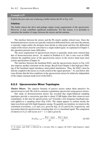
![410 Chap. 6. Mixers
CL
)
(t
xBB
LO
t
)
(t
y
t
Figure 6.83 Sampling mixer for upconversion.
For Y2( f), we must also set k to ±1:
Y2( f)|k 5 ±1 5
1
TLO
[2X( f 2 fLO) 1 X( f 1 fLO)]
1
jω
(1 2 e2jωTLO/2
) . (6.143)
However, the term in the second set of brackets must be evaluated at the upcon-
verted frequency. If ω 5 ωLO 1 ωBB, where ωBB denotes the baseband frequency, then
exp(2jωTLO/2) 5 exp(2jπ) exp(2jωBBTLO/2), which, for ωBB 2fLO, reduces to 2(12
jωBBTLO/2). Similarly, if ω 5 2 ωLO 2 ωBB, then exp(2jωTLO/2) ≈ 2 (1 1 jωBBTLO/2).
Adding Y1( f) and Y2( f) gives
[Y1( f) 1 Y2( f)]k 5 ±1 ≈
ωBB
ωLO 1 ωBB
1
jπ
1
1
2
X( f 2 fLO) 1
2
1
jπ
1
1
2
X ( f 1 fLO) ,
(6.144)
indicating that the upconverted output amplitude is proportional to ωBB/(ωLO 1 ωBB) ≈
ωBB/ωLO. Thus, such a mixer is not suited to upconversion.
In Problem 6.14, we study a return-to-zero mixer for upconversion and show that
its conversion gain is still equal to 2/π (for a single-balanced topology). Similarly,
from Example 6.8, a double-balanced passive mixer exhibits a gain of 2/π. Depicted in
Fig. 6.84(a), such a topology is more relevant to TX design than single-balanced structures
because the baseband waveforms are typically available in differential form. We thus focus
on double-balanced mixers here.
While simple and quite linear, the circuit of Fig. 6.84(a) must deal with a number of
issues. First, the bandwidth at nodes X and Y must accommodate the upconverted signal
frequency so as to avoid additional loss. This bandwidth is determined by the on-resistance
of the switches (Ron), their capacitance contributions to the output nodes, and the input
capacitance of the next stage (Cin). Wider switches increase the bandwidth up to the point
where their capacitances overwhelm Cin, but they also present a greater capacitance at the
LO ports.
It is possible to null the capacitance at nodes X and Y by means of resonance. As
illustrated in Fig. 6.84(b) [15], inductor L1 resonates with the total capacitance at X and Y,
and its value is chosen to yield
ωIF 5
1
L1
2
(CX,Y 1 Cin)
, (6.145)](https://image.slidesharecdn.com/rfmicroelectronicsrazavi-230814101614-71259b59/85/RF-MICROELECTRONICS_Razavi-pdf-435-320.jpg)
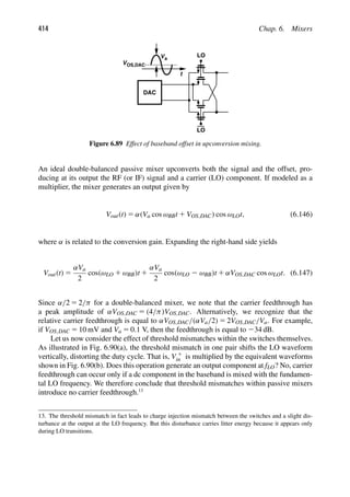
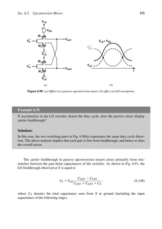
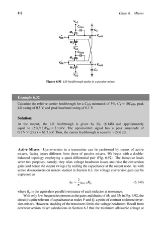
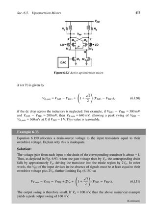
![418 Chap. 6. Mixers
Example 6.33 (Continued)
M 1
LO LO
M M
M M 6
P
3
4
5
Y
X
Va
Va
Figure 6.93 Voltage excursions in an active upconversion mixer.
Unfortunately, the bias conditions of the circuit of Fig. 6.92 heavily depend on the
DAC output common-mode level. Thus, we apply the modification shown in Fig. 6.86,
arriving at the topology in Fig. 6.94(a) (a Gilbert cell). This circuit faces two difficulties.
First, the current source consumes additional voltage headroom. Second, since node A
cannot be held at ac ground by a capacitor at low baseband frequencies, the nonlinearity is
more pronounced. We therefore fold the input path and degenerate the differential pair to
alleviate these issues [Fig. 6.94(b)].
M 1 M
LO LO
VDD
M M
M M 6
DAC
3
4
5
Y
X
VRF
2
LO LO
VDD
M M
M M 6
R
3
4
5
Y
X
Rp
p
VRF
P
Q
RS
I 1
I 3
I 2
I 4
M 1 M 2
Vin2
Vin1
(a) (b)
A
Figure 6.94 (a) Gilbert cell as upconversion mixer, (b) mixer with folded input stage.](https://image.slidesharecdn.com/rfmicroelectronicsrazavi-230814101614-71259b59/85/RF-MICROELECTRONICS_Razavi-pdf-443-320.jpg)
![Sec. 6.5. Upconversion Mixers 423
Example 6.36 (Continued)
V
M 2 M 3
Y
X
VLO
VLO
I SS
out
R Rp
p
VDD
Figure 6.98 Simplified stage for swing calculation.
Solution:
We know that ISS is multiplied by (2/π)Rp as it is upconverted. Thus, the output voltage
swing at ωLO 2ωBB or ωLO 1 ωBB is equal to (2/π)I0Rp. We have assumed that ISS swings
between zero and 2I0, but an input transistor experiencing such a large current variation
may become quite nonlinear.
The above example suggests that I0 must be sufficiently large to yield the required
output swing. That is, with Rp known, I0 can be calculated. A double-balanced version of
the circuit generates twice the output swing, and a quadrature topology (Fig. 6.97) raises
the result by another factor of
√
2, delivering a peak output swing of (4
√
2/π)I0RP. With
I0 ( 5 I3/2 5 I4/2 in Fig. 6.97) known, we select I1 5 I2 5 I3/2 5 I4/2.
How do we select the transistor dimensions? Let us first consider the switching devices,
noting that each switching pair in Fig. 6.97 carries a current of nearly I3 ( 5 I4) at the
extremes of the baseband swings. These transistors must therefore be chosen wide enough
to (1) carry a current of I3 while leaving adequate voltage headroom for I3 and I4, and (2)
switch their tail currents nearly completely with a given LO swing.
Next, the transistors implementing I3 and I4 are sized according to their allowable
voltage headroom. Lastly, the dimensions of the input differential pair and the transistors
realizing I1 and I2 are chosen. With these choices, the input-referred offset [Eq. (6.160)]
must be checked.
Example 6.37
An engineer designs a quadrature upconversion mixer for a given output frequency, a given
output swing, and a given load capacitance, CL. Much to her dismay, the engineer’s man-
ager raises CL to 2CL because the following power amplifier must be redesigned for a
higher output power. If the upconverter output swing must remain the same, how can the
engineer modify her design to drive 2CL?
(Continues)](https://image.slidesharecdn.com/rfmicroelectronicsrazavi-230814101614-71259b59/85/RF-MICROELECTRONICS_Razavi-pdf-448-320.jpg)
![424 Chap. 6. Mixers
Example 6.37 (Continued)
Solution:
Following the calculations outlined previously, we observe that the load inductance and
hence Rp must be halved. Thus, all bias currents and transistor widths must be doubled so
as to maintain the output voltage swing. This in turn translates to a higher load capacitance
seen by the LO. In other words, the larger PA input capacitance “propagates” to the LO
port. Now, the engineer designing the LO is in trouble.
REFERENCES
[1] B. Razavi, “A Millimeter-Wave Circuit Technique,” IEEE J. of Solid-State Circuits, vol. 43,
pp. 2090–2098, Sept. 2008.
[2] P. Eriksson and H. Tenhunen, “The Noise Figure of A Sampling Mixer: Theory and
Measurement,” IEEE Int. Conf. Electronics, Circuits, and Systems, pp. 899–902, Sept. 1999.
[3] S. Zhou and M. C. F. Chang, “A CMOS Passive Mixer with Low Flicker Noise for Low-Power
Direct-Conversion Receivers,” IEEE J. of Solid-State Circuits, vol. 40, pp. 1084, 1093, May
2005.
[4] D. Leenaerts and W. Readman-White, “1/f Noise in Passive CMOS Mixers for Low and Zero
IF Integrated Receivers,” Proc. ESSCIRC, pp. 41–44, Sept. 2001.
[5] A. Mirzaei et al., “Analysis and Optimization of Current-Driven Passive Mixers in Narrow-
band Direct-Conversion Receivers,” IEEE J. of Solid-State Circuits, vol. 44, pp. 2678–2688,
Oct. 2009.
[6] D. Kaczman et al., “A Single-Chip 10-Band WCDMA/HSDPA 4-Band GSM/EDGE SAW-
less CMOS Receiver with DigRF 3G Interface and 190-dBm IIP2,” IEEE J. Solid-State
Circuits, vol. 44, pp. 718–739, March 2009.
[7] H. Darabi and A. A. Abidi, “Noise in RF-CMOS Mixers: A Simple Physical Model,” IEEE
J. of Solid-State Circuits, vol. 35, pp. 15–25, Jan. 2000.
[8] W. H. Sansen and R. G. Meyer, “Distortion in Bipolar Transistor Variable-Gain Amplifiers,”
IEEE Journal of Solid-State Circuits, vol. 8, pp. 275–282, Aug. 1973.
[9] B. Razavi, “A 60-GHz CMOS Receiver Front-End,” IEEE J. of Solid-State Circuits, vol. 41,
pp. 17–22, Jan. 2006.
[10] B. Razavi, “A 900-MHz CMOS Direct-Conversion Receiver,” Dig. of Symposium on VLSI
Circuits, pp. 113–114, June 1997.
[11] M. Brandolini et al., “A 178-dBm IIP2 CMOS Direct Downconversion Mixer for Fully-
Integrated UMTS Receivers,” IEEE J. Solid-State Circuits, vol. 41, pp. 552–559, March
2006.
[12] D. Manstretta, M. Brandolini, and F. Svelto, “Second-Order Intermodulation Mechanisms in
CMOS Downconverters,” IEEE J. Solid-State Circuits, vol. 38, pp. 394–406, March 2003.
[13] H. Darabi and J. Chiu, “A Noise Cancellation Technique in Active RF-CMOS Mixers,” IEEE
J. of Solid-State Circuits, vol. 40, pp. 2628–2632, Dec. 2005.
[14] R. S. Pullela, T. Sowlati, and D. Rozenblit, “Low Flicker Noise Quadrature Mixer Topology,”
ISSCC Dig. Tech. Papers, pp. 76–77, Feb. 2006.
[15] B. Razavi, “CMOS Transceivers for the 60-GHz Band,” IEEE Radio Frequency Integrated
Circuits Symposium, pp. 231–234, June 2006.](https://image.slidesharecdn.com/rfmicroelectronicsrazavi-230814101614-71259b59/85/RF-MICROELECTRONICS_Razavi-pdf-449-320.jpg)
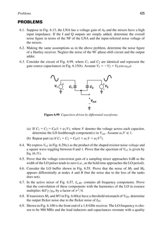
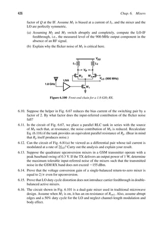
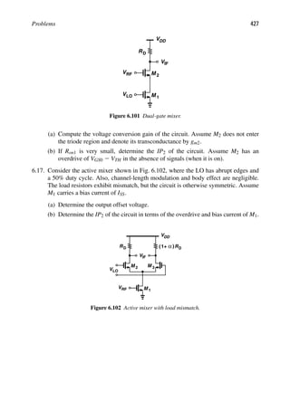

![CHAPTER
7
PASSIVE DEVICES
An important factor in the success of today’s RF integrated circuits has been the ability
to incorporate numerous on-chip passive devices, thus reducing the number of off-chip
components. Of course, some integrated passive devices, especially in CMOS technology,
exhibit a lower quality than their external counterparts. But, as seen throughout this book,
we now routinely use hundreds of such devices in RF transceiver design—an impractical
paradigm if they were placed off-chip.
This chapter deals with the analysis and design of integrated inductors, transformers,
varactors, and constant capacitors. The outline of the chapter is shown below.
Inductors
Basic Structure
Inductance Equations
Parasitic Capacitances
Loss Mechanisms
Inductor Structures
Symmetric Inductors
Stacked Spirals
Effect of Ground Shield
Transformers
Structures
Transformer Modeling
Effect of Coupling
Capacitance
Varactors
PN Junctions
MOS Varactors
Varactor Modeling
Inductor Modeling
7.1 GENERAL CONSIDERATIONS
While analog integrated circuits commonly employ resistors and capacitors, RF design
demands additional passive devices, e.g., inductors, transformers, transmission lines,
and varactors. Why do we insist on integrating these devices on the chip? If the entire
transceiver requires only one or two inductors, why not utilize bond wires or external
components? Let us ponder these questions carefully.
Modern RF design needs many inductors. To understand this point, consider the sim-
ple common-source stage shown in Fig. 7.1(a). This topology suffers from two serious
drawbacks: (a) the bandwidth at node X is limited to 1/[(RD||rO1)CD], and (b) the voltage
headroom trades with the voltage gain, gm1(RD||rO1). CMOS technology scaling tends to
improve the former but at the cost of the latter. For example, in 65-nm technology with a
429](https://image.slidesharecdn.com/rfmicroelectronicsrazavi-230814101614-71259b59/85/RF-MICROELECTRONICS_Razavi-pdf-454-320.jpg)
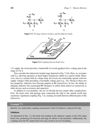
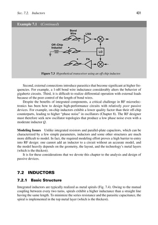
![Sec. 7.2. Inductors 433
The inductance primarily depends on the number of turns and the diameter of each turn,
but the line width and spacing indirectly affect these two parameters.
Example 7.3
The line width of a spiral is doubled to reduce its resistance; Dout, S, and N remain constant.
How does the inductance change?
Solution:
As illustrated in Fig. 7.6, the doubling of the width inevitably decreases the diameter of the
inner turns, thus lowering their inductance, and the larger spacing between the legs reduces
their mutual coupling. We note that further increase in W may also lead to fewer turns,
reducing the inductance.
W
W 2
1
D D
out out
Figure 7.6 Effect of doubling line width of a spiral.
Compared with transistors and resistors, inductors typically have much greater dimen-
sions (“foot prints”), resulting in a large chip area and long interconnects traveling from
one block to another. It is therefore desirable to minimize the outer dimensions of induc-
tors. For a given inductance, this can be accomplished by (a) decreasing W [Fig. 7.7(a)],
or (b) increasing N [Fig. 7.7(b)]. In the former case, the line resistance rises, degrading the
inductor quality. In the latter case, the mutual coupling between the sides of the innermost
turns reduces the inductance because opposite sides carry currents in opposite directions.
As shown in Fig. 7.7(b), the two opposite legs of the innermost turn produce opposing
magnetic fields, partially cancelling each other’s inductance.
Example 7.4
Figure 7.8 plots the magnetic coupling factor between two straight metal lines as a function
of their normalized spacing, S/W. Obtained from electromagnetic field simulations, the
plots correspond to two cases: each line is 20 μm or 100 μm long. (The line width is 4 μm.)
What inner diameter do these plots prescribe for spiral inductors?
(Continues)](https://image.slidesharecdn.com/rfmicroelectronicsrazavi-230814101614-71259b59/85/RF-MICROELECTRONICS_Razavi-pdf-458-320.jpg)
![436 Chap. 7. Passive Devices
7.2.3 Inductance Equations
With numerous inductors used in a typical transceiver, it is desirable to have closed-form
equations that provide the inductance value in terms of the spiral’s geometric properties.
Indeed, various inductance expressions have been reported in the literature [1–3], some
based on curve fitting and some based on physical properties of inductors. For example,
an empirical formula that has less than 10% error for inductors in the range of 5 to 50 nH
is given in [1] and can be reduced to the following form for a square spiral:
L ≈ 1.3 3 1027 A
5/3
m
A
1/6
tot W1.75(W 1 S)0.25
, (7.2)
where Am is the metal area (the shaded area in Fig. 7.5) and Atot is the total inductor area
(≈ D2
out in Fig. 7.5). All units are metric.
Example 7.5
Calculate the inductor metal area in terms of the other geometric properties.
Solution:
Consider the structure shown in Fig. 7.10. We say this spiral has three turns because each
of the four sides contains three complete legs. To determine the metal area, we compute the
total length, ltot, of the wire and multiply it by W. The length from A to B is equal to Dout,
from B to C, equal to Dout 2 W, etc. That is,
lAB 5 Dout (7.3)
lBC 5 lCD 5 Dout 2 W (7.4)
lDE 5 lEF 5 Dout 2 (2W 1 S) (7.5)
lFG 5 lGH 5 Dout 2 (3W 1 2S) (7.6)
lHI 5 lIJ 5 Dout 2 (4W 1 3S) (7.7)
lJK 5 lKL 5 Dout 2 (5W 1 4S) (7.8)
lLM 5 Dout 2 (6W 1 5S). (7.9)
Adding these lengths and generalizing the result for N turns, we have
ltot 5 4NDout 2 2W[1 1 2 1 · · · 1 (2N 2 1)] 2 2NW
2 2S[1 1 2 1 · · · 1 (2N 2 2)] 2 (2N 2 1)S (7.10)
5 4NDout 2 4N2
W 2 (2N 2 1)2
S. (7.11)
Since ltot S, we can add one S to the right-hand side so as to simplify the expression:
ltot ≈ 4N[Dout 2 W 2 (N 2 1)(W 1 S)]. (7.12)](https://image.slidesharecdn.com/rfmicroelectronicsrazavi-230814101614-71259b59/85/RF-MICROELECTRONICS_Razavi-pdf-461-320.jpg)
![Sec. 7.2. Inductors 437
Example 7.5 (Continued)
The metal area is thus given by
Am 5 W[4NDout 2 4N2
W 2 (2N 2 1)2
S] (7.13)
≈ 4NW[Dout 2 W 2 (N 2 1)(W 1 S)]. (7.14)
This equation is also used for calculating the area capacitance of the spiral.
A
B
C D
E
F
G
H
I
J
K
L
M
Dout
W
Figure 7.10 Spiral inductor for calculation of line length.
An interesting property of inductors is that, for a given wire length, width, and spacing,
their inductance is a weak function of the number of turns. This can be seen by finding Dout
from (7.12), noting that Atot ≈ D2
out, and manipulating (7.2) as follows:
L ≈ 1.3 3 1027 l
5/3
tot
ltot
4N
1 W 1 (N 2 1)(W 1 S)
1/3
W0.083(W 1 S)0.25
. (7.15)
We observe that N appears only within the square brackets in the denominator, in two terms
varying in opposite directions, with the result raised to the power of 1/3. For example,
if ltot 5 2000 μm, W 5 4 μm, and S 5 0.5 μm, then as N varies from 2 to 3 to 4 to 5,
then inductance rises from 3.96 nH to 4.47 nH to 4.83 nH to 4.96 nH, respectively. In other
words, a given length of wire yields roughly a constant inductance regardless of how it is
“wound.”3
The key point here is that, since this length has a given series resistance (at low
frequencies), the choice of N only mildly affects the Q (but can save area).
Figure 7.11 plots the inductance predicted by the simulator ASITIC (described below)
as N varies from 2 to 6 and the total wire length remains at 2000 μm.4
We observe that L
becomes relatively constant for N 3. Also, the values produced by ASITIC are lower
than those given by Eq. (7.15).
3. But the number of turns must be at least 2 to create mutual coupling.
4. The outer dimension varies from 260 μm to 110 μm in this experiment.](https://image.slidesharecdn.com/rfmicroelectronicsrazavi-230814101614-71259b59/85/RF-MICROELECTRONICS_Razavi-pdf-462-320.jpg)
![438 Chap. 7. Passive Devices
2 3 4 5 6 N
Dout
260 180 142 120 110 (μm)
3.0
3.5
4.0
4.5
5.0
L
(nH)
Figure 7.11 Inductance as a function of the number of turns for a given line length.
A number of other expressions have been proposed for the inductance of spirals. For
example,
L 5
μ0N2Davgα1
2
ln
α2
ρ
1 α3ρ 1 α4ρ2
, (7.16)
where Davg 5 (Dout 1 Din)/2 in Fig. 7.5 and ρ is the “fill factor” and equal to (Dout 2
Din)/(Dout 1 Din) [3]. The α coefficients are chosen as follows [3]:
α1 5 1.27, α2 5 2.07, α3 5 0.18, α4 5 0.13 for square shape (7.17)
α1 5 1.07, α2 5 2.29, α3 5 0, α4 5 0.19 for octagonal shape. (7.18)
Another empirical expression is given by [3]
L 5 1.62 3 1023
D21.21
out W20.147
D2.4
avgN1.78
S20.03
for square shape (7.19)
L 5 1.33 3 1023
D21.21
out W20.163
D2.43
avg N1.75
S20.049
for octagonal shape. (7.20)
Accuracy Considerations The above inductance equations yield different levels of accu-
racy for different geometries. For example, the measurements on tens of inductors in [3]
reveal that Eqs. (7.19) and (7.20) incur an error of about 8% for 20% of the inductors
and an error of about 4% for 50% of the inductors. We must then ask: how much error
is tolerable in inductance calculations? As observed throughout this book and exempli-
fied by Fig. 7.1(b), inductors must typically resonate with their surrounding capacitances
at the desired frequency. Since a small error of L/L shifts the resonance frequency, ω0,
by approximately L/(2L) (why?), we must determine the tolerable error in ω0.
The resonance frequency error becomes critical in amplifiers and oscillators, but much
more so in the latter. This is because, as seen abundantly in Chapter 8, the design of LC
oscillators faces tight trade-offs between the “tuning range” and other parameters. Since
the tuning range must encompass the error in ω0, a large error dictates a wider tuning
range, thereby degrading other aspects of the oscillator’s performance. In practice, the tun-
ing range of high-performance LC oscillators rarely exceeds ±10%, requiring that both
capacitance and inductance errors be only a small fraction of this value, e.g., a few per-
cent. Thus, the foregoing inductance expressions may not provide sufficient accuracy for
oscillator design.](https://image.slidesharecdn.com/rfmicroelectronicsrazavi-230814101614-71259b59/85/RF-MICROELECTRONICS_Razavi-pdf-463-320.jpg)
![Sec. 7.2. Inductors 439
Another issue with respect to inductance equations stems from the geometry limitations
that they impose. Among the topologies shown in Fig. 7.9, only a few lend themselves
to the above formulations. For example, the subtle differences between the structures in
Figs. 7.9(b) and (c) or the parallel combination of the spirals in Fig. 7.9(f) may yield several
percent of error in inductance predictions.
Another difficulty is that the inductance value also depends on the frequency of
operation—albeit weakly—while most equations reported in the literature predict the
low-frequency value. We elaborate on this dependence in Section 7.2.6.
Field Simulations With the foregoing sources of error in mind, how do we compute
the inductance in practice? We may begin with the above approximate equations for stan-
dard structures, but must eventually resort to electromagnetic field simulations for standard
or nonstandard geometries. A field simulator employs finite-element analysis to solve the
steady-state field equations and compute the electrical properties of the structure at a given
frequency.
A public-domain field simulator developed for analysis of inductors and transformers
is called “Analysis and Simulation of Spiral Inductors and Transformers” (ASITIC) [4].
The tool can analyze a given structure and report its equivalent circuit components. While
simple and efficient, ASITIC also appears to exhibit inaccuracies similar to those of the
above equations [3, 5].5
Following rough estimates provided by formulas and/or ASITIC, we must analyze the
structure in a more versatile field simulator. Examples include Agilent’s “ADS,” Sonnet
Software’s “Sonnet,” and Ansoft’s “HFSS.” Interestingly, these tools yield slightly different
values, partly due to the types of approximations that they make. For example, some do
not accurately account for the thickness of the metal layers. Owing to these discrepancies,
RF circuits sometimes do not exactly hit the targeted frequencies after the first fabrication,
requiring slight adjustments and “silicon iterations.” As a remedy, we can limit our usage
to a library of inductors that have been measured and modeled carefully but at the cost of
flexibility in design and layout.
7.2.4 Parasitic Capacitances
As a planar structure built upon a substrate, spiral inductors suffer from parasitic capac-
itances. We identify two types. (1) The metal line forming the inductor exhibits parallel-
plate and fringe capacitances to the substrate [Fig. 7.12(a)]. If a wider line is chosen to
reduce its resistance, then the parallel-plate component increases. (2) The adjacent turns
also bear a fringe capacitance, which equivalently appears in parallel with each segment
[Fig. 7.12(b)].
Let us first examine the effect of the capacitance to the substrate. Since in most cir-
cuits, one terminal of the inductor is at ac ground, we construct the uniformly-distributed
equivalent circuit shown in Fig. 7.13, where each segment has an inductance of Lu. Our
objective is to obtain a lumped model for this network. To simplify the analysis, we make
two assumptions: (1) each two inductor segments have a mutual coupling of M, and (2)
5. In fact, Eqs. (7.19) and (7.20) have been developed based on ASITIC simulations.](https://image.slidesharecdn.com/rfmicroelectronicsrazavi-230814101614-71259b59/85/RF-MICROELECTRONICS_Razavi-pdf-464-320.jpg)
![440 Chap. 7. Passive Devices
(a) (b)
Fringe
Capacitance
Capacitance
Parallel−Plate
Figure 7.12 (a) Bottom-plate and (b) interwinding capacitances of an inductor and their models.
V1
1 2 3
L1 L2
Cu Cu
L
Cu Cu
n
n−1 Ln
I n
n +1
Vn
Ln+1 L
Cu
L
K−1 K
Figure 7.13 Model of an inductor’s distributed capacitance to ground.
the coupling is strong enough that M can be assumed approximately equal to Lu. While not
quite valid, these assumptions lead to a relatively accurate result.
The voltage across each inductor segment arises from the current flowing through that
segment and the currents flowing through the other segments. That is,
Vn 5 jωLnIn 1
n21
m51
jωImM 1
K
m5n11
jωImM. (7.21)
If M ≈ Lu, then
Vn 5 jω
K
m51
ImLm. (7.22)
Since this summation is independent of n, we note that all inductor segments sustain equal
voltages [6]. The voltage at node n is therefore given by (n/K)V1, yielding an electric
energy stored in the corresponding node capacitance equal to
Eu 5
1
2
Cu
n
K
2
V2
1 . (7.23)
Summing the energies stored on all of the unit capacitances, we have
Etot 5
1
2
Cu
K
n51
n
K
2
V2
1 (7.24)
5
1
2
Cu
(K 1 1)(2K 1 1)
6K
V2
1 . (7.25)](https://image.slidesharecdn.com/rfmicroelectronicsrazavi-230814101614-71259b59/85/RF-MICROELECTRONICS_Razavi-pdf-465-320.jpg)
![Sec. 7.2. Inductors 441
If K → ∞ and Cu → 0 such that KCu is equal to the total wire capacitance, Ctot, then [6]
Etot 5
1
2
Ctot
3
V2
1 , (7.26)
revealing that the equivalent lumped capacitance of the spiral is given by Ctot/3 (if one end
is grounded).
Let us now study the turn-to-turn (interwinding) capacitance. Using the model shown
in Fig. 7.14, where C1 5 C2 5 · · · 5 CK 5 CF, we recognize that Eq. (7.22) still applies
for it is independent of capacitances. Thus, each capacitor sustains a voltage equal to V1/K,
storing an electric energy of
Eu 5
1
2
CF
1
K
V1
2
. (7.27)
The total stored energy is given by
Etot 5 KEu (7.28)
5
1
2K
CFV2
1 . (7.29)
Interestingly, Etot falls to zero as K → ∞ and CF → 0. This is because, for a large number
of turns, the potential difference between adjacent turns becomes very small, yielding a
small electric energy stored on the CF’s.
V1
2 3
L1 L2 L n
n−1 Ln
I n
n +1
V
Ln+1 L L
K−1 K
n
C1 C2 Cn−1 C C
n n+1 C CK
K−1
1
Figure 7.14 Model of an inductor’s turn-to-turn capacitances.
In practice, we can utilize Eq. (7.29) to estimate the equivalent lumped capacitance for
a finite number of turns. The following example illustrates this point.
Example 7.6
Estimate the equivalent turn-to-turn capacitance of the three-turn spiral shown in
Fig. 7.15(a).
Solution:
An accurate calculation would “unwind” the structure, modeling each leg of each turn by
an inductance and placing the capacitances between adjacent legs [Fig. 7.15(b)]. Unfortu-
nately, owing to the unequal lengths of the legs, this model entails unequal inductances and
capacitances, making the analysis difficult. To arrive at a uniformly-distributed model, we
select the value of Cj equal to the average of C1, . . . , C8, and Lj equal to the total inductance
(Continues)](https://image.slidesharecdn.com/rfmicroelectronicsrazavi-230814101614-71259b59/85/RF-MICROELECTRONICS_Razavi-pdf-466-320.jpg)
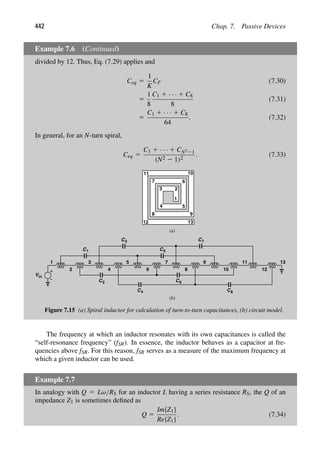
![Sec. 7.2. Inductors 443
Example 7.7 (Continued)
Compute this Q for the parallel inductor model shown in Fig. 7.16(a).
Rp
L1
C1
Z 1
f
fSR
Z
Re{ }
Z }
Im{
Q =
(a) (b)
in1
in1
Figure 7.16 (a) Simple tank and (b) behavior of one definition of Q.
Solution:
We have
Z1(s) 5
RpL1s
RpL1C1s2 1 L1s 1 Rp
. (7.35)
At s 5 jω,
Z1(jω) 5
[Rp(1 2 L1C1ω2) 2 jL1ω]jRpL1ω
R2
p(1 2 L1C1ω2)2 1 L2
1ω2
. (7.36)
It follows that
Q 5
Rp(1 2 L1C1ω2)
L1ω
(7.37)
5
Rp
L1ω
1 2
ω2
ω2
SR
, (7.38)
where ωSR 5 2πfSR 5 1/
√
L1C1. At frequencies well below ωSR, we have Q ≈ Rp/(L1ω),
which agrees with our definition in Chapter 2. On the other hand, as the frequency
approaches fSR, Q falls to zero [Fig. 7.16(b)]—as if the tank were useless! This defini-
tion implies that a general impedance (including additional capacitances due to transistors,
etc.) exhibits a Q of zero at resonance. Of course, the tank of Fig. 7.16(a) simply reduces to
resistor Rp at fSR, providing a Q of Rp/(L1ωSR) rather than zero. Owing to its meaningless
behavior around resonance, the Q definition given by Eq. (7.34) proves irrelevant to circuit
design. We return to this point in Section 7.2.6.
Example 7.8
In analogy with L1 5 impedance/ω 5 (L1ω)/ω, the equivalent inductance of a structure is
sometimes defined as Im{Z1(jω)}/ω. Study this inductance definition for the parallel tank
of Fig. 7.16(a) as a function of frequency.
(Continues)](https://image.slidesharecdn.com/rfmicroelectronicsrazavi-230814101614-71259b59/85/RF-MICROELECTRONICS_Razavi-pdf-468-320.jpg)
![444 Chap. 7. Passive Devices
Example 7.8 (Continued)
Solution:
From Eq. (7.36), we have
Im{Z1(jω)}
ω
5
R2
pL1(1 2 L1C1ω2)
R2
p(1 2 L1C1ω2)2 1 L2
1ω2
. (7.39)
This expression simplifies to L1 at frequencies well below fSR but falls to zero at reso-
nance! The actual inductance, however, varies only slightly with frequency. This definition
of inductance is therefore meaningless. Nonetheless, its value at low frequencies proves
helpful in estimating the inductance.
7.2.5 Loss Mechanisms
The quality factor, Q, of inductors plays a critical role in various RF circuits. For example,
the phase noise of oscillators is proportional to 1/Q2 (Chapter 8), and the voltage gain of
“tuned amplifiers” [e.g., the CS stage in Fig. 7.1(b)] is proportional to Q. In typical CMOS
technologies and for frequencies up to 5 GHz, a Q of 5 is considered moderate and a Q
of 10, relatively high.
We define the Q carefully in Section 7.2.6, but for now we consider Q as a measure
of how much energy is lost in an inductor when it carries a sinusoidal current. Since only
resistive components dissipate energy, the loss mechanisms of inductors relate to various
resistances within or around the structure that carry current when the inductor does.
In this section, we study these loss mechanisms. As we will see, it is difficult to
formulate the losses analytically; we must therefore resort to simulations and even mea-
surements to construct accurate inductor models. Nonetheless, our understanding of the
loss mechanisms helps us develop guidelines for inductor modeling and design.
Metal Resistance Suppose the metal line forming an inductor exhibits a series resistance,
RS (Fig. 7.17). The Q may be defined as the ratio of the desirable impedance, L1ω0, and the
undesirable impedance, RS:
Q 5
L1ω0
RS
. (7.40)
For example, a 5-nH inductor operating at 5 GHz with an RS of 15.7 has a Q of 10.
Figure 7.17 Metal resistance in a spiral inductor.](https://image.slidesharecdn.com/rfmicroelectronicsrazavi-230814101614-71259b59/85/RF-MICROELECTRONICS_Razavi-pdf-469-320.jpg)
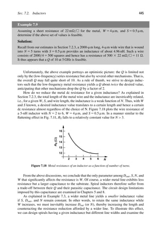
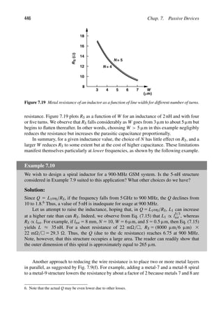
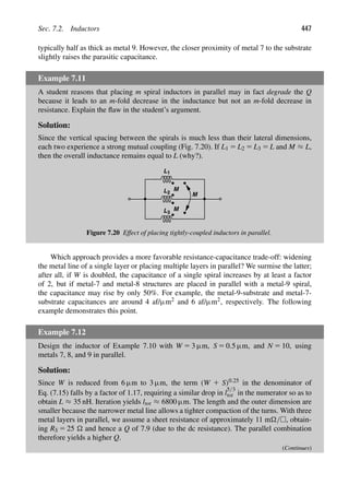
![448 Chap. 7. Passive Devices
Example 7.12 (Continued)
It is instructive to compare the capacitances of the metal-9 spiral in Exam-
ple 7.10 and the above multi-layer structure. For the former, the total metal area is
ltot · W 5 48, 000 μm2, yielding a capacitance of (4 af/μm2) 3 48, 000 μm2 5 192 fF.7
For the latter, the area is equal to 20,400 μm2 and the capacitance is 122.4 fF.
Skin Effect At high frequencies, the current through a conductor prefers to flow at
the surface. If the overall current is viewed as many parallel current components, these
components tend to repel each other, migrating away so as to create maximum distance
between them. This trend is illustrated in Fig. 7.21. Flowing through a smaller cross section
area, the high-frequency current thus faces a greater resistance. The actual distribution
of the current follows an exponential decay from the surface of the conductor inward,
J(s) 5 J0 exp(2x/δ), where J0 denotes the current density (in A/m2
) at the surface, and
δ is the “skin depth.” The value of δ is given by
δ 5
1
√
πfμσ
, (7.41)
where f denotes the frequency, μ the permeability, and σ the conductivity. For example,
δ ≈ 1.4 μm at 10 GHz for aluminum. The extra resistance of a conductor due to the skin
effect is equal to
Rskin 5
1
σδ
. (7.42)
Parallel spirals can reduce this resistance if the skin depth exceeds the sum of the metal
wire thicknesses.
(a) (b)
Figure 7.21 Current distribution in a conductor at (a) low and (b) high frequencies.
In spiral inductors, the proximity of adjacent turns results in a complex current distri-
bution. As illustrated in Fig. 7.22(a), the current may concentrate near the edge of the wire.
To understand this “current crowding” effect, consider the more detailed diagram shown
in Fig. 7.22(b), where each turn carries a current of I(t) [7, 8]. The current in one turn
creates a time-varying magnetic field, B, that penetrates the other turns, generating loops of
current.8
Called “eddy currents,” these components add to I(t) at one edge of the wire and
7. The equivalent (lumped) capacitance of the inductor is less than this value (Section 7.2.4).
8. Faraday’s law states that the voltage induced in a conducting circuit is proportional to the time derivative of
the magnetic field.](https://image.slidesharecdn.com/rfmicroelectronicsrazavi-230814101614-71259b59/85/RF-MICROELECTRONICS_Razavi-pdf-473-320.jpg)
![Sec. 7.2. Inductors 449
B
I )
(t
Magnetic Field
Produced by I
Produced by
Eddy Current
B
I )
(t
(a) (b)
Figure 7.22 (a) Current distribution in adjacent turns, (b) detailed view of (a).
subtract from I(t) at the other edge. Since the induced voltage increases with frequency,
the eddy currents and hence the nonuniform distribution become more prominent at higher
frequencies.
Based on these observations, [7, 8] derive the following expression for the resistance
of a spiral inductor:
Reff ≈ R0
1 1
1
10
f
fcrit
2
, (7.43)
where R0 is the dc resistance and the frequency fcrit denotes the onset of current crowding
and is given by
fcrit ≈
3.1
2πμ
W 1 S
W2
R. (7.44)
In this equation, R represents the dc sheet resistance of the metal.
Example 7.13
Calculate the series resistance of the 30-nH inductors studied in Examples 7.9 and 7.12 at
900 MHz. Assume μ 5 4π 3 1027 H/m.
Solution:
For the single-layer spiral, R 5 22 m/, W 5 6 μm, S 5 0.5 μm, and hence fcrit 5
1.56 GHz. Thus, Reff 5 1.03R0 5 30.3 . For the multilayer spiral, R 5 11 m/,
W 5 3 μm, S 5 0.5 μm, and hence fcrit 5 1.68 GHz. We therefore have Reff 5
1.03R0 5 26 .
Current crowding also alters the inductance and capacitance of spiral geometries. Since
the current is pushed to the edge of the wire, the equivalent diameter of each turn changes
slightly, yielding an inductance different from the low-frequency value. Similarly, as illus-
trated in Fig. 7.23(a), if a conductor carries currents only near the edges, then its middle
section can be “carved out” without altering the currents and voltages, suggesting that the
capacitance of this section, Cm, is immaterial. From another perspective, Cm manifests
itself only if it carries displacement current, which is not possible if the middle section has
no current. Based on this observation, [7, 8] approximate the total capacitance, Ctot, to vary](https://image.slidesharecdn.com/rfmicroelectronicsrazavi-230814101614-71259b59/85/RF-MICROELECTRONICS_Razavi-pdf-474-320.jpg)
![450 Chap. 7. Passive Devices
Cm
No Current Flow
Figure 7.23 Reduction of capacitance to the substrate as a result of current crowding.
inversely proportional to the wire resistance:
Ctot ≈
R0
Reff
C0, (7.45)
where C0 denotes the low-frequency capacitance.
Capacitive Coupling to Substrate We have seen in our studies that spirals exhibit capac-
itance to the substrate. As the voltage at each point on the spiral rises and falls with
time, it creates a displacement current that flows through this capacitance and the substrate
(Fig. 7.24). Since the substrate resistivity is neither zero nor infinity, this flow of current
translates to loss in each cycle of the operation, lowering the Q.
Figure 7.24 Substrate loss due to capacitive coupling.
Example 7.14
Use a distributed model of a spiral inductor to estimate the power lost in the substrate.
Solution:
We model the structure by K sections as shown in Fig. 7.25(a). Here, each section consists
of an inductance equal to Ltot/K, a capacitance equal to Ctot/K, and a substrate resistance
equal to KRsub. (The other loss mechanisms are ignored here.) The factor of K in KRsub
is justified as follows: as we increase K for a given inductor geometry (i.e., as the dis-
tributed model approaches the actual structure), each section represents a smaller segment
of the spiral and hence a smaller cross section area looking into the substrate [Fig. 7.25(b)].
Consequently, the equivalent resistance increases proportionally.](https://image.slidesharecdn.com/rfmicroelectronicsrazavi-230814101614-71259b59/85/RF-MICROELECTRONICS_Razavi-pdf-475-320.jpg)
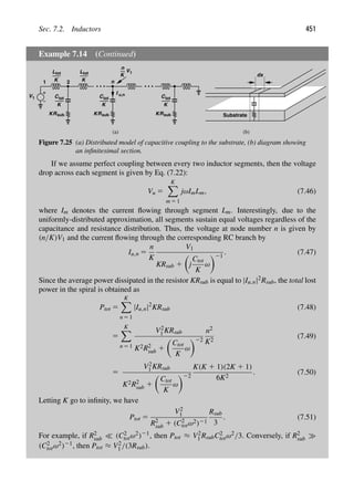
![452 Chap. 7. Passive Devices
The foregoing example provides insight into the power loss due to capacitive cou-
pling to the substrate. The distributed model of the substrate, however, is not accurate. As
depicted in Fig. 7.26(a), since the connection of the substrate to ground is physically far,
some of the displacement current flows laterally in the substrate. Lateral substrate currents
are more pronounced between adjacent turns [Fig. 7.26(b)] because their voltage differ-
ence, V1 2 V2, is larger than the incremental drops in Fig. 7.26(a), Vn11 2 Vn. The key
point here is that the inductor-substrate interaction can be quantified accurately only if a
three-dimensional model is used, but a rare case in practice.
Substrate
Vn Vn+1 Vn+2
(a) (b)
V1 V2
Figure 7.26 Lateral current flow in the substrate (a) under a branch, and (b) from one branch to
another.
Magnetic Coupling to the Substrate The magnetic coupling from an inductor to the
substrate can be understood with the aid of basic electromagnetic laws: (1) Ampere’s law
states that a current flowing through a conductor generates a magnetic field around the con-
ductor; (2) Faraday’s law states that a time-varying magnetic field induces a voltage, and
hence a current if the voltage appears across a conducting material; (3) Lenz’s law states
that the current induced by a magnetic field generates another magnetic field opposing the
first field.
Ampere’s and Faraday’s laws readily reveal that, as the current through an inductor
varies with time, it creates an eddy current in the substrate (Fig. 7.27). Lenz’s law implies
that the current flows in the opposite direction. Of course, if the substrate resistance were
infinity, no current would flow and no loss would occur.
The induction of eddy currents in the substrate can also be viewed as transformer cou-
pling. As illustrated in Fig. 7.28(a), the inductor and the substrate act as the primary and
Magnetic
Field
Eddy
Current
Figure 7.27 Magnetic coupling to the substrate.](https://image.slidesharecdn.com/rfmicroelectronicsrazavi-230814101614-71259b59/85/RF-MICROELECTRONICS_Razavi-pdf-477-320.jpg)
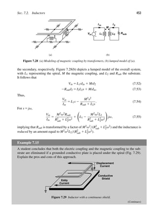
![454 Chap. 7. Passive Devices
Example 7.15 (Continued)
Solution:
This method indeed reduces the path resistance seen by both displacement and eddy cur-
rents. Unfortunately, however, Eq. (7.55) reveals that the equivalent inductance also falls
with Rsub. For Rsub 5 0,
Leq 5 L1 2
M2
L2
. (7.56)
Since the vertical spacing between the spiral and the conductive plate (≈ 5 μm) is much
smaller than their lateral dimensions, we have M ≈ L2 ≈ L1, obtaining a very small value
for Leq. In other words, even though the substrate losses are reduced, the drastic fall in the
equivalent inductance still yields a low Q because of the spiral’s resistance.
It is instructive to consider a few special cases of Eq. (7.54). If L1 5 L2 5 M, then
Vin
Iin
5 L1s||Rsub, (7.57)
indicating that Rsub simply appears in parallel with L1, lowering the Q.
Example 7.16
Sketch the Q of a given inductor as a function of frequency.
Solution:
At low frequencies, the Q is given by the dc resistance of the spiral, RS. As the frequency
increases, Q 5 L1ω/RS rises linearly up to a point where skin effect becomes significant
[Fig. 7.30(a)]. The Q then increases in proportion to
√
f. At higher frequencies, L1ω RS,
and Eq. (7.57) reveals that Rsub shunts the inductor, limiting the Q to
Q ≈
Rsub
L1ω
, (7.58)
which falls with frequency. Figure 7.30(b) sketches the behavior.
L1
RS
L1
RS
Rskin
L1
RS
Rskin
Rsub
Low
Frequencies Frequencies
High
Frequencies
Very High
ω
Q
L1ω
RS
L1ω
RS+Rskin
L1ω
Rsub
(a) (b)
Figure 7.30 (a) Inductor model reflecting loss at different frequencies, (b) corresponding Q
behavior.](https://image.slidesharecdn.com/rfmicroelectronicsrazavi-230814101614-71259b59/85/RF-MICROELECTRONICS_Razavi-pdf-479-320.jpg)
![Sec. 7.2. Inductors 455
As another special case, suppose Rsub |L2s|. We can then factor L2s out in Eq. (7.54)
and approximate the result as
Vin
Iin
5
L1 2
M2
L2
s 1
M2
L2
2
Rsub. (7.59)
Thus, as predicted in Example 7.15, the inductance is reduced by an amount equal to
M2/L2. Moreover, the substrate resistance is transformed by a factor of M2/L2
2 and appears
in series with the net inductance.
7.2.6 Inductor Modeling
Our study of various effects in spiral inductors has prepared us for developing a circuit
model that can be used in simulations. Ideally, we wish to obtain a model that retains our
physical insights and is both simple and accurate. In practice, some compromise must be
made.
It is important to note that (1) both the spiral and the substrate act as three-dimensional
distributed structures and can only be approximated by a two-dimensional lumped model;
(2) due to skin effect, current-crowding effects, and eddy currents, some of the inductor
parameters vary with frequency, making it difficult to fit the model in a broad bandwidth.
Example 7.17
If RF design mostly deals with narrowband systems, why is a broadband model necessary?
Solution:
From a practical point of view, it is desirable to develop a broadband model for a given
inductor structure so that it can be used by multiple designers and at different frequencies
without repeating the modeling effort each time. Moreover, RF systems such as ultra-
wideband (UWB) and cognitive radios do operate across a wide bandwidth, requiring
broadband models.
Let us begin with a model representing metal losses. As shown in Fig. 7.31(a), a series
resistance can embody both low-frequency and skin resistance. With a constant RS, the
model is valid for a limited frequency range. As explained in Chapter 2, the loss can alter-
natively be modeled by a parallel resistance [Fig. 7.31(b)] but still for a narrow range if Rp
is constant.
L1
RS
L1 Rp
(a) (b)
Figure 7.31 Modeling loss by (a) series or (b) parallel resistors.](https://image.slidesharecdn.com/rfmicroelectronicsrazavi-230814101614-71259b59/85/RF-MICROELECTRONICS_Razavi-pdf-480-320.jpg)
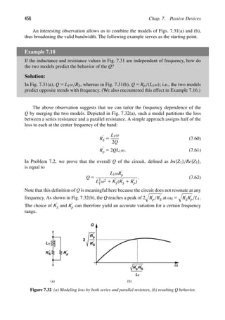
![Sec. 7.2. Inductors 457
1 n
2
R
R L
1
2 2
R L
3 3
(a) (b)
R S1 L1
R S2
L2
(c)
Figure 7.33 (a) Broadband model of inductor, (b) view of a conductor as concentric cylinders,
(c) broadband skin effect model.
A more general model of skin effect has been proposed by [9] and is illustrated in
Fig. 7.33. Suppose a model must be valid only at dc and a high frequency. Then, as shown
in Fig. 7.33(a), we select a series resistance, RS1, equal to that due to skin effect and shunt
the combination of RS1 and L1 with a large inductor, L2. We then add RS2 in series to model
the low-frequency resistance of the wire. At high frequencies, L2 is open and RS1 1 RS2
embodies the overall loss; at low frequencies, the network reduces to RS2.
The above principle can be extended to broadband modeling of skin effect. Depicted in
Fig. 7.33(b) for a cylindrical wire, the approach in [9] views the line as a set of concentric
cylinders, each having some low-frequency resistance and inductance, arriving at the circuit
in Fig. 7.33(c) for one section of the distributed model. Here, the branch consisting of Rj
and Lj represents the impedance of cylinder number j. At low frequencies, the current is
uniformly distributed through the conductor and the model reduces to R1||R2|| · · · ||Rn [9].
As the frequency increases, the current moves away from the inner cylinders, as modeled
by the rising impedance of the inductors in each branch. In [9], a constant ratio Rj/Rj11 is
maintained to simplify the model. We return to the use of this model for inductors later in
this section.
We now add the effect of capacitive coupling to the substrate. Figure 7.34(a) shows
a one-dimensional uniformly-distributed model where the total inductance and series
resistance are decomposed into n equal segments, i.e., L1 1 L2 1 · · · 1 Ln 5 Ltot and
RS1 1 RS2 1 · · · 1 RSn 5 RS,tot.9
The nodes in the substrate are connected to one another
by Rsub1, . . . , Rsub,n21 and to ground by RG1, . . . , RGn. The total capacitance between the
spiral and the substrate is decomposed into Csub1, . . . , Csubn.
Continuing our model development, we include the magnetic coupling to the substrate.
As depicted in Fig. 7.34(b), each inductor segment is coupled to the substrate through a
transformer. Proper choice of the mutual coupling and Rsubm allows accurate representation
of this type of loss. In this model, the capacitance between the substrate nodes is also
included.
While capturing the physical properties of inductors, the model shown in Fig. 7.34(b)
proves too complex for practical use. The principal issue is that the numerous parameters
make it difficult to fit the model to measured data. We must therefore seek more compact
models that more easily lend themselves to parameter extraction and fitting. In the first
9. A more accurate model would include mutual coupling such that Ltot 5 L1 1 · · · 1 Ln 1 nM.](https://image.slidesharecdn.com/rfmicroelectronicsrazavi-230814101614-71259b59/85/RF-MICROELECTRONICS_Razavi-pdf-482-320.jpg)
![458 Chap. 7. Passive Devices
R
L1 R
L
Csub1
RG1
Rsub1
S1 2 S2
C
R
sub2
G2
R
L
C
R
n Sn
subn
Gn
Rsub,n−1
R
L1 R
L
Csub1
RG1
Rsub1
S1 2 S2
C
R
sub2
G2
R
L
C
R
n Sn
subn
Gn
Rsub,n−1
Rsubm Rsubm Rsubm
(a)
(b)
Figure 7.34 Distributed inductor model with (a) capacitive and (b) magnetic coupling to substrate.
R
C C
S
1 2
(a) (b)
′
L1
CF
R R
R′
p
RS
′
L1
CF
1 2
C1
C3
C2
C4
Figure 7.35 (a) Compact inductor model, (b) alternative topology.
step, we turn to lumped models. As a simple example, we return to the parallel-series
combination of Fig. 7.32(a) and add capacitances to the substrate [Fig. 7.35(a)]. We surmise
that R9
S and R9
p can represent all of the losses even though they do not physically reflect the
substrate loss. We also recall from Section 7.2.4 that an equivalent lumped capacitance, CF,
appears between the two terminals. With constant element values, this model is accurate
for a bandwidth of about ±20% around the center frequency.
An interesting dilemma arises in the above lumped model. We may choose C1 and C2
to be equal to half of the total capacitance to the substrate, but our analysis in Section 7.2.4
suggests that, if one terminal is grounded, the equivalent capacitance is one-third of the
total amount. This is a shortcoming of the lumped model.](https://image.slidesharecdn.com/rfmicroelectronicsrazavi-230814101614-71259b59/85/RF-MICROELECTRONICS_Razavi-pdf-483-320.jpg)
![Sec. 7.2. Inductors 459
Another model that has proved relatively accurate is shown in Fig. 7.35(b). Here,
R1 and R2 play a similar role to that of Rp in Fig. 7.35(a). Note that neither model explicitly
includes the magnetic coupling to the substrate. The assumption is that the three resistances
suffice to represent all of the losses across a reasonable bandwidth (e.g., ±20% around the
frequency at which the component values are calculated). A more broadband model is
described in [10].
Definitions of Q In this book, we have encountered several definitions of the Q of an
inductor:
Q1 5
Lω
RS
(7.63)
Q2 5
Rp
Lω
(7.64)
Q3 5
Im{Z}
Re{Z}
. (7.65)
In basic physics, the Q of a lossy oscillatory system is defined as
Q4 5 2π
Energy Stored
Energy Dissipated per Cycle
. (7.66)
Additionally, for a second-order tank, the Q can be defined in terms of the resonance
frequency, ω0, and the 23-dB bandwidth, ωBW, as
Q5 5
ω0
ωBW
. (7.67)
To make matters more complicated, we can also define the Q of an open-loop system at a
frequency ω0 as
Q6 5
ω0
2
dφ
dω
, (7.68)
where φ denotes the phase of the system’s transfer function (Chapter 8).
Which one of the above definitions is relevant to RF design? We recall from Chapter 2
that Q1 and Q2 model the loss by a single resistance and are equivalent for a narrow band-
width. Also, from Example 7.7, we discard Q3 because it fails where it matters most: in
most RF circuits, inductors operate in resonance (with their own and other circuit capac-
itances), exhibiting Q3 5 0. The remaining three, namely, Q4, Q5, and Q6, are equivalent
for a second-order tank in the vicinity of the resonance frequency.
Before narrowing down the definitions of Q further, we must recognize that, in general,
the analysis of a circuit does not require a knowledge of the Q’s of its constituent devices.
For example, the inductor model shown in Fig. 7.34(b) represents the properties of the
device completely. Thus, the concept of Q has been invented primarily to provide intuition,
allowing analysis by inspection as well as the use of certain rules of thumb.
In this book, we mostly deal with only one of the above definitions, Q2. We reduce
any resonant network to a parallel RLC tank, lumping all of the loss in a single parallel
resistor Rp, and define Q2 5 RP/(Lω0). This readily yields the voltage gain of the stage](https://image.slidesharecdn.com/rfmicroelectronicsrazavi-230814101614-71259b59/85/RF-MICROELECTRONICS_Razavi-pdf-484-320.jpg)
![460 Chap. 7. Passive Devices
shown in Fig. 7.1(b) as 2gm(rO||Rp) at resonance. Moreover, if we wish to compute the Q
of a given inductor design at different frequencies, then we add or subtract enough parallel
capacitance to create resonance at each frequency and determine Q2 accordingly.
It is interesting to note the following equivalencies for a second-order parallel tank: for
Q2 and Q3, we have
Q2 5 2π
Peak Magnetic Energy
Energy Lost per Cycle
(7.69)
Q3 5 2π
Peak Magnetic Energy 2 Peak Electric Energy
Energy Lost per Cycle
. (7.70)
7.2.7 Alternative Inductor Structures
As illustrated conceptually in Fig. 7.9, many variants of spiral inductors can be envisioned
that can potentially raise the Q, lower the parasitic capacitances, or reduce the lateral
dimensions. For example, the parallel combination of spirals proves beneficial in reducing
the metal resistance. In this section, we deal with several inductor geometries.
Symmetric Inductors Differential circuits can employ a single symmetric inductor rather
than two (asymmetric) spirals (Fig. 7.36). In addition to saving area, a differential geometry
(driven by differential signals) also exhibits a higher Q [11]. To understand this property,
let us use the model of Fig. 7.35(b) with single-ended and differential stimuli (Fig. 7.37).
If in Fig. 7.37(a), we neglect C3 and assume C1 has a low impedance, then the resistance
shunting the inductor at high frequencies is approximately equal to R1. That is, the circuit
is reduced to that in Fig. 7.37(b).
Now, consider the differential arrangement shown in Fig. 7.37(c). The circuit can be
decomposed into two symmetric half circuits, revealing that R1 (or R2) appears in parallel
with an inductance of L/2 [Fig. 7.37(d)] and hence affects the Q to a lesser extent [11].
In Problem 7.4, we use Eq. (7.62) to compare the Q’s in the two cases. For frequencies
above 5 GHz, differential spirals provide a Q of 8 or higher and single-ended structures a
Q of about 5 to 6.
VDD
VDD
Figure 7.36 Use of symmetric inductor in a differential circuit.](https://image.slidesharecdn.com/rfmicroelectronicsrazavi-230814101614-71259b59/85/RF-MICROELECTRONICS_Razavi-pdf-485-320.jpg)
![Sec. 7.2. Inductors 461
R
L
C
C
R
S
C3 C4
I in
R
L
R R
S
C3 C4
I in
2
+
I in
2
−
1 2
C
C1 2
R1 2
R
L S
I in
R1
1 2
R
L S
I in
2
+
I in
2
−
2 2
L
2
RS
2
R1 R2
(c)
(a) (b)
(d)
Figure 7.37 (a) Inductor driven by a single-ended input, (b) simplified model of (a), (c) symmetric
inductor driven by differential inputs, (d) simplified model of (c).
The principal drawback of symmetric inductors is their large interwinding capacitance,
a point of contrast to the trend predicted by Eq. (7.29). Consider the arrangement shown
in Fig. 7.38(a), where the inductor is driven by differential voltages and viewed as four
segments in series. Modeling each segment by an inductor and including the fringe capac-
itance between the segments, we obtain the network depicted in Fig. 7.38(b). Note that
symmetry creates a virtual ground at node 3. This model implies that C1 and C2 sustain
large voltages, e.g., as much as Vin/2 if we assume a linear voltage profile from node 1 to
node 5 [Fig. 7.38(c)].
Vin
1 5
2 4
3
2
+
Vin
2
−
2 4
3
Vin
2
+
Vin
2
−
5
1
C1 C2
C1
C2
1 2 3
4 5
Vin
2
+
Vin
2
−
(a)
(b)
(c)
Figure 7.38 (a) Symmetric inductor, (b) equivalent circuit, (c) voltage profile along the inductor.](https://image.slidesharecdn.com/rfmicroelectronicsrazavi-230814101614-71259b59/85/RF-MICROELECTRONICS_Razavi-pdf-486-320.jpg)
![462 Chap. 7. Passive Devices
Example 7.19
Estimate the equivalent lumped interwinding capacitance of the three-turn spiral shown in
Fig. 7.39(a).
1
2 6
3
5
4
7
Vin
2
+
Vin
2
−
1 2 3
4 5
Vin
2
+
Vin
2
−
(a)
(b)
(c)
2
3 5
1
C
C
C
6
7
C1
4
3
Vin
2
−
4
Vin
2
+
6 7
C
1
C
4
2
Figure 7.39 (a) Three-turn symmetric inductor, (b) equivalent circuit, (c) voltage profile along
the ladder.
Solution:
We unwind the structure as depicted in Fig. 7.39(b), assuming, as an approximation, that
all unit inductances are equal and so are all unit capacitances. We further assume a linear
voltage profile from one end to the other [Fig. 7.39(c)]. Thus, C1 sustains a voltage of
4Vin/6 and so does C3. Similarly, each of C2 and C4 has a voltage of 2Vin/6. The total
electric energy stored on the four capacitors is therefore equal to
Etot 5 2
1
2
C
2
3
Vin
2
1
1
2
C
1
3
Vin
2
, (7.71)
where C 5 C1 5 · · · 5 C4. Denoting C1 1 · · · 1 C4 by Ctot, we have
Etot 5
5
9
Ctot
4
V2
in, (7.72)
and hence an equivalent lumped capacitance of
Ceq 5
5
18
Ctot. (7.73)](https://image.slidesharecdn.com/rfmicroelectronicsrazavi-230814101614-71259b59/85/RF-MICROELECTRONICS_Razavi-pdf-487-320.jpg)
![Sec. 7.2. Inductors 463
Example 7.19 (Continued)
Compared with its counterpart in a single-ended inductor, Eq. (7.32), this value is higher
by a factor of 160/9 ≈ 18. In fact, the equivalent interwinding capacitance of a differential
inductor is typically quite larger than the capacitance to the substrate, dominating the self-
resonance frequency.
How do we reduce the interwinding capacitance? We can increase the line-to-line spac-
ing, S, but, for a given outer dimension, this results in smaller inner turns and hence a lower
inductance. In fact, Eq. (7.15) reveals that L falls as S increases and ltot remains constant,
yielding a lower Q. As a rule of thumb, we choose a spacing of approximately three times
the minimum allowable value.10
Further increase of S lowers the fringe capacitance only
slightly but degrades the Q.
Owing to their higher Q, differential inductors are common in oscillator design, where
the Q matters most. They are typically constructed as octagons (a symmetric version of
that in Fig. 7.9(b)] because, for a given inductance, an octagonal shape has a shorter length
and hence less series resistance than does a square geometry. (Perpendicular sides provide
little mutual coupling.) For other differential circuits, such structures can be used, but
at the cost of routing complexity. Figure 7.40 illustrates this point for a cascade of two
stages. With single-ended spirals on each side, the lines traveling to the next stage can
pass between the inductors [Fig. 7.40(a)]. Of course, some spacing is necessary between
the lines and the inductors so as to minimize unwanted coupling. On the other hand, with
the differential structure, the lines must travel either through the inductor or around it
[Fig. 7.40(b)], creating greater coupling than in the former case.
(a) (b)
Figure 7.40 Routing of signals to next stage in a circuit using (a) single-ended inductors, (b) a
symmetric inductor.
10. But, in some technologies long lines require a wider spacing than short lines, in which case the minimum
S may be 1 to 1.5 μm.](https://image.slidesharecdn.com/rfmicroelectronicsrazavi-230814101614-71259b59/85/RF-MICROELECTRONICS_Razavi-pdf-488-320.jpg)
![464 Chap. 7. Passive Devices
Example 7.20
If used as the load of differential circuits, single-ended inductors can be laid out with “mir-
ror symmetry” [Fig. 7.41(a)] or “step symmetry” [Fig. 7.41(b)]. Discuss the pros and cons
of each layout style.
VDD
M M
1 2
Y
X
VDD
M M
1 2
Y
X
(a) (b)
L1 L2 L1 L2
Figure 7.41 Load inductors in a differential pair with (a) mirror symmetry and (b) step symmetry.
Solution:
The circuit of Fig. 7.41(a) is relatively symmetric but suffers from undesirable mutual
coupling between L1 and L2. Since the differential currents produced by M1 and M2 flow
in opposite directions in the spirals, the equivalent inductance seen between X and Y is
equal to
Leq 5 L1 1 L2 2 2M, (7.74)
where M denotes the mutual coupling between L1 and L2. With a small spacing
between the spirals, the mutual coupling factor, k, may reach roughly 0.25, yielding
M 5 k
√
L1L2 5 0.25L if L1 5 L2 5 L. In other words, Leq is 25% less than L1 1L2, exhibit-
ing a lower Q. For k to fall to a few percent, the spacing between L1 and L2 must exceed
approximately one-half of the outer dimension of each.
In the topology of Fig. 7.41(b), the direction of currents results in
Leq 5 L1 1 L2 1 2M, (7.75)
increasing the Q. However, the circuit is less symmetric. Thus, if symmetry is critical [e.g.,
in the LO buffer of a direct-conversion receiver (Chapter 4)], then we choose the former
with some spacing between L1 and L2. Otherwise, we opt for the latter.
Another important difference between two single-ended inductors and one differential
inductor is the amount of signal coupling that they inflict or incur. Consider the topology
of Fig. 7.42(a) and a point P on its axis of symmetry. Using the right-hand rule, we observe
that the magnetic field due to L1 points into the page at P and that due to L2 out of the page.](https://image.slidesharecdn.com/rfmicroelectronicsrazavi-230814101614-71259b59/85/RF-MICROELECTRONICS_Razavi-pdf-489-320.jpg)
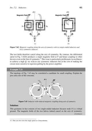
![466 Chap. 7. Passive Devices
Example 7.21 (Continued)
The structure is more symmetric than the single-ended spirals with step symmetry in
Fig. 7.42(a). Unfortunately, the Q of this topology is lower than that of a differential induc-
tor because each half experiences its own substrate loss; i.e., the doubling of the substrate
shunt resistance observed in Fig. 7.37 does not occur here. A variant of this structure is
described in [12].
Inductors with Ground Shield In our early study of substrate loss in Section 7.2.5, we
contemplated the use of a grounded shield below the inductor. The goal was to allow the
displacement current to flow through a low resistance to ground, thus avoiding the loss due
to electric coupling to the substrate. But we observed that eddy currents in a continuous
shield drastically reduce the inductance and the Q.
We now observe that the shield can provide a low-resistance termination for electric
field lines even if it is not continuous. As illustrated in Fig. 7.44 [13], a “patterned” shield,
i.e., a plane broken periodically in the direction perpendicular to the flow of eddy currents,
receives most of the electric field lines without reducing the inductance. A small fraction
of the field lines sneak through the gaps in the shield and terminate on the lossy substrate.
Thus, the width of the gaps must be minimized.
Broken
Shield
Displacement
Current
Figure 7.44 Inductor with patterned ground shield.
It is important to note that the patterned ground shield only reduces the effect of capaci-
tive coupling to the substrate. The eddy currents resulting from magnetic coupling continue
to flow through the substrate as Faraday and Lenz have prescribed.
Example 7.22
A student designing a patterned ground shield decides that minimizing the gap width is not
a good idea because it increases the capacitance between each two sections of the shield,
potentially allowing large eddy currents to flow through the shield. Is the student correct?
Solution:
While it is true that the gap capacitance increases, we must note that all of the gap capac-
itances appear in series with the path of eddy currents. The overall equivalent capacitance
is therefore very small and the impedance presented to eddy currents quite high.](https://image.slidesharecdn.com/rfmicroelectronicsrazavi-230814101614-71259b59/85/RF-MICROELECTRONICS_Razavi-pdf-491-320.jpg)
![Sec. 7.2. Inductors 467
The use of a patterned shield may increase the Q by 10 to 15% [13], but this improve-
ment depends on many factors and has thus been inconsistent in different reports [14]. The
factors include single-ended versus differential operation, the thickness of the metal, and
the resistivity of the substrate. The improvement comes at the cost of higher capacitance.
For example, if the inductor is realized in metal 9 and the shield in metal 1, then the capaci-
tance rises by about 15%. One can utilize a patterned n1 region in the substrate as the shield
to avoid this capacitance increase, but the measurement results have not been consistent.
The other difficulty with patterned shields is the additional complexity that they intro-
duce in modeling and layout. The capacitance to the shield and the various losses now
require much lengthier electromagnetic simulations.
Stacked Inductors At frequencies up to about 5 GHz, inductor values encountered in
practice fall in the range of five to several tens of nanohenries. If realized as a single spiral,
such inductors occupy a large area and lead to long interconnects between the circuit blocks.
This issue can be resolved by exploiting the third dimension, i.e., by stacking spirals. Illus-
trated in Fig. 7.45, the idea is to place two or more spirals in series, obtaining a higher
inductance not only due to the series connection but also as a result of strong mutual
coupling. For example, the total inductance in Fig. 7.45 is given by
Ltot 5 L1 1 L2 1 2M. (7.76)
Since the lateral dimensions of L1 and L2 are much greater than their vertical separation,
L1 and L2 exhibit almost perfect coupling, i.e., M ≈ L1 5 L2 and Ltot ≈ 4L1. Similarly, n
stacked spirals operating in series raise the total inductance by approximately a factor of n2.
L1
L2
Metal 9
Metal 8
I
I
Figure 7.45 Stacked spirals.
Example 7.23
The five-turn 4.96-nH inductor obtained from Eq. (7.15) in Section 7.2.3 has an outer
dimension of
Dout 5
ltot
4N
1 W 1 (N 2 1)(W 1 S) (7.77)
5 122 μm. (7.78)
Using Eq. (7.15) for the inductance of one spiral, determine the required outer dimension
of a four-turn stacked structure having the same W and S. Assume two spirals are stacked.
(Continues)](https://image.slidesharecdn.com/rfmicroelectronicsrazavi-230814101614-71259b59/85/RF-MICROELECTRONICS_Razavi-pdf-492-320.jpg)
![468 Chap. 7. Passive Devices
Example 7.23 (Continued)
Solution:
Each spiral must provide an inductance of 4.96 nH/4 5 1.24 nH. Iteration with N 5 4,
W 5 4 μm, and S 5 0.5 μm in Eq. (7.15) yields ltot ≈ 780 μm and hence Dout 5 66.25 μm.
Stacking thus reduces the outer dimension by nearly a factor of 2 in this case.
(a) (b)
C1
C2
Substrate
L1
L2
C1
C2
Substrate
L1
L2
Metal 9
Metal 8
Metal 9
Metal 5
Figure 7.46 Equivalent capacitance for a stack of (a) metal-9 and metal-8, or (b) metal-9 and
metal-5 spirals.
In reality, the multiplication factor of stacked square inductors is less than n2 because
the legs of one inductor that are perpendicular to the legs of the other provide no mutual
coupling. For example, a stack of two raises the inductance by about a factor of 3.5 [6].
The factor is closer to n2 for octagonal spirals and almost equal to n2 for circular structures.
In addition to the capacitance to the substrate and the interwinding capacitance, stacked
inductors also contain one between the spirals [Fig. 7.46(a)].
Example 7.24
In most circuits, one terminal of the inductor(s) is at ac ground. Which terminal of the
structure in Fig. 7.46(a) should be grounded?
Solution:
Since L2 sees a much larger capacitance to the substrate than L1 does, the terminal of L2
should be grounded. This is a critical point in the use of stacked inductors.
Using an energy-based analysis similar to that in Section 7.2.4, [6] proves that the
equivalent lumped capacitance of the inductor shown in Fig. 7.46(a) is equal to
Ceq 5
4C1 1 C2
12
, (7.79)](https://image.slidesharecdn.com/rfmicroelectronicsrazavi-230814101614-71259b59/85/RF-MICROELECTRONICS_Razavi-pdf-493-320.jpg)
![Sec. 7.2. Inductors 469
if the free terminal of L2 is at ac ground.12
Interestingly, the inter-spiral capacitance has a
larger weighting factor than the capacitance to the substrate does. For this reason, if L2 is
moved to lower metal layers [Fig. 7.46(b)], Ceq falls even though C2 rises. Note that the
total inductance remains approximately constant so long as the lateral dimensions are much
greater than the vertical spacing between L1 and L2.
Example 7.25
Compare the equivalent lumped capacitance of single-layer and stacked 4.96-nH induc-
tors studied in Example 7.23. Assume the lower spiral is realized in metal 5 and use the
capacitance values shown in Table 7.1.
Table 7.1 Table of metal capacitances (aF/μm2).
Metal 8 Metal 7 Metal 6 Metal 5 Substrate
Metal 9 52 16 12 9.5 4.4
Metal 8 52 24 16 5.4
Metal 7 88 28 6.1
Metal 6 88 7.1
Metal 5 8.6
Solution:
For a single metal-9 layer, the total area is equal to 2000 μm 3 4 μm 5 8000 μm2, yielding
a total capacitance of 35.2 fF to the substrate. As suggested by Eq. (7.26), the equivalent
lumped capacitance is 1/3 of this value, 11.73 fF. For the stacked structure, each spiral has
an area of 780 μm 3 4 μm 5 3120 μm2. Thus, C1 5 29.64 fF and C2 5 26.83 fF, resulting
in
Ceq 5 12.1 fF. (7.80)
The choice of stacking therefore translates to comparable capacitances.13
If L2 is moved
down to metal 4 or 3, the capacitance of the stacked structure falls more.
For n stacked spirals, it can be proved that
Ceq 5
4
n21
m 5 1
Cm 1 Csub
3n2
, (7.81)
where Cm denotes each inter-spiral capacitance [6].
12. If the free terminal of L1 is grounded, the equivalent capacitance is quite larger.
13. We have neglected the fringe components for simplicity.](https://image.slidesharecdn.com/rfmicroelectronicsrazavi-230814101614-71259b59/85/RF-MICROELECTRONICS_Razavi-pdf-494-320.jpg)
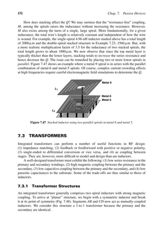
![Sec. 7.3. Transformers 471
A C A C
D B
Figure 7.48 Transformer derived from a symmetric inductor.
Example 7.26
What is the relationship between the inductance of the symmetric spiral of Fig. 7.48 and
the inductances of the resulting transformer?
Solution:
We have
LAC 5 LAB 1 LCD 1 2M, (7.82)
where each L refers to the inductance between its end points and M to the mutual coupling
between LAB and LDC. Since LAB 5 LCD,
LAC 5 2LAB 1 2M. (7.83)
If LAC and M are known, we can determine the inductance of the primary and the secondary.
The transformer structure of Fig. 7.48 suffers from low magnetic coupling, an asym-
metric primary, and an asymmetric secondary. To remedy the former, the number of turns
can be increased [Fig. 7.49(a)] but at the cost of higher capacitive coupling. To remedy the
latter, two symmetric spirals can be embedded as shown in Fig. 7.49(b) but with a slight
A C A
B D
B
C D
(a (
) b)
Figure 7.49 Transformers (a) derived from a three-turn symmetric inductor, (b) formed as two
embedded symmetric spirals.](https://image.slidesharecdn.com/rfmicroelectronicsrazavi-230814101614-71259b59/85/RF-MICROELECTRONICS_Razavi-pdf-496-320.jpg)
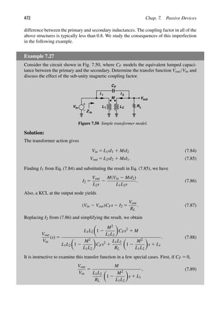
![Sec. 7.3. Transformers 473
Example 7.27 (Continued)
suggesting that, since k 5 M/
√
L1L2 1, the transformer exhibits a low-pass response
with a real pole located at
ωp 5
2RL
L2
1 2
M2
L1L2
. (7.90)
For example, if k 5 0.7, then ωp 5 21.96RL/L2. This pole must lie well above the
frequency of operation.
Second, if CF 0 but M 5 L1 5 L2, then Vout/Vin 5 M/L1 5 1 regardless of the val-
ues of CF and RL. Thus, CF manifests itself because of the sub-unity k. Since typically
L1 5 L2 5 L, we can express the poles of Eq. (7.88) as
ωp1,2 5
1
2RLCF
⎡
⎣21 ±
1 2
4R2
LCF
L(1 2 k2)
⎤
⎦ . (7.91)
Equation (7.88) implies that it is beneficial to reduce L1 and L2 while k remains
constant; as L1 and L2 (and M 5 k
√
L1L2) approach zero,
Vout
Vin
(s) ≈
M
L1
, (7.92)
a frequency-independent quantity equal to k if L1 5 L2. However, reduction of L1 and L2
also lowers the input impedance, Zin, in Fig. 7.50. For example, if CF 5 0, we have from
Eq. (7.54),
Zin 5 L1s 2
M2s2
RL 1 L2s
. (7.93)
Thus, the number of primary and secondary turns must be chosen so that Zin is adequately
high in the frequency range of interest.
Is it possible to construct planar transformers having a turns ratio greater than unity?
Figure 7.51(a) shows an example, where AB has approximately one turn and CD approx-
imately two. We note, however, that the mutual coupling between AB and the inner
turn of CD is relatively weak due to the smaller diameter of the latter. Figure 7.51(b)
depicts another 1-to-2 example with a stronger coupling factor. In practice, the primary
and secondary may require a larger number of turns so as to provide a reasonable input
impedance.
Figure 7.52 shows two other examples of planar transformers. Here, two asymmetric
spirals are interwound to achieve a high coupling factor. The geometry of Fig. 7.52(a) can
be viewed as two parallel conductors that are wound into turns. Owing to the difference
between their lengths, the primary and secondary exhibit unequal inductances and hence
a nonunity turns ratio [16]. The structure of Fig. 7.52(b), on the other hand, provides an
exact turns ratio of unity [16].
Transformers can also be implemented as three-dimensional structures. Similar to the
stacked inductors studied in Section 7.2.7, a transformer can employ stacked spirals for the](https://image.slidesharecdn.com/rfmicroelectronicsrazavi-230814101614-71259b59/85/RF-MICROELECTRONICS_Razavi-pdf-498-320.jpg)
![474 Chap. 7. Passive Devices
(a) (b)
A B
C D
A
C
D
B
Figure 7.51 One-to-two transformers (a) derived from a symmetric inductor, (b) formed as two
symmetric inductors.
A
B
C
D
A
B
C
D
(a) (b)
Figure 7.52 (a) Transformer formed as two wires wound together, (b) alternative version with equal
primary and secondary lengths.
Secondary
Primary
Metal 9
Metal 7
Metal 5
Secondary
Primary
Metal 9
Metal 7
Secondary
Primary
(a) (b) (c)
Figure 7.53 (a) One-to-one stacked transformer, (b) one-to-two transformer, (c) staggering of turns
to reduce coupling capacitance.
primary and the secondary [6]. Figure 7.53(a) shows a 1-to-1 example. It is important to
recognize the following attributes: (1) the alignment of the primary and secondary turns
results in a slightly higher magnetic coupling factor here than in the planar transformers of
Figs. 7.49 and 7.51; (2) unlike the planar structures, the primary and the secondary can be](https://image.slidesharecdn.com/rfmicroelectronicsrazavi-230814101614-71259b59/85/RF-MICROELECTRONICS_Razavi-pdf-499-320.jpg)
![Sec. 7.3. Transformers 475
symmetric and identical (except for differences in their capacitances); (3) the overall area
occupied by 3D transformers is less than that of their planar counterparts.
Another advantage of stacked transformers is that they can readily provide a turns
ratio higher than unity [6]. Illustrated in Fig. 7.53(b), the idea is to incorporate multiple
spirals in series to form the primary or the secondary. Thus, a technology having nine
metal layers can afford 1-to-8 transformers! As shown in [6], stacked transformers indeed
provide significant voltage or current gain at gigahertz frequencies. This “free” gain can be
utilized between stages in a chain.
Stacked transformers must, however, deal with two issues. First, the lower spirals suffer
from a higher resistance due to the thinner metal layers. Second, the capacitance between
the primary and secondary is larger here than in planar transformers (why?). To reduce this
capacitance, the primary and secondary turns can be “staggered,” thus minimizing their
overlap [Fig. 7.53(c)] [6]. But this requires a relatively large spacing between the adjacent
turns of each inductor, reducing the inductance.
7.3.2 Effect of Coupling Capacitance
The coupling capacitance between the primary and secondary yields different types of
behavior with negative and positive mutual (magnetic) coupling factors. To understand
this point, we return to the transfer function in Eq. (7.88) and note that, for s 5 jω, the
numerator reduces to
N(jω) 5 2 L1L2
1 2
M2
L1L2
CFω2
1 M. (7.94)
The first term is always negative, but the polarity of the second term depends on the
direction chosen for mutual coupling. Thus, if M 0, then N(jω) falls to zero at
ωz 5
M
L1L2
1 2
M2
L1L2
CF
, (7.95)
i.e., the frequency response exhibits a notch at ωz. On the other hand, if M 0, no
such notch exists and the transformer can operate at higher frequencies. We therefore
say “noninverting” transformers suffer from a lower speed than do “inverting” transfor-
mers [16].
The above phenomenon can also be explained intuitively: the feedforward signal
through CF can cancel the signal coupled from L1 to L2. Specifically, the voltage across
L2 in Fig. 7.50 contains two terms, namely, L2jωI2 and MjωI1. If, at some frequency, I2 is
entirely provided by CF, the former term can cancel the latter, yielding a zero output voltage.
7.3.3 Transformer Modeling
An integrated transformer can be viewed as two inductors having magnetic and capac-
itive coupling. The inductor models described in Section 7.2.6 therefore directly apply
here. Figure 7.54 shows an example, where the primary and secondary are represented
by the compact inductor model of Fig. 7.35(b), with the mutual coupling M and coupling
capacitor CF added. More details on transformer modeling can be found in [16] and [17].](https://image.slidesharecdn.com/rfmicroelectronicsrazavi-230814101614-71259b59/85/RF-MICROELECTRONICS_Razavi-pdf-500-320.jpg)
![476 Chap. 7. Passive Devices
L1 L2
M
C
C
F
F
Figure 7.54 Transformer model.
Due to the complexity of this model, it is difficult to find the value of each component from
measurements or field simulations that provide only S- or Y-parameters for the entire struc-
ture. In practice, some effort is expended on this type of modeling to develop insight into
the transformer’s limitations, but an accurate representation may require that the designer
directly use the S- or Y-parameters in circuit simulations. Unfortunately, circuit simulators
sometimes face convergence difficulties with these parameters.
7.4 TRANSMISSION LINES
Integrated transmission lines (T-lines) are occasionally used in RF design. It is instructive to
consider a few examples of T-line applications. Suppose a long wire carries a high-frequency
signal from one circuit block to another (Fig. 7.55). The wire suffers from inductance,
capacitance, and resistance. If the width of the wire is increased so as to reduce the induc-
tance and series resistance, then the capacitance to the substrate rises. These parasitics may
considerably degrade the signal as the frequency exceeds several gigahertz.
Block
A
Block
B
Y
X
Figure 7.55 Two circuit blocks connected by a long wire.
Example 7.28
For the wire shown in Fig. 7.55, we also say the current “return path” is poorly-defined.
Explain this attribute and its consequences.
Solution:
In the ideal situation, the signal current flowing through the wire from block A to block B
returns through a ground plane [Fig. 7.56(a)]. In reality, however, due to the wire parasitics](https://image.slidesharecdn.com/rfmicroelectronicsrazavi-230814101614-71259b59/85/RF-MICROELECTRONICS_Razavi-pdf-501-320.jpg)
![Sec. 7.4. Transmission Lines 477
Example 7.28 (Continued)
and the nonideal ground connection between the two blocks, some of the signal current
flows through the substrate [Fig. 7.56(b)]. The complexity of the return path makes it dif-
ficult to accurately predict the behavior of the wire at high frequencies. Also, the coupling
to the substrate creates leakage of the signal to other parts of the chip.
Block
A
Block
B
Y
X
I 1
I
GND
Block
A
Block
B
Y
X
I 1
Substrate
(a) (b)
1
Figure 7.56 (a) Current return path through a ground plane, (b) poor definition of current return
path.
If the long wire in Fig. 7.55 is replaced with a T-line and the input port of block B is
modified to match the T-line, then the above issues are alleviated. As illustrated in Fig. 7.57,
the line inductance and capacitance no longer degrade the signal, and the T-line ground
plane not only provides a low-impedance path for the returning current but minimizes the
interaction of the signal with the substrate. The line resistance can also be lowered but with
a trade-off (Section 7.4.1).
Block
A
Block
B
Z0
RT Z0
=
Z 0
Figure 7.57 Two circuit blocks connected by a T-line.
As another example of T-line applications, recall from Chapter 2 that a T-line having a
short-circuit termination acts as an inductor if it is much shorter than a wavelength. Thus,
T-lines can serve as inductive loads (Fig. 7.58).
VDD
out
V
in
V M 1
Z0
d
Figure 7.58 T-line serving as a load inductor.](https://image.slidesharecdn.com/rfmicroelectronicsrazavi-230814101614-71259b59/85/RF-MICROELECTRONICS_Razavi-pdf-502-320.jpg)
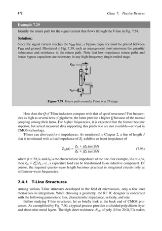
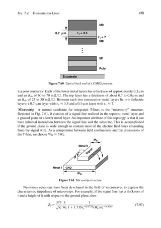
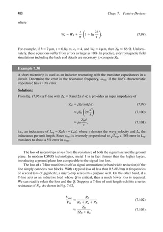
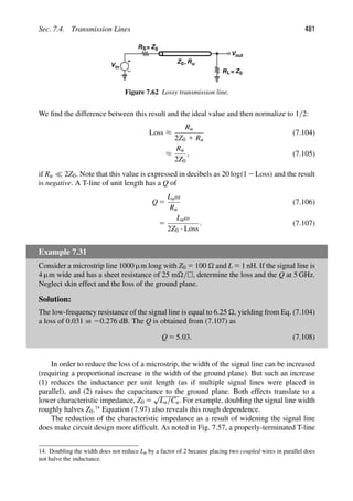
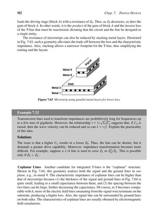
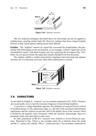
![484 Chap. 7. Passive Devices
n−well
+
p
−substrate
p
+
n +
p
−substrate
p
+
n
(a (
) b)
+
p +
n
Side
View
View
Top
+
p +
n
Figure 7.66 PN junction varactor with (a) one terminal grounded, (b) both terminals floating.
the substrate.) In this case, the anode is “hard-wired” to ground, limiting the design flexi-
bility. A “floating” pn junction can be constructed as shown in Fig. 7.66(b), with an n-well
isolating the diode from the substrate and acting as the cathode.
Let us examine the capacitance range and Q of pn junctions. At a reverse bias of VD,
the junction capacitance, Cj, is given by
Cj 5
Cj0
1 1
VD
V0
m , (7.109)
where Cj0 is the capacitance at zero bias, V0 the built-in potential, and m an exponent
around 0.3 in integrated structures. We recognize the weak dependence of Cj upon VD.
Since V0 ≈ 0.7 to 0.8 V and since VD is constrained to less than 1 V by today’s supply
voltages, the term 1 1 VD/V0 varies between approximately 1 and 2. Furthermore, an m of
about 0.3 weakens this variation, resulting in a capacitance range, Cj,max/Cj,min, of roughly
1.23. In practice, we may allow the varactor to experience some forward bias (0.2 to 0.3 V),
thus obtaining a somewhat larger range.
The Q of a pn-junction varactor is given by the total series resistance of the structure.
In the floating diode of Fig. 7.66(b), this resistance is primarily due to the n-well and can be
minimized by selecting minimum spacing between the n1 and p1 contacts. Moreover, as
shown in Fig. 7.67, each p1 region can be surrounded by an n1 ring to lower the resistance
in two dimensions.
Unlike inductors, transformers, and T-lines, varactors are quite difficult to simulate and
model, especially for Q calculations. Consider the displacement current flow depicted in
Fig. 7.68(a). Due to the two-dimensional nature of the flow, it is difficult to determine or
compute the equivalent series resistance of the structure. This issue arises partly because
the sheet resistance of the n-well is typically measured by the foundry for contacts having a
spacing greater than the depth of the n-well [Fig. 7.68(b)]. Since the current path in this case
is different from that in Fig. 7.68(a), the n-well sheet resistance cannot be directly applied](https://image.slidesharecdn.com/rfmicroelectronicsrazavi-230814101614-71259b59/85/RF-MICROELECTRONICS_Razavi-pdf-509-320.jpg)
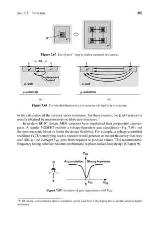
![486 Chap. 7. Passive Devices
n−well
−substrate
p
+
n
+
n
VG
VS
n−well
−substrate
p
VG
VS
+
n
+
n
n−well
−substrate
p
VG
VS
+
n
+
n
Depletion
Region
−−−−−−−−−
Accumulation
Layer
(c)
(a) b)
V
CGS
0 GS
(d)
Cmin
Cmax
(
Figure 7.70 (a) MOS varactor, (b) operation with negative gate-source voltage, (c) operation with
positive gate-source voltage, (d) resulting C/V characteristic.
A simple modification of the MOS device avoids the above issues. Called an
“accumulation-mode MOS varactor” and shown in Fig. 7.70(a), this structure is obtained
by placing an NMOS transistor inside an n-well. If VG VS, then the electrons in the n-well
are repelled from the silicon/oxide interface and a depletion region is formed [Fig. 7.70(b)].
Under this condition, the equivalent capacitance is given by the series combination of the
oxide and depletion capacitances. As VG exceeds VS, the interface attracts electrons from
the n1 source/drain terminals, creating a channel [Fig. 7.70(c)]. The overall capacitance
therefore rises to that of the oxide, behaving as shown in Fig. 7.70(d). (Since the material
under the gate is n-type silicon, the concept of strong inversion does not apply here.)
The C/V characteristic of MOS varactors has scaled well with CMOS technology gen-
erations, approaching its saturated levels of Cmax and Cmin for VGS ≈ ±0.5 V in 65-nm
devices. These varactors therefore operate with low supply voltages better than their
pn-junction counterparts.
Another advantage of accumulation-mode MOS varactors is that, unlike pn junc-
tions, they can tolerate both positive and negative voltages. In fact, the characteristic of
Fig. 7.70(d) suggests that MOS varactors should operate with positive and negative biases
so as to provide maximum tuning range. We pursue this point in VCO design in Chapter 8.
Circuit simulations must somehow incorporate the varactor C/V characteristic of
Fig. 7.70(d). In practice, this characteristic is measured on fabricated devices and repre-
sented by a table of discrete values. Such a table, however, may introduce discontinuities in
the derivatives of the characteristic, creating undesirable artifacts (e.g., a high noise floor)
in simulations. It is therefore desirable to approximate the C/V plot by a well-behaved](https://image.slidesharecdn.com/rfmicroelectronicsrazavi-230814101614-71259b59/85/RF-MICROELECTRONICS_Razavi-pdf-511-320.jpg)
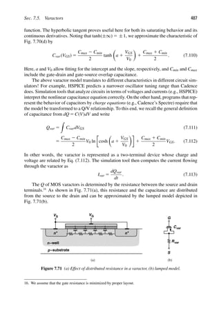
![488 Chap. 7. Passive Devices
Example 7.33
Determine the equivalent resistance and capacitance values in the lumped model of
Fig. 7.71(b).
Cu Cu
Ru
Cu
Ru
Ru
V
Cu Cu
Ru
Cu
Ru
Ru Ru
Ctot
Rtot
X
I X
Ru Ru
Ru
VX
I X
Cu Cu Cu
Z in
Z 1
1
Y
Z 1
1
Y
Z 1
1
Y
Z in
(c)
(a)
(b)
Figure 7.72 (a) Distributed model of a varactor, (b) equivalent circuit for half of the structure,
(c) canonical T-line structure.
Solution:
Let us first consider only one-half of the structure as shown in Fig. 7.72(a). Here, the unit
capacitances add up to the total distributed capacitance, Ctot, and the unit resistances to
the total distributed resistance, Rtot. We turn the circuit upside down, arriving at the more
familiar topology illustrated in Fig. 7.72(b). The circuit now resembles a transmission line
consisting of series resistances and parallel capacitances. For the general T-line shown in
Fig. 7.72(c), it can be proved that the input impedance, Zin, is given by [18]
Zin 5
Z1
Y1
1
tanh(
√
Z1Y1d)
, (7.114)
where Z1 and Y1 are specified for unit length and d is the length of the line. From
Fig. 7.72(b), Z1d 5 Rtot and Y1d 5 Ctots; thus,
Zin 5
Rtot
Ctots
1
tanh(
√
RtotCtots/4)
. (7.115)
At frequencies well below 1/(RtotCtot/4), the argument of tanh is much less than unity,
allowing the approximation,
tanh ≈ 2
3
3
(7.116)
≈
1 1
2
3
. (7.117)](https://image.slidesharecdn.com/rfmicroelectronicsrazavi-230814101614-71259b59/85/RF-MICROELECTRONICS_Razavi-pdf-513-320.jpg)
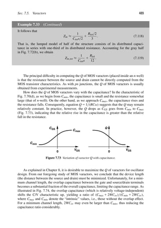
![490 Chap. 7. Passive Devices
V
CGS
0 GS
Cmin
Cmax
Cmin + 2WCov
C + 2WCov
max
With Overlap
Capacitance
Capacitance
Without Overlap
Figure 7.74 Effect of overlap capacitance on varactor capacitance range.
Example 7.34
A MOS varactor realized in 65-nm technology has an effective length of 50 nm and a Cov of
0.09 fF/μm. If Cox 5 17 fF/μm2, determine the largest capacitance range that the varactor
can provide.
Solution:
Assuming a width of 1 μm for the device, we have 2WCov 5 0.18 fF and a gate oxide
capacitance of 17 fF/μm2 3 1 μm 3 50 nm 5 0.85 fF. Thus, the minimum capacitance is
0.18 fF (if the series combination of the oxide and depletion capacitances is neglected),
and the maximum capacitance reaches 0.85 fF 1 0.18 fF 5 1.03 fF. The largest possible
capacitance ratio is therefore equal to 5.72. In practice, the series combination of the oxide
and depletion capacitances is comparable to 2WCov, reducing this ratio to about 2.5.
In order to achieve a larger capacitance range, the length of MOS varactors can be
increased. In the above example, if the effective channel length grows to 100 nm, then the
capacitance ratio reaches (1.7 fF 1 0.18 fF)/(0.18 fF) 5 10.4. However, the larger source-
drain resistance results in a lower Q. Since the maximum capacitance goes from 1.03 fF to
1.88 fF and since the channel resistance is doubled, the Q [ 5 1/(RCω)] falls by a factor
of 3.65. In other words, an m-fold increase in the channel length translates to roughly an
m2-fold drop in the Q.
The trade-off between the capacitance range and Q of varactors ultimately leads to
another between the tuning range and phase noise of LC VCOs. We study this issue in
Chapter 8. At frequencies up to about 10 GHz, a channel length of twice the minimum may
be chosen so as to widen the capacitance range while retaining a varactor Q much larger
than the inductor Q.
7.6 CONSTANT CAPACITORS
RF circuits employ constant capacitors for various purposes, e.g., (1) to adjust the reso-
nance frequency of LC tanks, (2) to provide ac coupling between stages, or (3) to bypass
the supply rail to ground. The critical parameters of capacitors used in RF ICs include the](https://image.slidesharecdn.com/rfmicroelectronicsrazavi-230814101614-71259b59/85/RF-MICROELECTRONICS_Razavi-pdf-515-320.jpg)
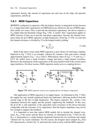
![492 Chap. 7. Passive Devices
Example 7.35
A MOS capacitor can be constructed as a single transistor of length L [Fig. 7.76(a)]
or N transistors in parallel, each of length L/N. Compare the Q’s of the two struc-
tures. For simplicity, assume the effective channel lengths are equal to L and L/N,
respectively.
Solution:
The structure of Fig. 7.76(a) exhibits a channel resistance of
Ron,a 5
1
μnCox
W
L
(VGS 2 VTH)
, (7.121)
and each finger in Fig. 7.76(b) a channel resistance of
Ron,u 5
1
μnCox
W
L/N
(VGS 2 VTH)
, (7.122)
Since N fingers appear in parallel, Ron,b 5 Ron,u/N 5 Ron,a/N2. That is, the decomposition
of the device into N parallel fingers reduces the resistance by a factor of N2.
L
W
L
W
N
S
D
(a) (b)
Figure 7.76 MOS capacitor realized as (a) one long finger, (b) multiple short fingers.
For frequencies up to a few tens of gigahertz, the above decomposition can yield
reasonable Q’s (e.g., 5 to 10), allowing the use of MOS capacitors for supply bypass.
The reader is cautioned that very large MOS capacitors suffer from significant gate
leakage current, especially with a VGS as high as VDD. This current manifests itself if the
system must enter a low-power (standby) mode: the leakage persists as long as VDD is
applied, draining the battery.](https://image.slidesharecdn.com/rfmicroelectronicsrazavi-230814101614-71259b59/85/RF-MICROELECTRONICS_Razavi-pdf-517-320.jpg)
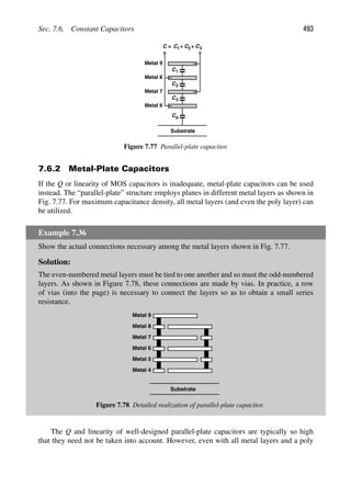
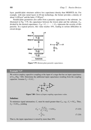
![References 495
C C C
f1 f2 fn
Figure 7.81 Fringe capacitor structure.
To alleviate the above issue, only a few top metal layers can be utilized. For example, a
structure consisting of metal 9 through metal 4 has a density of 660 aF/μm2 and a parasitic
of 18 aF/μm2, i.e., 2.7%. Of course, the lower density translates to a larger area and more
complex routing of signals.
An alternative geometry utilizes the lateral electric field between adjacent metal lines to
achieve a high capacitance density. Illustrated in Fig. 7.81, this “fringe” capacitor consists
of narrow metal lines with the minimum allowable spacing. This structure is described in
Chapter 8.
REFERENCES
[1] J. Craninckx and M. S. J. Steyaert, “A 1.8 GHz CMOS Low Phase Noise Voltage-Controlled
Oscillator with Prescaler,” IEEE Journal of Solid-State Circuits, vol. 30, pp. 1474–1482, Dec.
1995.
[2] S. Jenei, B. K. J. C. Nauwelaers, and S. Decoutere, “Physics-Based Closed-Form Inductance
Expressions for Compact Modeling of Integrated Spiral Inductors,” IEEE Journal of Solid-
State Circuits, vol. 37, pp. 77–80, Jan. 2002.
[3] S. S. Mohan et al., “Simple Accurate Expressions for Planar Spiral Inductances,” IEEE
J. Solid-State Circuits, vol. 34, pp. 1419–1424, Oct. 1999.
[4] A. Niknejad and R. G. Meyer, “Analysis, Design, and Optimization of Spiral Inductors and
Transformers for Si RF ICs,” IEEE J. Solid-State Circuits, vol. 33, pp. 1470–1481, Oct. 1998.
[5] M. Kraemer, D. Dragomirescu, and R. Plana, “Accurate Electromagnetic Simulation and Mea-
surement of Millimeter-Wave Inductors in Bulk CMOS Technology,” IEEE Topical Meeting
on Silison Monolithic Integrated Circuits in RF Systems, pp. 61–64, Jan. 2010.
[6] A. Zolfaghari, A. Y. Chan, and B. Razavi, “Stacked Inductors and 1-to-2 Transformers in
CMOS Technology,” IEEE Journal of Solid-State Circuits, vol. 36, pp. 620–628, April 2001.
[7] W. B. Kuhn, “Approximate Analytical Modeling of Current Crowding Effects in Multi-Turn
Spiral Inductors,” IEEE RFIC Symp. Dig. Tech. Papers, pp. 271–274, June 2000.
[8] W. B. Kuhn and N. M. Ibrahim, “Analysis of Current Crowding Effects in Multiturn Spiral
Inductors,” IEEE Tran. MTT, vol. 49, pp. 31–39, Jan. 2001.
[9] C. S. Yen, Z. Fazarinc, and R. Wheeler, “Time-Domain Skin-Effect Model for Transient
Analysis of Lossy Transmission Lines,” Proc. of IEEE, vol. 70, pp. 750–757, July 1982.
[10] Y. Cao et al., “Frequency-Independent Equivalent Circuit Model of On-Chip Spiral Inductors,”
Proc. CICC, pp. 217–220, May 2002.
[11] M. Danesh et al., “A Q-Factor Enhancement Technique for MMIC Inductors,” Proc. IEEE
Radio Frequency Integrated Circuits Symp., pp. 217–220, April 1998.
[12] N. M. Neihart et al., “Twisted Inductors for Low Coupling Mixed-signal and RF Applica-
tions,” Proc. CICC, pp. 575–578, Sept. 2008.](https://image.slidesharecdn.com/rfmicroelectronicsrazavi-230814101614-71259b59/85/RF-MICROELECTRONICS_Razavi-pdf-520-320.jpg)
![496 Chap. 7. Passive Devices
[13] C. P. Yue and S. S. Wong, “On-Chip Spiral Inductors with Patterned Ground Shields for
Si-Based RF ICs,” IEEE J. Solid-State Circuits, vol. 33, pp. 743–751, May 1998.
[14] S.-M. Yim, T. Chen, and K. K. O, “The Effects of a Ground Shield on the Characteristics and
Performance of Spiral Inductors,” IEEE J. Solid-State Circuits, vol. 37, pp. 237–245, Feb.
2002.
[15] Y. E. Chen et al., “Q-Enhancement of Spiral Inductor with N1-Diffusion Patterned Ground
Shields,” IEEE MTT Symp. Dig. Tech. Papers, pp. 1289–1292, 2001.
[16] J. R. Long, “Monolithic Transformers for Silicon RF IC Design,” IEEE J. Solid-State Circuits,
vol. 35, pp. 1368–1383, Sept. 2000.
[17] J. R. Long and M. A. Copeland, “The Modeling, Characterization, and Design of Monolithic
Inductors for Silicon RF ICs,” IEEE J. Solid-State Circuits, vol. 32, pp. 357–369, March 1997.
[18] S. Ramo, J. R. Whinnery, and T. Van Duzer, Fields and Waves in Communication Electronics,
Third Edition, New York: Wiley, 1994.
PROBLEMS
7.1. Extend Eq. (7.1) to an N-turn spiral and show that Ltot contains N(N 1 1)/2 terms.
7.2. Prove that the Q of the circuit shown in Fig. 7.32(a) is given by Eq. (7.62).
7.3. Prove that for an N-turn spiral inductor, the equivalent interwinding capacitance is
given by
Ceq 5
C1 1 · · · 1 CN221
(N2 2 1)2
. (7.125)
7.4. Using Eq. (7.62), compare the Q’s of the circuits shown in Figs. 7.37(b) and (d).
7.5. Consider the magnetic fields produced by the inductors in Fig. 7.41. Which topol-
ogy creates less net magnetic field at a point far from the circuit but on its line of
symmetry?
7.6. Repeat Example 7.13 for a 5-nH inductor using a linewidth of 5 μm, a line spacing
of 0.5 μm, and four turns. Do the results depend much on the outer diameter?
7.7. For the circuit of Fig. 7.28(a), compute Y11 and find the parallel equivalent resistance.
Is the result the same as that shown in Eq. (7.55)?
7.8. Repeat Example 7.19 for four turns. Is it possible to find an expression for N turns?
7.9. Find the input impedance, Zin, in Fig. 7.50.
7.10. Using the capacitance data in Table 7.1, repeat Example 7.25 for an inductor realized
as a stack of four metal layers. Assume the inductance is about 3.5 times that of one
spiral.
7.11. Suppose an LC VCO (Chapter 8) employs pn-junction varactors. Determine the
bounds on the control voltage and the output swings if the varactors must remain
reverse-biased.](https://image.slidesharecdn.com/rfmicroelectronicsrazavi-230814101614-71259b59/85/RF-MICROELECTRONICS_Razavi-pdf-521-320.jpg)
![498 Chap. 8. Oscillators
Example 8.1
A direct-conversion transceiver is designed for the 2.4-GHz and 5-GHz wireless bands. If
a single LO must cover both bands, what is the minimum acceptable tuning range?
Solution:
Figure 8.1 shows a possible arrangement for covering both bands. For the lower band,
4.8 GHz ≤ fLO ≤ 4.96 GHz. Thus, we require a total tuning range of 4.8 GHz to 5.8 GHz,
about 20%. Such a wide tuning range is relatively difficult to achieve in LC oscillators.
LO
f
11a TRX
LO
2
11b/g TRX
5.2−5.8 GHz
2.40−2.48 GHz
Figure 8.1 LO path of a dual-band transceiver.
The actual frequency range of an oscillator may also depend on whether quadrature
outputs are required and/or injection pulling is of concern (Chapter 4). A direct-conversion
transceiver employs quadrature phases of the carrier, necessitating that either the oscillator
directly generate quadrature outputs or it run at twice the required frequency so that a ÷2
stage can produce such outputs. For example, in the hybrid topology of Fig. 8.1, the LO
must still provide quadrature phases in the 5-GHz range—but it is prone to injection pulling
by the PA output. We address the problem of quadrature generation in Section 8.11.
How high a frequency can one expect of a CMOS oscillator? While oscillation fre-
quencies as high as 300 GHz have been demonstrated [1], in practice, a number of serious
trade-offs emerge that become much more pronounced at higher operation frequencies. We
analyze these trade-offs later in this chapter.
Output Voltage Swing As exemplified by the arrangement shown in Fig. 8.1, the oscil-
lators in an RF system drive mixers and frequency dividers. As such, they must produce
sufficiently large output swings to ensure nearly complete switching of the transistors in the
subsequent stages. Furthermore, as studied in Section 8.7, excessively low output swings
exacerbate the effect of the internal noise of the oscillator. With a 1-V supply, a typical
single-ended swing may be around 0.6 to 0.8 Vpp. A buffer may follow the oscillator to
amplify the swings and/or drive the subsequent stage.
Drive Capability Oscillators may need to drive a large load capacitance. Figure 8.2
depicts a typical arrangement for the receive path. In addition to the downconversion mix-
ers, the oscillator must also drive a frequency divider, denoted by a ÷N block. This is
because a loop called the “frequency synthesizer” must precisely control the frequency of](https://image.slidesharecdn.com/rfmicroelectronicsrazavi-230814101614-71259b59/85/RF-MICROELECTRONICS_Razavi-pdf-523-320.jpg)
![Sec. 8.1. Performance Parameters 499
Q
I
LNA
LO
Synthesizer
N
Figure 8.2 Circuits loading the LO.
the oscillator, requiring a divider (Chapter 10). In other words, the LO must drive the input
capacitance of at least one mixer and one divider.
Interestingly, typical mixers and dividers exhibit a trade-off between the minimum
LO swing with which they can operate properly and the capacitance that they present at
their LO port. This can be seen in the representative stage shown in Fig. 8.3(a), wherein
it is desirable to switch M1 and M2 as abruptly as possible (Chapter 6). To this end, we
can select large LO swings so that VGS1 2 VGS2 rapidly reaches a large value, turning off
one transistor [Fig. 8.3(b)]. Alternatively, we can employ smaller LO swings but wider
transistors so that they steer their current with a smaller differential input.
M M VLO
VLO 1 2
VRF
t
VLO
VLO
t
I
I
(b) (c)
D1
D2
t
VLO
VLO
t
I
I
D1
D2
(a)
Figure 8.3 (a) Representative LO path of mixers and dividers, (b) current-steering with large LO
swings, (c) current-steering with small LO swings but wide transistors.
The issue of capacitive loading becomes more serious in transmitters. As explained in
Example 6.37, the PA input capacitance “propagates” to the LO port of the upconversion
mixers.
To alleviate the loading presented by mixers and dividers and perhaps amplify the
swings, we can follow the LO with a buffer, e.g., a differential pair. Note that in Fig. 8.2,
two buffers are necessary for the quadrature phases. The buffers consume additional power
and may require inductive loads—owing to speed limitations or the need for swings above
the supply voltage (Chapter 6). The additional inductors complicate the layout and the
routing of the high-frequency signals.](https://image.slidesharecdn.com/rfmicroelectronicsrazavi-230814101614-71259b59/85/RF-MICROELECTRONICS_Razavi-pdf-524-320.jpg)
![500 Chap. 8. Oscillators
Example 8.2
Prove that the LO port of downconversion mixers presents a mostly capacitive impedance,
whereas that of upconversion mixers also contains a resistive component.
Solution:
Consider the simplified model shown in Fig. 8.4. Here, Rp represents a physical load resis-
tor in a downconversion mixer, forming a low-pass filter with CL. In an upconversion
mixer, on the other hand, Rp models the equivalent parallel resistance of a load inductor at
resonance. In Problem 8.1, we will compute the input admittance of the circuit and show
that the real part reduces to the following form:
Re{Yin} 5
[(1 1 gmRp)CGD 1 gmRpCL]RpCGDω2
1 1 R2
p(CGD 1 CL)2ω2
. (8.1)
M M
1 2
VRF
R
VDD
P
CGD
in
Y
LO
Port
CL
Figure 8.4 Input admittance of differential pair.
In a downconversion mixer, the 23-dB bandwidth at the output node is commensurate
with the channel bandwidth and hence very small. That is, we can assume RpCL is very
large, simplifying Eq. (8.1) to
Re{Yin} ≈
gmCGDCL
(CGD 1 CL)2
. (8.2)
It is also reasonable to assume that CL CGD in a downconversion mixer, arriving at the
following parallel resistive component seen at the input:
Rin ≈
1
gm
CL
CGD
. (8.3)
Note that this is the resistance seen in parallel with the input, but only for a fraction of
the period (when M1 and M2 are around equilibrium). For example, if 1/gm ≈ 100 ,
CL 5 1 pF, and CGD 5 5 fF, then Rin 5 20 k, a relatively large value.
In an upconversion mixer, Eq. (8.1) may yield a substantially lower input resistance.
For example, if gmRp 5 2, Rp 5 200 , CGD 5 5 fF, CL 5 20 fF, and ω 5 2π 3 (10 GHz),
then Rin 5 5.06 k. (In practice, CL is nulled by the load inductor.) This resistive
component loads the LO, degrading its performance.](https://image.slidesharecdn.com/rfmicroelectronicsrazavi-230814101614-71259b59/85/RF-MICROELECTRONICS_Razavi-pdf-525-320.jpg)
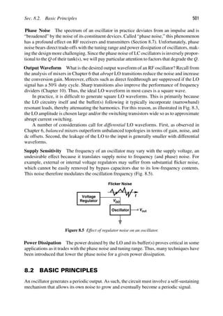
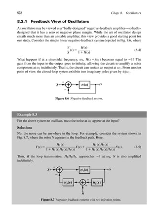
![Sec. 8.2. Basic Principles 503
The above example leads to a general and powerful analytical point: in the small-signal
model of an oscillator, the impedance seen between any two nodes (one of which is not
ground) in the signal path goes to infinity at the oscillation frequency, ω1, because a noise
current at ω1 injected between these two nodes produces an infinitely large swing. This
observation can be used to determine the oscillation condition and frequency.
Example 8.4
Derive an expression for Y/X in Fig. 8.6 in the vicinity of ω 5 ω1 if H( jω1) 5 21.
Solution:
If ω 5 ω1 1 ω, we can approximate H( jω) by the first two terms in its Taylor series:
H[j(ω1 1 ω)] ≈ H( jω1) 1 ω
dH( jω1)
dω
. (8.6)
Since H( jω1) 5 21, we have
Y
X
[j(ω1 1 ω)] 5
H( jω1) 1 ω
dH( jω1)
dω
ω
dH( jω1)
dω
(8.7)
≈
H( jω1)
ω
dH( jω1)
dω
(8.8)
≈
21
ω
dH( jω1)
dω
. (8.9)
As expected, Y/X → ∞ as ω → 0, with a “sharpness” proportional to dH/dω.
Since H(s) is a complex function, the condition H( jω1) 5 21 can equivalently be
expressed as
|H(s 5 jω1)| 5 1 (8.10)
∠H(s 5 jω1) 5 1808
, (8.11)
which are called “Barkhausen’s criteria” for oscillation. Let us examine these two condi-
tions to develop more insight. We recognize that a signal at ω1 experiences a gain of unity
and a phase shift of 1808 as it travels through H(s) [Fig. 8.8(a)]. Bearing in mind that the
system is originally designed to have negative feedback (as denoted by the input subtrac-
tor), we conclude that the signal at ω1 experiences a total phase shift of 3608 [Fig. 8.8(b)]
as it travels around the loop. This is, of course, to be expected: for the circuit to reach
steady state, the signal returning to A must exactly coincide with the signal that started at A.](https://image.slidesharecdn.com/rfmicroelectronicsrazavi-230814101614-71259b59/85/RF-MICROELECTRONICS_Razavi-pdf-528-320.jpg)
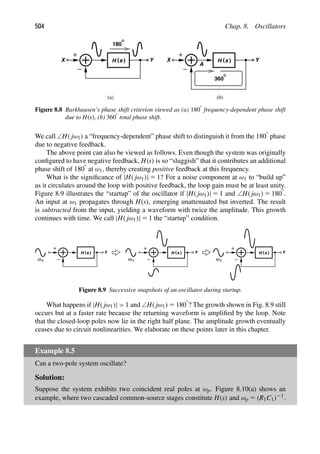
![Sec. 8.2. Basic Principles 505
Example 8.5 (Continued)
This system cannot satisfy both of Barkhausen’s criteria because the phase shift associated
with each stage reaches 908 only at ω 5 ∞, but |H(∞)| 5 0. Figure 8.10(b) plots |H| and
∠H as a function of frequency, revealing no frequency at which both conditions are met.
Thus, the circuit cannot oscillate.
R
C1
R
VDD
C1
1 1
X
Y
ω
( )
ω
H
0
ω
0
( )
ω
H
−180
−90
(log scale)
(log scale)
(log scale)
C
1
R1 1
Z
X Y
ω
( )
ω
H
0
ω
0
( )
ω
H
−180
(log scale)
(log scale)
(log scale)
(a) (b)
(c (
) d)
ω1
Figure 8.10 (a) Two CS stages in feedback, (b) loop transmission response, (c) two integrators in
feedback, (d) loop transmission response.
But, what if both poles are located at the origin? Realized as two ideal integrators in a
loop [Fig. 8.10(c)], such a circuit does oscillate because each integrator contributes a phase
shift of 2908 at any nonzero frequency. Shown in Fig. 8.10(d) are |H| and ∠H for this
system.
Our study thus far allows us to predict the frequency of oscillation: we seek the
frequency at which the total phase shift around the loop is 3608 and determine whether
the loop gain reaches unity at this frequency. (An exception is described in the example
below.) This calculation, however, does not predict the oscillation amplitude. In a perfectly](https://image.slidesharecdn.com/rfmicroelectronicsrazavi-230814101614-71259b59/85/RF-MICROELECTRONICS_Razavi-pdf-530-320.jpg)
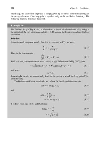
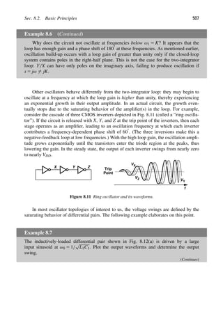
![508 Chap. 8. Oscillators
Example 8.7 (Continued)
V
M
I SS
out
R Rp
p
VDD
L1 L1 C1
C1
M 1 2
in
V
t
I
I
(b)
D1
D2
I SS
(a)
t
A
+
A
−
A
4
π
+
A
4
π
−
(c)
0 f
A
π
2
f0
+
A
π
2
f0
−
Figure 8.12 (a) Differential pair with tank loads, (b) drain currents, (c) first harmonic of a square
wave.
Solution:
With large input swings, M1 and M2 experience complete switching in a short transition
time, injecting nearly square current waveforms into the tanks [Fig. 8.12(b)]. Each drain
current waveform has an average of ISS/2 and a peak amplitude of ISS/2. The first har-
monic of the current is multiplied by Rp, whereas higher harmonics are attenuated by the
tank selectivity. Recall from the Fourier expansion of a square wave of peak amplitude A
(with 50% duty cycle) that the first harmonic exhibits a peak amplitude of (4/π)A (slightly
greater than A) [Fig. 8.12(c)]. The peak single-ended output swing is therefore equal to
(4/π)(ISS/2)Rp 5 2ISSRp/π, yielding a peak differential output swing of
Vout 5
4
π
ISSRp. (8.21)
If interested in carrying out this calculation in the frequency domain, the reader is cau-
tioned that the spectrum of the first harmonic contains two impulses, each having an area
of (2/π)A [not (4/π)A] [Fig. 8.12(c)].
8.2.2 One-Port View of Oscillators
In the previous section, we considered oscillators as negative-feedback systems that expe-
rience sufficient positive feedback at some frequency. An alternative perspective views](https://image.slidesharecdn.com/rfmicroelectronicsrazavi-230814101614-71259b59/85/RF-MICROELECTRONICS_Razavi-pdf-533-320.jpg)
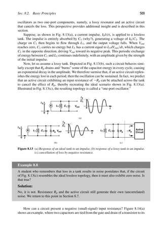
![510 Chap. 8. Oscillators
V
X
I
X
Z
gm
−
C1C2ω2
C1C2
+
C1 2
C
(a) (b)
C
M 1
2
C1
Z
in
in
I X
−
Figure 8.14 (a) Circuit providing negative resistance, (b) equivalent circuit.
source. The impedance Zin can be obtained by noting that C1 carries a current equal to 2IX,
generating a gate-source voltage of 2IX/(C1s) and hence a drain current of 2IXgm/(C1s).
The difference between IX and the drain current flows through C2, producing a voltage
equal to [IX 1 IXgm/(C1s)]/(C2s). This voltage must be equal to VGS 1 VX:
2
IX
C1s
1 VX 5
IX 1 IX
gm
C1s
1
C2s
. (8.22)
It follows that
VX
IX
(s) 5
1
C1s
1
1
C2s
1
gm
C1C2s2
. (8.23)
For a sinusoidal input, s 5 jω,
VX
IX
( jω) 5
1
jC1ω
1
1
jC2ω
2
gm
C1C2ω2
. (8.24)
Thus, the input impedance can be viewed as a series combination of C1, C2, and a negative
resistance equal to 2gm/(C1C2ω2) [Fig. 8.14(b)]. Interestingly, the negative resistance
varies with frequency.
Having found a negative resistance, we can now attach it to a lossy tank so as to con-
struct an oscillator. Since the capacitive component in Eq. (8.24) can become part of the
tank, we simply connect an inductor to the negative-resistance port (Fig. 8.15), seeking the
condition for oscillation. In this case, it is simpler to model the loss of the inductor by a
series resistance, RS. The circuit oscillates if
RS 5
gm
C1C2ω2
. (8.25)
Under this condition, the circuit reduces to L1 and the series combination of C1 and C2,
exhibiting an oscillation frequency of
ωosc 5
1
L1
C1C2
C1 1 C2
. (8.26)](https://image.slidesharecdn.com/rfmicroelectronicsrazavi-230814101614-71259b59/85/RF-MICROELECTRONICS_Razavi-pdf-535-320.jpg)
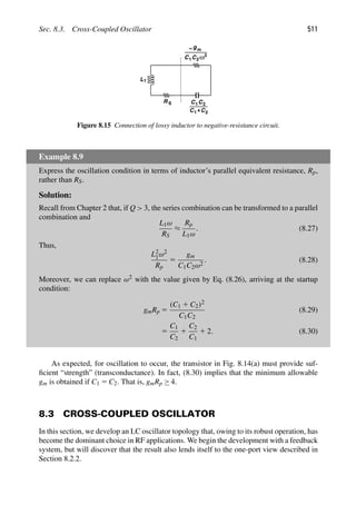
![512 Chap. 8. Oscillators
Vout
Rp
VDD
L1
C1
M 1
in
V
ω
0
ω
0
−180
−90
Vout
in
V
ω0
Vout
in
V
−270
(a) (b)
Figure 8.16 (a) Tuned amplifier, (b) frequency response.
We wish to build a negative-feedback oscillatory system using “LC-tuned” amplifier
stages. Figure 8.16(a) shows such a stage, where C1 denotes the total capacitance seen
at the output node and Rp the equivalent parallel resistance of the tank at the resonance
frequency. We neglect CGD here but will see that it can be readily included in the final
oscillator topology.
Let us examine the frequency response of the stage. At very low frequencies, L1
dominates the load and
Vout
Vin
≈ 2 gmL1s. (8.31)
That is, |Vout/Vin| is very small and ∠(Vout/Vin) remains around 2908 [Fig. 8.16(b)]. At
the resonance frequency, ω0, the tank reduces to Rp and
Vout
Vin
5 2 gmRp. (8.32)
The phase shift from the input to the output is thus equal to 21808. At very high
frequencies, C1 dominates, yielding
Vout
Vin
≈ 2 gm
1
C1s
. (8.33)
Thus, |Vout/Vin| diminishes and ∠(Vout/Vin) approaches 1 908 ( 5 22708).
Can the circuit of Fig. 8.16(a) oscillate if its input and output are shorted? As evidenced
by the open-loop magnitude and phase plots shown in Fig. 8.16(b), no frequency satisfies
Barkhausen’s criteria; the total phase shift fails to reach 3608 at any frequency.
Upon closer examination, we recognize that the circuit provides a phase shift of 1808
with possibly adequate gain (gmRp) at ω0. We simply need to increase the phase shift to
3608, perhaps by inserting another stage in the loop. Illustrated in Fig. 8.17(a), the idea is to
cascade two identical LC-tuned stages so that, at resonance, the total phase shift around the](https://image.slidesharecdn.com/rfmicroelectronicsrazavi-230814101614-71259b59/85/RF-MICROELECTRONICS_Razavi-pdf-537-320.jpg)
![Sec. 8.3. Cross-Coupled Oscillator 513
Rp
VDD
L1
C1
M
Rp
L1
C1
M 1 2
Y
X
t
VDD
VX
VY
(a) (b)
Figure 8.17 Cascade of two tuned amplifiers in feedback loop.
loop is equal to 3608. The circuit oscillates if the loop gain is equal to or greater than unity:
gmRp
2
≥ 1. (8.34)
Example 8.10
Assuming that the circuit of Fig. 8.17(a) oscillates, plot the voltage waveforms at X and Y.
Solution:
At t 5 0, VX 5 VY 5 VDD. As a noise component at ω0 is amplified and circulated around
the loop, VX and VY begin to grow while maintaining a 1808 phase difference [Fig. 8.17(b)].
A unique attribute of inductive loads is that they can provide peak voltages above the
supply.1
The growth of VX and VY ceases when M1 and M2 enter the triode region for part
of the period, reducing the loop gain.
The above circuit can be redrawn as shown in Fig. 8.18(a) and is called a “cross-
coupled” oscillator due to the connection of M1 and M2. Forming the core of most RF
L R C
M
VDD
RP
L
C
M 1 2
X Y
1
1 1 1
L R C
M
VDD
RP
L
C
M 1 2
X Y
1
1
1
1
I SS
(a) (b) (c)
p
p
Figure 8.18 (a) Simple cross-coupled oscillator, (b) addition of tail current, (c) equivalence to a
differential pair placed in feedback.
1. If L1 has no series resistance, then its average voltage drop must be zero; thus, VX and VY must go above
VDD and below VDD.](https://image.slidesharecdn.com/rfmicroelectronicsrazavi-230814101614-71259b59/85/RF-MICROELECTRONICS_Razavi-pdf-538-320.jpg)
![514 Chap. 8. Oscillators
oscillators used in practice, this topology entails many interesting properties and will be
studied from different perspectives in this chapter.
Let us compute the oscillation frequency of the circuit. The capacitance at X includes
CGS2, CDB1, and the effect of CGD1 and CGD2. We note that (a) CGD1 and CGD2 are in
parallel, and (b) the total voltage change across CGD1 1 CGD2 is equal to twice the voltage
change at X (or Y) because VX and VY vary differentially. Thus,
ωosc 5
1
√
L1(CGS2 1 CDB1 1 4CGD 1 C1)
. (8.35)
Here, C1 denotes the parasitic capacitance of L1 plus the input capacitance of the next stage.
The oscillator of Fig. 8.18(a) suffers from poorly-defined bias currents. Since the aver-
age VGS of each transistor is equal to VDD, the currents strongly depend on the mobility,
threshold voltage, and temperature. With differential VX and VY, we surmise that M1 and
M2 can operate as a differential pair if they are tied to a tail current source. Shown in
Fig. 8.18(b), the resulting circuit is more robust and can be viewed as an inductively-loaded
differential pair with positive feedback [Fig. 8.18(c)]. The oscillation amplitude grows
until the pair experiences saturation. We sometimes refer to this circuit as the “tail-biased
oscillator” to distinguish it from other cross-coupled topologies.
Example 8.11
Compute the voltage swings in the circuit of Fig. 8.18(b) if M1 and M2 experience complete
current switching with abrupt edges.
Solution:
From Example 8.7, the drain current of each transistor swings between zero and ISS,
yielding a peak differential output swing of
VXY ≈
4
π
ISSRp. (8.36)
The above-supply swings in the cross-coupled oscillator of Fig. 8.18(b) raise concern
with respect to transistor reliability. The instantaneous voltage difference between any two
terminals of M1 or M2 must remain below the maximum value allowed by the technology.
Figure 8.19 shows a “snapshot” of the circuit when M1 is off and M2 is on. Each transistor
may experience stress under the following conditions: (1) The drain reaches VDD 1 Va,
where Va is the peak single-ended swing, e.g., (2/π)ISSRp, while the gate drops to VDD 2
Va. The transistor remains off, but its drain-gate voltage is equal to 2Va and its drain-source
voltage is greater than 2Va (why?). (2) The drain falls to VDD 2 Va while the gate rises to
VDD 1 Va. Thus, the gate-drain voltage reaches 2Va and the gate-source voltage exceeds
2Va. We note that both VDS1 and VGS2 may assume excessively large values. Proper choice
of Va, ISS, and device dimensions avoids stressing the transistors.
The reader may wonder how the inductance value and the device dimensions are
selected in the cross-coupled oscillator. We defer the design procedure to after we have
studied voltage-controlled oscillators and phase noise (Section 8.8).](https://image.slidesharecdn.com/rfmicroelectronicsrazavi-230814101614-71259b59/85/RF-MICROELECTRONICS_Razavi-pdf-539-320.jpg)
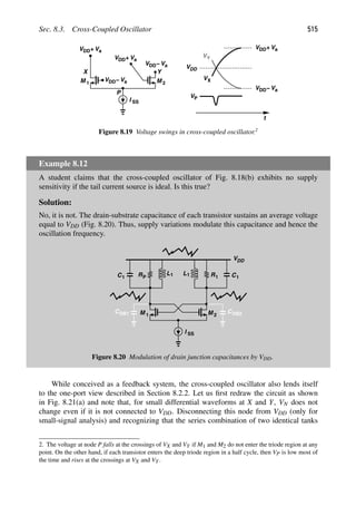
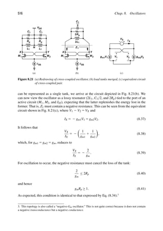
![Sec. 8.4. Three-Point Oscillators 517
Choice of gm The foregoing studies may suggest that the gm of the cross-coupled
transistors in Fig. 8.18(b) can be chosen slightly greater than Rp of the tank to ensure oscil-
lation. However, this choice leads to small voltage swings; if the swings are large, e.g., if
M1 and M2 switch completely, then the gm falls below 1/Rp for part of the period, failing to
sustain oscillation. (That is, with gm ≈ 1/Rp, M1 and M2 must remain linear to avoid com-
pression.) In practice, therefore, we design the circuit for nearly complete current steering
between M1 and M2, inevitably choosing a gm quite higher than 1/Rp.
8.4 THREE-POINT OSCILLATORS
As observed in Section 8.2.2, the circuit of Fig. 8.14(a) can be attached to an inductor so
as to form an oscillator. Note that the derivation of the impedance Zin does not assume
any terminal is grounded. Thus, three different oscillator topologies can be obtained by
grounding each of the transistor terminals. Figures 8.22(a), (b), and (c) depict the resulting
circuits if the source, the gate, or the drain is (ac) grounded, respectively. In each case, a
current source defines the bias current of the transistor. [The gate of M1 in Fig. 8.22(b) and
the left terminal of L1 in Fig. 8.22(c) must be tied to a proper potential, e.g., Vb 2 VDD.]
M 1 C
C
L1
M 1
L1
2
1
C1 C2
M 1 C2
C1
L1
(c)
(a) (b)
VDD
Vb
Vb
Figure 8.22 Variants of three-point oscillator, (a) with source grounded, (b) with gate grounded
(Colpitts oscillator), (c) with drain grounded (Clapp oscillator).
It is important to bear in mind that the operation frequency and startup condition of all
three oscillators in Fig. 8.22 are given by Eqs. (8.26) and (8.30), respectively. Specifically,
the transistor must provide sufficient transconductance to satisfy
gmRp ≥ 4 (8.42)
if C1 5 C2. This condition is more stringent than Eq. (8.34) for the cross-coupled oscillator,
suggesting that the circuits of Fig. 8.22 may fail to oscillate if the inductor Q is not very
high. This is the principal disadvantage of these oscillators and the reason for their lack of
popularity.
Another drawback of the circuits shown in Fig. 8.22 is that they produce only single-
ended outputs. It is possible to couple two copies of one oscillator so that they operate
differentially. Shown in Fig. 8.23 is an example, where two instances of the oscillator
in Fig. 8.22(c) are coupled at node P. Resistor R1 establishes a dc level equal to VDD
at P and at the gates of M1 and M2. More importantly, if chosen properly, this resistor](https://image.slidesharecdn.com/rfmicroelectronicsrazavi-230814101614-71259b59/85/RF-MICROELECTRONICS_Razavi-pdf-542-320.jpg)
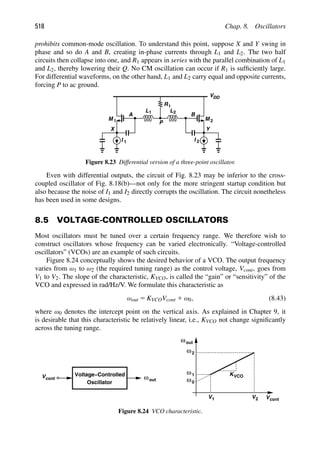
![Sec. 8.5. Voltage-Controlled Oscillators 519
Example 8.13
As explained in Example 8.12, the cross-coupled oscillator exhibits sensitivity to VDD.
Considering VDD as the “control voltage,” determine the gain.
Solution:
We have
ωosc 5
1
√
L1(C1 1 CDB)
, (8.44)
where C1 includes all circuit capacitances except CDB. Thus,
KVCO 5
∂ωout
∂VDD
(8.45)
5
∂ωosc
∂CDB
·
∂CDB
∂VDD
. (8.46)
The junction capacitance, CDB, is approximated as
CDB 5
CDB0
1 1
VDD
φB
m , (8.47)
where φB denotes the junction’s built-in potential and m is around 0.3 to 0.4. It follows
from Eqs. (8.46) and (8.47) that
KVCO 5
21
2
√
L1
·
1
√
C1 1 CDB(C1 1 CDB)
·
2mCDB0
φB
1 1
VDD
φB
m 1 1
(8.48)
5
CDB
C1 1 CDB
·
m
2φB 1 2VDD
ωosc. (8.49)
In order to vary the frequency of an LC oscillator, the resonance frequency of its tank(s)
must be varied. Since it is difficult to vary the inductance electronically, we only vary the
capacitance by means of a varactor. As explained in Chapter 7, MOS varactors are more
commonly used than pn junctions, especially in low-voltage design. We thus construct
our first VCO as shown in Fig. 8.25(a), where varactors MV1 and MV2 appear in parallel
with the tanks (if Vcont is provided by an ideal voltage source). Note that the gates of the
varactors are tied to the oscillator nodes and the source/drain/n-well terminals to Vcont. This
avoids loading X and Y with the capacitance between the n-well and the substrate.
Since the gates of MV1 and MV2 reside at an average level equal to VDD, their gate-
source voltage remains positive and their capacitance decreases as Vcont goes from zero to
VDD [Fig. 8.25(b)]. This behavior persists even in the presence of large voltage swings at
X and Y and hence across MV1 and MV2. The key point here is that the average voltage](https://image.slidesharecdn.com/rfmicroelectronicsrazavi-230814101614-71259b59/85/RF-MICROELECTRONICS_Razavi-pdf-544-320.jpg)
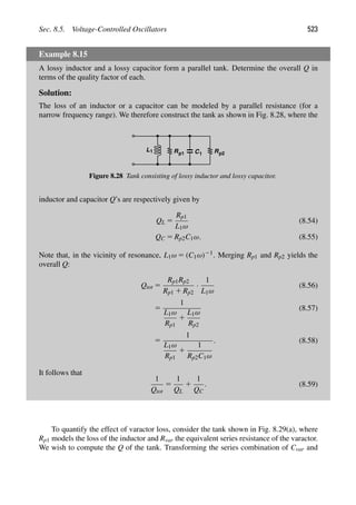
![524 Chap. 8. Oscillators
L R C
1 1
p1
Cvar
Rvar
L R C
1 1
p1 Rp2 Cvar
(a) (b)
Figure 8.29 (a) Tank using lossy varactor, (b) equivalent circuit.
Rvar to a parallel combination [Fig. 8.29(b)], we have from Chapter 2
Rp2 5
1
C2
varω2Rvar
. (8.60)
To utilize our previous results, we combine C1 and Cvar. The Q associated with C1 1 Cvar
is equal to
QC 5 RP2(C1 1 Cvar)ω (8.61)
5
C1 1 Cvar
C2
varωRvar
. (8.62)
Recognizing that Qvar 5 (CvarωRvar)21, we have
QC 5
1 1
C1
Cvar
Qvar. (8.63)
In other words, the Q of the varactor is “boosted” by a factor of 1 1 C1/Cvar. The overall
tank Q is therefore given by
1
Qtot
5
1
QL
1
1
1 1
C1
Cvar
Qvar
. (8.64)
For frequencies as high as several tens of gigahertz, the first term in Eq. (8.64) is dominant
(unless a long channel is chosen for the varactors).
Equation (8.64) can be generalized if the tank consists of an ideal capacitor, C1, and
lossy capacitors, C2-Cn, that exhibit a series resistance of R2-Rn, respectively. The reader
can prove that
1
Qtot
5
1
QL
1
C2
Ctot
1
Q2
1 · · · 1
Cn
Ctot
1
Qn
, (8.65)
where Ctot 5 C1 1 · · · 1 Cn and Qj 5 (RjCjω)21.
8.6 LC VCOs WITH WIDE TUNING RANGE
8.6.1 VCOs with Continuous Tuning
The tuning range obtained from the C–V characteristic depicted in Fig. 8.27 may prove
prohibitively narrow, particularly because the capacitance range corresponding to negative](https://image.slidesharecdn.com/rfmicroelectronicsrazavi-230814101614-71259b59/85/RF-MICROELECTRONICS_Razavi-pdf-549-320.jpg)
![Sec. 8.6. LC VCOs with Wide Tuning Range 525
VGS (for Vcont VDD) remains unused. We must therefore seek oscillator topologies that
allow both positive and negative (average) voltages across the varactors, utilizing almost
the entire range from Cmin to Cmax.
Figure 8.30(a) shows one such topology. Unlike the tail-biased configuration studied in
Section 8.3, this circuit defines the bias currents of M1 and M2 by a top current source, IDD.
We analyze this circuit by first computing the output common-mode level. In the absence
of oscillation, the circuit reduces to that shown in Fig. 8.30(b), where M1 and M2 share IDD
equally and are configured as diode-connected devices. Thus, the CM level is simply given
by the gate-source voltage of a diode-connected transistor carrying a current of IDD/2.4
For
example, for square-law devices,
VGS1,2 5
IDD
μnCox(W/L)
1 VTH. (8.66)
L
M
L
M 1 2
1 1
I
Y
X
M v1 M v2
Vcont
Cvar
C
0 Vcont
(a) (b)
VDD
DD
P
M
M 1 2
I
VDD
DD
V
2
DD VDD
max
Cvar1
Cmin
V1 V
Cvar2
2
(c)
Figure 8.30 (a) Top-biased VCO, (b) equivalent circuit for CM calculation, (c) varactor range used.
We select the transistor dimensions such that the CM level is approximately equal
to VDD/2. Consequently, as Vcont varies from 0 to VDD, the gate-source voltage of the
varactors, VGS,var, goes from 1 VDD/2 to 2VDD/2, sweeping almost the entire capacitance
range from Cmin to Cmax [Fig. 8.30(c)]. In practice, the circuit producing Vcont (the charge
pump) can handle only the voltage range from V1 to V2, yielding a capacitance range from
Cvar1 to Cvar2.
The startup condition, oscillation frequency, and output swing of the oscillator shown
in Fig. 8.30(a) are similar to those derived for the tail-biased circuit of Fig. 8.18(b). Also,
L1 and L2 are realized as a single symmetric inductor so as to achieve a higher Q; the center
tap of the inductor is tied to IDD.
While providing a wider range than its tail-biased counterpart, the topology of
Fig. 8.30(a) suffers from a higher phase noise. As studied in Section 8.7, this penalty arises
primarily from the modulation of the output CM level (and hence the varactors) by the
noise current of IDD, as evidenced by Eq. (8.66). This effect does not occur in the tail-
biased oscillator because the output CM level is “pinned” at VDD by the low dc resistance
of the inductors. The following example illustrates this difference.
4. With large-signal oscillation, the nonlinearity of M1 and M2 shifts the output CM level slightly, but we
neglect this effect here.](https://image.slidesharecdn.com/rfmicroelectronicsrazavi-230814101614-71259b59/85/RF-MICROELECTRONICS_Razavi-pdf-550-320.jpg)
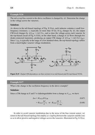
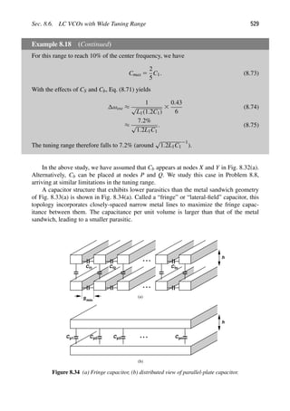
![530 Chap. 8. Oscillators
Example 8.19
Explain why the fringe structure provides a larger capacitance per unit volume.
Solution:
Suppose a two-layer metal sandwich capacitor is viewed as the sum of small units
[Fig. 8.34(b)]. Given by the vertical spacing, h, the capacitance between the two plates
is equal to Cp1 1 · · · 1 Cpn. Now, we decompose each plate into a number of narrow
lines, with a spacing equal to the minimum allowed by the technology, Smin [Fig. 8.34(a)].
For example, Smin 5 0.15 μm whereas h 5 0.5 μm. We now recognize that some of the
parallel-plate capacitances, Cpj, are omitted, but about twice as many fringe capacitors,
Cfj, have been added. Also, since Smin h, Cfj Cpj. Thus, the overall capacitance rises
substantially.
Three other issues in Fig. 8.32(a) merit consideration. First, since R1 and R2 appear
approximately in parallel with the tanks, their value must be chosen much greater than Rp.
(Even a tenfold ratio proves inadequate as it lowers the Q by about 10%.) Second, noise on
the mid-supply bias, Vb, directly modulates the varactors and must therefore be minimized.
Third, as studied in the transceiver design example of Chapter 13, the noise of R1 and R2
modulates the varactors, producing substantial phase noise.
Another VCO topology that naturally provides an output CM level approximately equal
to VDD/2 is shown in Fig. 8.35. The circuit can be viewed as two back-to-back CMOS
inverters, except that the sources of the NMOS devices are tied to a tail current, or as a
cross-coupled NMOS pair and a cross-coupled PMOS pair sharing the same bias current.
Proper choice of device dimensions and ISS can yield a CM level at X and Y around VDD/2,
thereby maximizing the tuning range.
M
M
Y
X
M v1 M v2
Vcont
VDD
I SS
M
M
1 2
3 4
LXY
Figure 8.35 VCO using NMOS and PMOS cross-coupled pairs.
In this circuit, the bias current is “reused” by the PMOS devices, providing a higher
transconductance. But a more important advantage of the above topology over those in
Figs. 8.25(a), 8.30(a), and 8.32(a) is that it produces twice the voltage swing for a given bias
current and inductor design. To understand this point, we assume LXY in the complementary
topology is equal to L1 1 L2 in the previous circuits. Thus, LXY presents an equivalent
parallel resistance of 2Rp. Drawing the circuit for each half cycle as shown in Fig. 8.36, we](https://image.slidesharecdn.com/rfmicroelectronicsrazavi-230814101614-71259b59/85/RF-MICROELECTRONICS_Razavi-pdf-555-320.jpg)
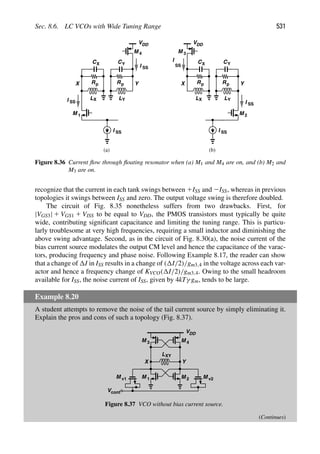
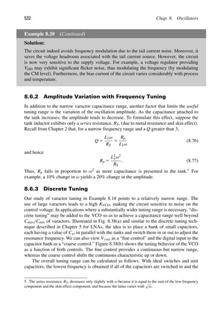
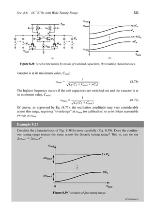
![534 Chap. 8. Oscillators
Example 8.21 (Continued)
Solution:
We expect ωosc1 to be greater than ωosc2 because, with nCu switched into the tanks, the
varactor sees a larger constant capacitance. In fact, from Eq. (8.53), we have
ωosc1 ≈
1
√
L1C1
Cmax 2 Cmin
2C1
, (8.80)
and
ωosc2 ≈
1
√
L1(C1 1 nCu)
Cmax 2 Cmin
2(C1 1 nCu)
. (8.81)
It follows that
ωosc1
ωosc2
5
1 1
nCu
C1
3/2
. (8.82)
This variation in KVCO proves undesirable in PLL design.
The discrete tuning technique shown in Fig. 8.38(a) entails several difficult issues.
First, the on-resistance, Ron, of the switches that control the unit capacitors degrades the
Q of the tank. Applying Eq. (8.65) to the parallel combination shown in Fig. 8.40 and
denoting [(Ron/n)(nCu)ω]21 by Qbank, we have
1
Qtot
5
1
QL
1
Cvar
C1 1 Cvar 1 nCu
1
Qvar
1
nCu
C1 1 Cvar 1 nCu
1
Qbank
(8.83)
5
RS
L1ω
1
Cvar
C1 1 Cvar 1 nCu
RvarCvarω 1
nCu
C1 1 Cvar 1 nCu
RonCuω. (8.84)
Cu
n
R
n
on
R
C1
C
Rvar
var
S
Capacitor
Bank
L1
Figure 8.40 Equivalent circuit for Q calculation.
Can we simply increase the width of the switch transistors in Fig. 8.38(a) so as to min-
imize the effect of Ron? Unfortunately, wider switches introduce a larger capacitance from
the bottom plate of the unit capacitors to ground, thereby presenting a substantial capaci-
tance to the tanks when the switches are off. As shown in Fig. 8.41, each branch in the bank
contributes a capacitance of CGD 1 CDB to the tank if Cu CGD 1 CDB. For n branches,
therefore, C1 incurs an additional constant component equal to n(CGD 1 CDB), further](https://image.slidesharecdn.com/rfmicroelectronicsrazavi-230814101614-71259b59/85/RF-MICROELECTRONICS_Razavi-pdf-559-320.jpg)
![Sec. 8.6. LC VCOs with Wide Tuning Range 535
VDD
L1
C1
CGD+ CDB
Cu
Discrete
Tuning Circuit
Figure 8.41 Effect of switch parasitic capacitances.
limiting the fine tuning range. For example, ωosc1 in Eq. (8.80) must be rewritten as
ωosc1 ≈
1
√
L1(C1 1 nCGD 1 nCDB)
Cmax 2 Cmin
2(C1 1 nCGD 1 nCDB)
. (8.85)
This trade-off between the Q and the tuning range limits the use of discrete tuning.
The problem of switch on-resistance can be alleviated by exploiting the differential
operation of the oscillator. Illustrated in Fig. 8.42(a), the idea is to place the main switch,
S1, between nodes A and B so that, with differential swings at these nodes, only half of Ron1
appears in series with each unit capacitor [Fig. 8.42(b)]. This allows a twofold reduction
in the switch width for a given resistance. Switches S2 and S3 are minimum-size devices,
merely defining the CM level of A and B.
L
M
L
M 1 2
1 1
VDD
I SS
Y
X
Cu
Cu
1
S
S2 S3
Band
Control
Y
X
Cu
Cu
Ron2 Ron3
R
2
on1
R
2
on1
(a) (b)
A B B
A
Figure 8.42 (a) Use of floating switch, (b) equivalent circuit.
The second issue in discrete tuning relates to potential “blind” zones. Suppose, as
shown in Fig. 8.43(a), unit capacitor number j is switched out, creating a frequency change
equal to ω4 2 ω2 ≈ ω3 2 ω1, but the fine tuning range provided by the varactor, ω4 2 ω3, is
less than ω4 2 ω2. Then, the oscillator fails to cover the range between ω2 and ω3 for any
combination of fine and coarse controls.](https://image.slidesharecdn.com/rfmicroelectronicsrazavi-230814101614-71259b59/85/RF-MICROELECTRONICS_Razavi-pdf-560-320.jpg)
![536 Chap. 8. Oscillators
(a) (b)
0 Vcont
ωout
ω
Cu
n
Cu
)
−1
) j
1
ω2
0 Vcont
ωout
ω
Cu
n
Cu
)
−1
) j
1
ω
ω3
3
ω2
ω4
Blind
Zone
ω4
Figure 8.43 (a) Blind zone in discrete tuning, (b) overlap between consecutive characteristics to
avoid blind zone.
To avoid blind zones, each two consecutive tuning characteristics must have some
overlap. Depicted in Fig. 8.43(b), this precaution translates to smaller unit capacitors but
a larger number of them and hence a complex layout. As explained in Chapter 13, the
unit capacitors can be chosen unequal to mitigate this issue. Note that the overlap is also
necessary to avoid excessive variation of KVCO near the ends of each tuning curve. For
example, around ω2 in Fig. 8.43(b), the lower tuning curve flattens out, requiring that the
upper one be used.
Some recent designs have employed oscillators with only discrete tuning. Called
“digitally-controlled oscillators” (DCOs), such circuits must employ very fine frequency
stops. Examples are described in [2].
In Chapter 13, we design and simulate a VCO with continuous and discrete tuning for
11a/g applications.
8.7 PHASE NOISE
The design of VCOs must deal with trade-offs among tuning range, phase noise, and power
dissipation. Our study has thus far focused on the task of tuning. We now turn our attention
to phase noise.
8.7.1 Basic Concepts
An ideal oscillator produces a perfectly-periodic output of the form x(t) 5 A cos ωct. The
zero crossings occur at exact integer multiples of Tc 5 2π/ωc. In reality, however, the
noise of the oscillator devices randomly perturbs the zero crossings. To model this pertur-
bation, we write x(t) 5 A cos[ωct 1 φn(t)], where φn(t) is a small random phase quantity
that deviates the zero crossings from integer multiples of Tc. Figure 8.44 illustrates the two
waveforms in the time domain. The term φn(t) is called the “phase noise.”
The waveforms in Fig. 8.44 can also be viewed from another, slightly different,
perspective. We can say that the period remains constant if x(t) 5 A cos ωct but varies
randomly if x(t) 5 A cos[ωct 1 φn(t)] (as indicated by T1, . . . , Tm in Fig. 8.44). In other](https://image.slidesharecdn.com/rfmicroelectronicsrazavi-230814101614-71259b59/85/RF-MICROELECTRONICS_Razavi-pdf-561-320.jpg)
![Sec. 8.7. Phase Noise 537
t
t
t
cosωc
A
t
ωc
A cos [ + φ (t
n )]
T1 T2 Tm
Figure 8.44 Output waveforms of an ideal and a noisy oscillator.
words, the frequency of the waveform is constant in the former case but varies ran-
domly in the latter. This observation leads to the spectrum of the oscillator output. For
x(t) 5 A cos ωct, the spectrum consists of a single impulse at ωc [Fig. 8.45(a)], whereas for
x(t) 5 A cos[ωct 1 φn(t)] the frequency experiences random variations, i.e., it departs from
ωc occasionally. As a consequence, the impulse is “broadened” to represent this random
departure [Fig. 8.45(b)].
ω
ωc ω
ωc
Sout Sout
(a) (b)
Figure 8.45 Output spectra of (a) an ideal, and (b) a noisy oscillator.
Example 8.22
Explain why the broadened impulse cannot assume the shape shown in Fig. 8.46.
ω
ωc
Sout
ωc+ Δω
ωc Δω
−
Figure 8.46 Flat spectrum around oscillation frequency.
(Continues)](https://image.slidesharecdn.com/rfmicroelectronicsrazavi-230814101614-71259b59/85/RF-MICROELECTRONICS_Razavi-pdf-562-320.jpg)
![538 Chap. 8. Oscillators
Example 8.22 (Continued)
Solution:
This spectrum occurs if the oscillator frequency has equal probability of appearing any-
where between ωc 2 ω and ωc 1 ω. However, we intuitively expect that the oscillator
prefers ωc to other frequencies, thus spending lesser time at frequencies that are farther
from ωc. This explains the declining phase noise “skirts” in Fig. 8.45(b).
Our focus on noise in the zero crossings rather than noise on the amplitude arises
from the assumption that the latter is removed by hard switching in stages following the
oscillator. For example, the switching transistors in an active mixer spend little time near
equilibrium, “masking” most of the LO amplitude noise for the rest of the time.
The spectrum of Fig. 8.45(b) can be related to the time-domain expression. Since
φn(t) 1 rad,
x(t) 5 A cos[ωct 1 φn(t)] (8.86)
≈ A cos ωct 2 A sin ωct sin[φn(t)] (8.87)
≈ A cos ωct 2 Aφn(t) sin ωct. (8.88)
That is, the spectrum of x(t) consists of an impulse at ωc and the spectrum of φn(t) trans-
lated to a center frequency of ωc. Thus, the declining skirts in Fig. 8.45(b) in fact represent
the behavior of φn(t) in the frequency domain.
In phase noise calculations, many factors of 2 or 4 appear at different stages and must
be carefully taken into account. For example, as illustrated in Fig. 8.47, (1) since φn(t)
in Eq. (8.88) is multiplied by sin ωct, its power spectral density, Sφn, is multiplied by 1/4
as it is translated to ±ωc; (2) A spectrum analyzer measuring the resulting spectrum folds
the negative-frequency spectrum atop the positive-frequency spectrum, raising the spectral
density by a factor of 2.
How is the phase noise quantified? Since the phase noise falls at frequencies farther
from ωc, it must be specified at a certain “frequency offset,” i.e., a certain difference with
ω
0
η
φ (t
n t
sinω
) c
ω
ω
0
+
ω
−
η
4
c
c
Spectrum of
RF Waveform
Spectrum
Analyzer
ω
Measured
Spectrum
ωc
η
2
S ( )
ω
φn
Figure 8.47 Various factors of 4 and 2 that arise in conversion of noise to phase noise.](https://image.slidesharecdn.com/rfmicroelectronicsrazavi-230814101614-71259b59/85/RF-MICROELECTRONICS_Razavi-pdf-563-320.jpg)
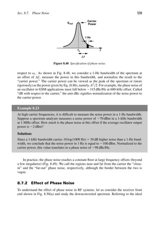
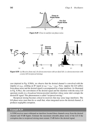
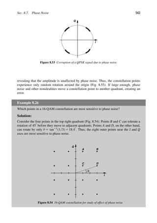
![544 Chap. 8. Oscillators
8.7.3 Analysis of Phase Noise: Approach I
Oscillator phase noise has been under study for decades [3]–[17], leading to a multitude of
analysis techniques in the frequency and time domains. The calculation of phase noise by
hand still remains tedious, but simulation tools such as Cadence’s SpectreRF have greatly
simplified the task. Nonetheless, a solid understanding of the mechanisms that give rise to
phase noise proves essential to oscillator design. In this section, we analyze these mecha-
nisms. In particular, we must answer two important questions: (1) how much and at what
point in an oscillation cycle does each device “inject” noise? (2) how does the injected
noise produce phase noise in the output voltage waveform?
Q of an Oscillator In Chapters 2 and 7, we derived various expressions for the Q of an LC
tank. We know intuitively that a high Q signifies a sharper resonance, i.e., a higher selec-
tivity. Another definition of the Q that is especially well-suited to oscillators is illustrated in
Fig. 8.55. Here, the circuit is viewed as a feedback system and the phase of the open-loop
transfer function, φ(ω), is examined at the resonance frequency, ω0. The “open-loop” Q is
defined as
Q 5
ω0
2
|
dφ
dω
|. (8.95)
This definition offers an interesting insight if we recall that for steady oscillation, the total
phase shift around the loop must be 3608 (or zero). Suppose the noise injected by the devices
attempts to deviate the frequency from ω0. From Fig. 8.55, such a deviation translates to a
change in the total phase shift around the loop, violating Barkhausen’s criterion and forcing
the oscillator to return to ω0. The larger the slope of φ( jω), the greater is this “restoration”
force; i.e., oscillators with a high open-loop Q tend to spend less time at frequencies other
than ω0. In Problem 8.10, we prove that this definition of Q coincides with our original
definition, Q 5 Rp/(Lω), for a CS stage loaded by a second-order tank.
H ( )
s
Vin
Vout
φ ( )
ω ω
ω
ω0
( )
ω
H
( )
ω
H
ω0
φ ( )
ω =
Figure 8.55 Definition of open-loop Q.](https://image.slidesharecdn.com/rfmicroelectronicsrazavi-230814101614-71259b59/85/RF-MICROELECTRONICS_Razavi-pdf-569-320.jpg)
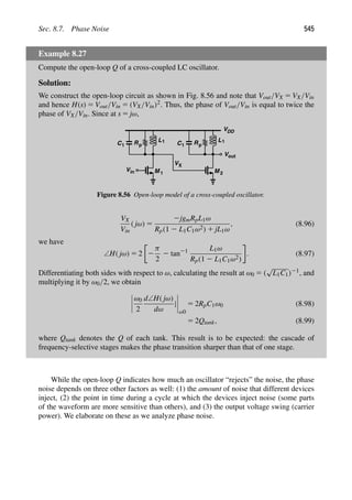
![546 Chap. 8. Oscillators
H ( )
s Y
X
Noise SX
Δω Δω
0
(a) (b)
Figure 8.57 (a) Oscillator model, (b) noise shaping in oscillator.
Noise Shaping in Oscillators As our first step toward formulating the phase noise, we
wish to understand what happens if noise is injected into an oscillatory circuit. Employing
the feedback model, we represent the noise as an additive term [Fig. 8.57(a)] and write
Y(s)
X(s)
5
H(s)
1 1 H(s)
. (8.100)
In the vicinity of the oscillation frequency, i.e., at ω 5 ω0 1 ω, we can approximate
H( jω) with the first two terms in its Taylor series:
H( jω) ≈ H( jω0) 1 ω
dH
dω
. (8.101)
If H( jω0) 5 21 and ωdH/dω 1, then Eq. (8.100) reduces to
Y
X
( jω0 1 j ω) ≈
21
ω
dH
dω
. (8.102)
In other words, as shown in Fig. 8.57(b), the noise spectrum is “shaped” by
Y
X
( jω0 1 j ω)
2
5
1
ω2
|
dH
dω
|2
. (8.103)
To determine the shape of |dH/dω|2, we write H( jω) in polar form, H( jω) 5 |H| exp( jφ)
and differentiate with respect to ω,
dH
dω
5
d|H|
dω
1 j|H|
dφ
dω
exp( jφ). (8.104)
It follows that
dH
dω
2
5
d|H|
dω
2
1
dφ
dω
2
|H|2
. (8.105)
This equation leads to a general definition of Q [4], but we limit our study here to simple
LC oscillators. Note that (a) in an LC oscillator, the term |d|H|/dω|2 is much less than](https://image.slidesharecdn.com/rfmicroelectronicsrazavi-230814101614-71259b59/85/RF-MICROELECTRONICS_Razavi-pdf-571-320.jpg)
![Sec. 8.7. Phase Noise 547
|dφ/dω|2 in the vicinity of the resonance frequency, and (b) |H| is close to unity for steady
oscillations. The right-hand side of Eq. (8.105) therefore reduces to |dφ/dω|2, yielding
Y
X
( jω0 1 j ω)
2
5
1
ω2
0
4
dφ
dω
2
ω2
0
4 ω2
. (8.106)
From (8.95),
Y
X
( jω0 1 j ω)
2
5
1
4Q2
ω0
ω
2
. (8.107)
Known as “Leeson’s Equation” [3], this result reaffirms our intuition that the open-loop Q
signifies how much the oscillator rejects the noise.
Example 8.28
A student designs the cross-coupled oscillator of Fig. 8.58 with 2/gm 5 2Rp, reasoning that
the tank now has infinite Q and hence the oscillator produces no phase noise!6
Explain
the flaw in this argument. (This circuit is similar to that in Fig. 8.21(b), but with the tank
components renamed.)
C1
M
M 2
1
I SS
Y
X
Rp
L1
Rp
−
Figure 8.58 Apparently infinite Q in an oscillator.
Solution:
The Q in Eq. (8.107) is the open-loop Q, i.e., ω0/2 times the slope of the phase of the
open-loop transfer function, which was calculated in Example 8.27. The “closed-loop” Q
does not carry much meaning.
6. The center tap of L1 is tied to VDD but not shown.](https://image.slidesharecdn.com/rfmicroelectronicsrazavi-230814101614-71259b59/85/RF-MICROELECTRONICS_Razavi-pdf-572-320.jpg)
![548 Chap. 8. Oscillators
H ( )
s Y
X
( )
s
G
Figure 8.59 Noise shaping in a general oscillator.
In Problem 8.11, we prove that, if the feedback path has a transfer function G(s)
(Fig. 8.59), then
Y
X
( jω0 1 j ω)
2
5
1
4Q2
ω0
ω
2 1
G( jω0)
2
, (8.108)
where the open-loop Q is given by
Q 5
ω0
2
d(GH)
dω
. (8.109)
Linear Model The foregoing development suggests that the total noise at the output of an
oscillator can be obtained according to a number of transfer functions similar to Eq. (8.107)
from each noise source to the output. Such an approach begins with a small-signal (linear)
model and can account for some of the nonidealities [4]. However, the small-signal model
may ignore some important effects, e.g., the noise of the tail current source, or face other
difficulties. The following example illustrates this point.
Example 8.29
Compute the total noise injected to the differential output of the cross-coupled oscillator
when the transistors are in equilibrium. Note that the two-sided spectral density of the drain
current noise is equal to I2
n 5 2kTγ gm.
Solution:
Let us first determine the Norton equivalent of the cross-coupled pair. From Fig. 8.60(a),
the reader can show that the short-circuit output current, IX, is equal to half of the noise
current of each transistor: IX 5 (In2 2 In1)/2. Thus, as shown in Fig. 8.60(b), the output
noise is obtained as
V2
n,out 5
I2
X 1
2kT
Rp
R2L2
1ω2
R2(1 2 L1C1ω2)2 1 L2
1ω2
, (8.110)](https://image.slidesharecdn.com/rfmicroelectronicsrazavi-230814101614-71259b59/85/RF-MICROELECTRONICS_Razavi-pdf-573-320.jpg)
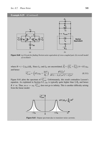
![550 Chap. 8. Oscillators
Conversion of Additive Noise to Phase Noise The result expressed by (8.107) and exem-
plified by (8.111) yields the total noise that is added to the oscillation waveform at the
output. We must now determine how and to what extent additive noise corrupts the phase.
Let us begin with the simple case depicted in Fig. 8.62(a). The carrier appears at ω0 and
the additive noise in a 1-Hz bandwidth centered at ω0 1 ω is modeled by an impulse. In
the time domain, the overall waveform is x(t) 5 A cos ω0t 1 a cos(ω0 1 ω)t where a A.
Intuitively, we expect the additive component to produce both amplitude and phase modu-
lation. To understand this point, we represent the carrier by a phasor of magnitude A that
rotates at a rate of ω0 [Fig. 8.62(b)]. The component at ω0 1 ω adds vectorially to the
carrier, i.e., it appears as a small phasor at the tip of the carrier phasor and rotates at a rate
of ω0 1 ω. At any point in time, the small phasor can be expressed as the sum of two
other phasors, one aligned with A and the other perpendicular to it. The former modulates
the amplitude and the latter, the phase. Figure 8.62(c) illustrates the behavior in the time
domain.
ω0 ω0 ω
+ Δω
A
a A
a
θ
Amplitude
Modulation
Modulation
Phase
t
)
(t
x
Amplitude
Modulation
Modulation
Phase
(a) (b) (c)
Figure 8.62 (a) Addition of a small sideband to a sinusoid, (b) phasor diagram showing both AM
and PM, (c) time-domain waveform.
In order to compute the phase modulation resulting from a small sinusoid at ω0 1 ω,
we make two important observations. First, as described in Chapter 3, the spectrum of
Fig. 8.62(a) can be written as the sum of an AM signal and an FM signal. Second, the
phase of the overall signal is obtained by applying the composite signal to a hard limiter,
i.e., a circuit that clips the amplitude and hence removes AM. From Chapter 3, the output
of the limiter can be written as
xlim(t) 5
A
2
cos ω0t 2
a
2
cos(ω0 1 ω)t 1
a
2
cos(ω0 2 ω)t (8.112)
≈
A
2
cos
ω0t 2
2a
A
sin ωt
. (8.113)
We recognize the phase component, (2a/A) sin ωt, as simply the original additive com-
ponent at ω0 1 ω, but translated down by ω0, shifted by 908, and normalized to A/2. We
therefore expect that narrowband random additive noise in the vicinity of ω0 results in a
phase whose spectrum has the same shape as that of the additive noise but translated by ω0
and normalized to A/2.
This conjecture can be proved analytically. We write x(t) 5 A cos ω0t 1 n(t), where
n(t) denotes the narrowband additive noise (voltage or current). It can be proved that](https://image.slidesharecdn.com/rfmicroelectronicsrazavi-230814101614-71259b59/85/RF-MICROELECTRONICS_Razavi-pdf-575-320.jpg)
![Sec. 8.7. Phase Noise 551
narrowband noise in the vicinity of ω0 can be expressed in terms of its quadrature
components [9]:
n(t) 5 nI(t) cos ω0t 2 nQ(t) sin ω0t, (8.114)
where nI(t) and nQ(t) have the same spectrum, which [for real n(t)] is equal to the spectrum
of n(t) but translated down by ω0 (Fig. 8.63) and doubled in spectral density. It follows that
x(t) 5 [A 1 nI(t)] cos ω0t 2 nQ(t) sin ω0t. (8.115)
ω
ω
S
0
n ( )
ω
0
+
ω0
−
η
ω
S ( )
ω
0
η
nI
S ( )
ω
nQ ,
2
Figure 8.63 Narrowband noise and spectrum of its quadrature components.
Expressing Eq. (8.115) in polar form, we have
x(t) 5
[A 1 nI(t)]2 1 n2
Q(t) cos ω0t 1 tan21 nQ(t)
A 1 nI(t)
. (8.116)
Since nI(t), nQ(t) A, the phase component is equal to
φn(t) ≈
nQ(t)
A
, (8.117)
as postulated previously. It follows that
Sφn(ω) 5
SnQ(ω)
A2
. (8.118)
Note that A is the peak (not the rms) amplitude of the carrier. In Problem 8.12, we prove
that half of the noise power is carried by the AM sidebands and the other half by the PM
sidebands.
We are ultimately interested in the spectrum of the RF waveform, x(t), but excluding
its AM noise. We have
x(t) ≈ A cos ω0t 1
nQ(t)
A
(8.119)
≈ A cos ω0t 2 nQ(t) sin ω0t. (8.120)
Thus, the power spectral density of x(t) consists of two impulses at ±ω0, each with a power
of A2/4, and SnQ/4 centered around ±ω0. As shown in Fig. 8.64, a spectrum analyzer folds](https://image.slidesharecdn.com/rfmicroelectronicsrazavi-230814101614-71259b59/85/RF-MICROELECTRONICS_Razavi-pdf-576-320.jpg)
![552 Chap. 8. Oscillators
ω
0
η
ω
ω
0
+
ω
−
η
ω
Spectrum
ω
Additive
Noise
Measured
0 0
2
Quadrature
Noise Spectrum
ω
0
S ( )
ω
φn
ω
ω
0
+
ω
− 0 0
η
2
A
2
η
A
2
2
η
A
2
Spectrum of
)
(t
x
4
A
2
4
(Normalized to 2
0
Carrier Power)
Figure 8.64 Summary of conversion of additive noise to phase noise.
the negative- and positive-frequency contents. After the folding, we normalize the phase
noise to the total carrier power, A2/2.
The foregoing development can be summarized as follows (Fig. 8.64). Additive noise
around ±ω0 having a two-sided spectral density with a peak of η results in a phase noise
spectrum around ω0 having a normalized one-sided spectral density with a peak of 2η/A2,
where A is the peak amplitude of the carrier.
Cyclostationary Noise The derivations leading to Eq. (8.111) have assumed that the noise
of each transistor can be represented by a constant spectral density; however, as the tran-
sistors experience large-signal excursions, their transconductance and hence noise power
varies. Since oscillators perform this noise modulation periodically, we say such noise
sources are “cyclostationary,” i.e., their spectrum varies periodically. We begin our anal-
ysis with an observation made in Chapter 6 regarding cyclostationary white noise: white
noise multiplied by a periodic envelope in the time domain remains white. For example, if
white noise is switched on and off with 50% duty cycle, the result is still white but has half
the spectral density.
In order to study the effect of cyclostationary noise, we return to the original cross-
coupled oscillator and, from Fig. 8.65(a), recognize that (1) when VX reaches a maximum
and VY a minimum, M1 turns off, injecting no noise; (2) when M1 and M2 are near equilib-
rium, they inject maximum noise current, with a total two-sided spectral density of kTγ gm,
where gm is the equilibrium transconductance; (3) when VX reaches a minimum and VY
a maximum, M1 is on but degenerated by the tail current (while M2 is off), injecting
little noise to the output. We therefore conclude that the total noise current experiences
an envelope having twice the oscillation frequency and swinging between zero and unity
[Fig. 8.65(b)].](https://image.slidesharecdn.com/rfmicroelectronicsrazavi-230814101614-71259b59/85/RF-MICROELECTRONICS_Razavi-pdf-577-320.jpg)
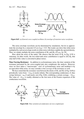
![554 Chap. 8. Oscillators
What can we say about 2Gavg? If 2Gavg is not sufficient to compensate for the loss
of the tank, Rp, then the oscillation decays. Conversely, if 2Gavg is more than enough,
then the oscillation amplitude grows. In the steady state, therefore, Gavg 5 1/Rp. This is
a powerful observation: regardless of the transistor dimensions and the value of the tail
current, Gavg must remain equal to Rp.
Example 8.30
What happens to the conductance waveform and Gavg if the tail current is increased?
Solution:
Since Gavg must remain equal to 1/Rp, the waveform changes shape such that it has greater
excursions but still the same average value. As shown in Fig. 8.67(a), a larger tail cur-
rent leads to a greater peak transconductance, 2gm2/2, while increasing the time that the
transconductance spends near zero so that the average is constant. That is, the transistors
are at equilibrium for a shorter amount of time [Fig. 8.67(b)].
t
t
Average
Transconductance
G
g
−
0
2
m1
g
−
2
m2
Gavg
−
I
I
D1
D2
Figure 8.67 Effect of increasing tail current on (a) transconductance, and (b) oscillation wave-
forms.
Phase Noise Computation We now consolidate our formulations of (a) conversion of
additive noise to phase noise, (b) cyclostationary noise, and (c) time-varying resistance.
Our analysis proceeds as follows:
1. We compute the average spectral density of the noise current injected by the cross-
coupled pair. If a sinusoidal envelope is assumed, the two-sided spectral density
amounts to kTγ gm 3 (3/8), where gm denotes the equilibrium transconductance of
each transistor.
2. To this we add the noise current of Rp, obtaining (3/8)kTγ gm 1 2kT/Rp.](https://image.slidesharecdn.com/rfmicroelectronicsrazavi-230814101614-71259b59/85/RF-MICROELECTRONICS_Razavi-pdf-579-320.jpg)
![Sec. 8.7. Phase Noise 555
3. We multiply the above spectral density by the squared magnitude of the net
impedance seen between the output nodes. Since Gavg 5 1/Rp, the average resis-
tance is infinite, leaving only L1 and C1 in Fig. 8.65(a). That is,
V2
n,out 5 kT
3
8
γ gm 1
2
Rp
L2
1ω2
(1 2 L1C1ω2)2
, (8.121)
which, for ω 5 ω0 1 ω and ω ω0, reduces to
V2
n,out 5 kT
3
8
γ gm 1
2
Rp
1
4C2
1 ω2
. (8.122)
The factor of 3/8 depends on the noise envelope waveform and must be obtained by
careful simulations.
4. From Fig. 8.64, we divide this result by A2/2 to obtain the one-sided phase noise
spectrum around ω0. Note that in Fig. 8.65(a), A 5 (4/π)(ISSRp/2) 5 (2/π)ISS/Rp
and Rp 5 QL1ω0.7
It follows that
S( ω) 5
π2
2
kT
I2
SS
3
8
γ gm 1
2
Rp
ω2
0
4Q2 ω2
. (8.123)
As the tail current and hence the output swings increase, I2
SS rises much more sharply
than gm, thereby lowering the phase noise (so long as the transistors do not enter
the deep triode region).
A closer examination of the cross-coupled oscillator reveals that the phase noise is in
fact independent of the transconductance of the transistors [10, 11, 17]. This can be quali-
tatively justified as follows. Suppose the widths of the two transistors are increased while
the output voltage swing and frequency are kept constant. The transistors can now steer
their tail current with a smaller voltage swing, thus experiencing sharper current switching
(Fig. 8.68). That is, M1 and M2 spend less time injecting noise into the tank. However, the
higher transconductance translates to a higher amount of injected noise, as evident from
the noise envelope. It turns out that the decrease in the width and the increase in the height
of the noise envelope pulses cancel each other, and gm can be simply replaced with 2/Rp in
the above equation [10, 11, 17]:
S( ω) 5
π2
Rp
kT
I2
SS
3
8
γ 1 1
ω2
0
4Q2 ω2
. (8.124)
Problem of Tail Capacitance What happens if one of the transistors enters the deep
triode region? As depicted in Fig. 8.69(a), the corresponding tank is temporarily con-
nected to the tail capacitance through the on-resistance of the transistor, degrading the Q.
7. The differential resistance, Rp, can be viewed as two resistors of value Rp/2 tied to VDD. The peak single-
ended swing is therefore equal to (2/π)(Rp/2)ISS.](https://image.slidesharecdn.com/rfmicroelectronicsrazavi-230814101614-71259b59/85/RF-MICROELECTRONICS_Razavi-pdf-580-320.jpg)
![556 Chap. 8. Oscillators
t
M 1
I
I
D1
D2
Wider
Transistors
Noise Envelope
of
Wider
Transistors
Figure 8.68 Oscillator waveforms for different transistor widths.
L R C
M
VDD
R L
C
M 1 2
1
1 1 1
I SS CT
Ron
L R C
1 1 1 RT CT
(a) (b)
1 1
Figure 8.69 (a) Oscillator with one transistor in deep triode region, (b) equivalent circuit of the
tank.
Transforming the series combination of Ron and CT to a parallel circuit, we obtain the
equivalent network shown in Fig. 8.69(b), where RT 5 (RonC2
Tω2
0)21. If RT is comparable
to R1 and each transistor remains in the deep triode region for an appreciable fraction of
the period, then the Q degrades significantly. Equivalently, the noise injected by M2 rises
considerably [17].
The key result here is that, as the tail current is increased, the (relative) phase noise
continues to decline up to the point where the transistors enter the triode region. Beyond
this point, a higher tail current raises the output swing more gradually, but the overall tank Q
begins to fall, yielding no significant improvement in the phase noise. Of course, this trend
depends on the value of CT and may be pronounced only in some designs. This capacitance
may be large due to the parasitics of ISS or it may be added deliberately to shunt the noise
of ISS to ground (Section 8.7.5).](https://image.slidesharecdn.com/rfmicroelectronicsrazavi-230814101614-71259b59/85/RF-MICROELECTRONICS_Razavi-pdf-581-320.jpg)
![Sec. 8.7. Phase Noise 557
Example 8.31
How does the above phenomenon manifest itself in the top-biased topology of Fig. 8.30(a)?
Solution:
In this case, each transistor entering the deep triode region provides a direct resistive path
to ground. Since node P is also at (ac) ground, the tank Q heavily deteriorates. We thus
expect this topology to suffer more severely if M1 or M2 enters the deep triode region.
8.7.4 Analysis of Phase Noise: Approach II
The approach described in this section follows that in [6]. Consider an ideal LC tank that,
due to an initial condition, produces a sinusoidal output [Fig. 8.70(a)]. During the oscilla-
tion, L1 and C1 exchange the initial energy, with the former carrying the entire energy at
the zero crossings and the latter, at the peaks. Let us assume that the circuit begins with an
initial voltage of V0 across the capacitor. Now, suppose an impulse of current is injected
into the oscillating tank at the peak of the output voltage [Fig. 8.70(b)], producing a voltage
step across C1. If 8
Iin(t) 5 I1δ(t 2 t1), (8.125)
then the additional energy gives rise to a larger oscillation amplitude:
Vp 5 V0 1
I1
C1
. (8.126)
L C
1 1 out
V
I in
t
Vout
V0
Vp
I
C1
1
I 1 )
(t
δ
Vout
V0
t
t
t
I
C1
1
t 1 t 2
(a) (b) (c)
I in
t
− 1
I in I 1 )
(t
δ t
− 2
Figure 8.70 (a) Ideal tank with a current impulse, (b) effect of impulse injection at peak of
waveform, (c) effect of impulse injection at zero crossing of waveform.
8. Note that I1 in this equation is in fact a charge quantity because it denotes the area under the impulses.](https://image.slidesharecdn.com/rfmicroelectronicsrazavi-230814101614-71259b59/85/RF-MICROELECTRONICS_Razavi-pdf-582-320.jpg)
![558 Chap. 8. Oscillators
The key point here is that the injection at the peak does not disturb the phase of the
oscillation (as shown in the example below).
Next, let us assume the impulse of current is injected at a zero crossing point. A voltage
step is again created but leading to a phase jump [Fig. 8.70(c)]. Since the voltage jumps
from 0 to I1/C1, the phase is disturbed by an amount equal to sin21
[I1/(C1V0)]. We there-
fore conclude that noise creates only amplitude modulation if injected at the peaks and only
phase modulation if injected at the zero crossings.
Example 8.32
Explain how the effect of the current impulse can be determined analytically.
Solution:
The linearity of the tank allows the use of superposition for the injected currents (the inputs)
and the voltage waveforms (the outputs). The output waveform consists of two sinusoidal
components, one due to the initial condition9
(the oscillation waveform) and another due
to the impulse. Figure 8.71 illustrates these components for two cases: if injected at t1, the
impulse leads to a sinusoid exactly in phase with the original component, and if injected at
t2, the impulse produces a sinusoid 908 out of phase with respect to the original component.
In the former case, the peaks are unaffected, and in the latter, the zero crossings.
t
t
t
t 1
t 2
Oscillation
Waveform
Waveform
Impulse−Induced
Waveform
Impulse−Induced
Figure 8.71 Computation of impulse response using superposition.
The foregoing observations suggest the need for a method of quantifying how and when
each source of noise in an oscillator “hits” the output waveform. While the transistors turn
on and off, a noise source may only appear near the peaks of the output voltage, contributing
9. The initial condition in the tank can also be created by a current impulse and hence does not make the system
nonlinear.](https://image.slidesharecdn.com/rfmicroelectronicsrazavi-230814101614-71259b59/85/RF-MICROELECTRONICS_Razavi-pdf-583-320.jpg)
![Sec. 8.7. Phase Noise 559
negligible phase noise, whereas another may hit the zero crossings, producing substantial
phase noise. To this end, we define a linear, time-variant system from each noise source
to the output phase. The linearity property is justified because the noise levels are very
small, and the time variance is necessary to capture the effect of the time at which the noise
appears at the output.
For a linear, time-variant system, the convolution property holds, but the impulse
response varies with time. Thus, the output phase in response to a noise n(t) is given by
φ(t) 5 h(t, τ) ∗ n(t), (8.127)
where h(t, τ) is the time-variant impulse response from n(t) to φ(t). In an oscillator, h(t, τ)
varies periodically: as illustrated in Fig. 8.72, a noise impulse injected at t 5 t1 or integer
multiples of the period thereafter produces the same phase change. Now, the task of output
phase noise calculation consists of computing h(t, τ) for each noise source and convolving
it with the noise waveform. The impulse response, h(t, τ), is called the “impulse sensitivity
function” (ISF) in [6].
t
t
t1 t1+Tc
Vout Vout
Figure 8.72 Periodic impulse response in an oscillator.
Example 8.33
Explain how the LC tank of Fig. 8.70(a) has a time-variant behavior even though the
inductor and the capacitor values remain constant.
Solution:
The time variance arises from the finite initial condition (e.g., the initial voltage across
C1). With a zero initial condition, the circuit begins with a zero output, exhibiting a time-
invariant response to the input.
Example 8.34
Compute the phase impulse response for the lossless LC tank of Fig. 8.70(a).
Solution:
We invoke the superposition perspective of Example 8.32 and wish to calculate the phase
change resulting from a current impulse at an arbitrary time t1 (Fig. 8.73). The overall
output voltage can be expressed as
Vout(t) 5 V0 cos ω0t 1 V[cos ω0(t 2 t1)]u(t 2 t1), (8.128)
(Continues)](https://image.slidesharecdn.com/rfmicroelectronicsrazavi-230814101614-71259b59/85/RF-MICROELECTRONICS_Razavi-pdf-584-320.jpg)
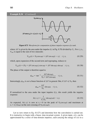
![Sec. 8.7. Phase Noise 561
t
)
(t
x
t
t
( t
− )
h n
Σ
t
)
(t
y
t
)
(t
x
t
hn
Σ
t
)
(t
y
h1
h2
hn
(a) (b)
t1 t2 tn t1 t2 tn
Figure 8.74 Convolution in a (a) time-invariant, and (b) time-variant linear system.
short time span [Fig. 8.74(a)]:
x(t) ≈
1 ∞
n 5 2∞
x(tn)δ(t 2 tn). (8.134)
Each impulse produces the time-invariant impulse response of the system at tn. Thus,
y(t) consists of time-shifted replicas of h(t), each scaled in amplitude according to the
corresponding value of x(t):
y(t) ≈
1 ∞
n 5 2∞
x(tn)h(t 2 tn) (8.135)
5
1 ∞
2∞
x(τ)h(t 2 τ)dτ. (8.136)
Now, consider the time-variant system shown in Fig. 8.74(b). In this case, the time-shifted
versions of h(t) may be different, and we denote them by h1(t), h2(t), . . ., hn(t), with the
understanding that hj(t) is the impulse response in the vicinity of tj. It follows that
y(t) ≈
1 ∞
n 5 2∞
x(tn)hn(t). (8.137)
How do we express these impulse responses as a continuous-time function? We simply
write them as h(t, τ), where τ is the specific time shift. For example, h1(t) 5 h(t, 1 ns),
h2(t) 5 h(t, 2 ns), etc. Thus,
y(t) 5
1 ∞
2∞
x(τ)h(t, τ)dτ. (8.138)](https://image.slidesharecdn.com/rfmicroelectronicsrazavi-230814101614-71259b59/85/RF-MICROELECTRONICS_Razavi-pdf-586-320.jpg)
![562 Chap. 8. Oscillators
Example 8.35
Determine the phase noise resulting from a current, in(t), having a white spectrum, Si( f),
that is injected into the tank of Fig. 8.70(a).
Solution:
From Eqs. (8.133) and (8.138),
φn(t) 5
1 ∞
2∞
in(τ)
1
C1V0
sin ω0τu(t 2 τ)dτ (8.139)
5
1
C1V0
t
2∞
in(τ) sin ω0τdτ. (8.140)
If in(t) is white, so is g(t) 5 in(t) sin ω0t (why?), but with half the spectral density of in(t):
Sg( f) 5
1
2
Si( f). (8.141)
Our task therefore reduces to finding the transfer function of the system shown in
Fig. 8.75(a). To this end, we note that (1) the impulse response of this system is simply
equal to (C1V0)21u(t), and (2) the Fourier transform of u(t) is given by ( jω)21 1 πδ(ω).
We ignore πδ(ω) as it contains energy at only ω 5 0 and write
Sφn( f) 5 |H( jω)|2
Sg( f) (8.142)
5
1
C2
1V2
0
1
(2πf)2
Si( f)
2
. (8.143)
C1V0
1
( )
ω
H
)
(t
g φ (t
n )
f
0
(a) (b)
)
(
S f
φn
Figure 8.75 (a) Equivalent system for conversion of g(t) to φn(t), (b) resulting phase noise
spectrum.
As expected, the relative phase noise is inversely proportional to the oscillation peak ampli-
tude, V0. Depicted in Fig. 8.75(b), this equation agrees with the noise-shaping concept
described in Section 8.7.3: the spectrum of A cos[ω0t 1 φn(t)] contains Sφn( f) but shifted
to a center frequency of ±ω0. Figure 8.76 summarizes the mechanisms that convert the](https://image.slidesharecdn.com/rfmicroelectronicsrazavi-230814101614-71259b59/85/RF-MICROELECTRONICS_Razavi-pdf-587-320.jpg)
![Sec. 8.7. Phase Noise 563
Example 8.35 (Continued)
injected noise current to phase noise. For clarity, the white noise near ±ω0 is shown as
three narrowband segments.
S
+
ω
−
ω
ω
0
ω 0
0
( )
ω
i
ω
− 0
0 ω0
+
ω
( )
ω
0
Sg
ω
( )
ω
0
Sφn
ω
ω0
Spectrum of
t
ω
A cos [ + φ (t
n )]
0
Figure 8.76 Summary of conversion of injected noise to phase noise around the carrier.
The reader may find the foregoing example confusing: if the lossless tank with its
nonzero initial condition is viewed as an oscillator with infinite Q, why is the phase noise
not zero? This confusion is resolved if we recognize that, as Q → ∞, the width and bias
current of the transistor needed to sustain oscillation become infinitesimally small. The
transistor thus injects nearly zero noise; i.e., if in(t) represents transistor noise, Si( f)
approaches zero.
Example 8.36
Which frequency components in in(t) in the above example contribute significant phase
noise?
Solution:
Since in(t) is multiplied by sin ω0t, noise components around ω0 are translated to the
vicinity of zero frequency and subsequently appear in Eq. (8.143) (Fig. 8.76). Thus, for
a sinusoidal phase impulse response (ISF), only noise frequencies near ω0 contribute sig-
nificant phase noise. The reader is encouraged to repeat the translations in Fig. 8.76 for a
low-frequency component in Si(ω).
Effect of Flicker Noise Due to its periodic nature, the impulse response of oscillators can
be expressed as a Fourier series:
h(t, τ) 5 [a0 1 a1 cos(ω0t 1 φ1) 1 a2 cos(2ω0t 1 φ2) 1 · · · ]u(t 2 τ), (8.144)](https://image.slidesharecdn.com/rfmicroelectronicsrazavi-230814101614-71259b59/85/RF-MICROELECTRONICS_Razavi-pdf-588-320.jpg)
![564 Chap. 8. Oscillators
where a0 is the average (or “dc”) value of h(t, τ). In the LC tank studied above, aj 5 0
for all j 5 1, but in general this may not be true. In particular, suppose a0 5 0. Then, the
corresponding phase noise in response to an injected noise in(t) is equal to
φn,a0 5
t
2∞
a0in(τ)dτ. (8.145)
From Example 8.35, the integration is equivalent to a transfer function of ( jω)21 and hence
Sφn,a0( f) 5
a2
0
ω2
Si( f). (8.146)
That is, low-frequency components in in(t) contribute phase noise. (Recall that Sφn,a0 is
upconverted to a center frequency of ω0.) The key point here is that, if the “dc” value of
h(t, τ) is nonzero, then the flicker noise of the MOS transistors in the oscillator generates
phase noise. For flicker noise, we employ the gate-referred noise voltage expression given
by Sv( f) 5 [K/(WLCox)]/f and write
Sφn,a0( f) 5
a2
0
4π2
K
WLCox
1
f3
. (8.147)
Note that in this case, a0 represents the dc term of the impulse response from the gate
voltage of the transistors to the output phase. Since a0 relates to the symmetry of h(t, τ),
low upconversion of 1/f noise requires a circuit design that exhibits an odd-symmetric
h(t, τ) [6]. However, the 1/f noise of different transistors in the circuit may see different
impulse responses, and it may therefore be impossible to minimize the upconversion of all
1/f noise sources. For example, in the circuit of Fig. 8.35, it is possible to make h(t, τ)
from the gates of M1-M4 to the output symmetric, but not from the tail current source to
the output. As ISS slowly fluctuates, so does the output CM level and hence the oscillation
frequency. In general, the phase noise spectrum assumes the shape shown in Fig. 8.77.
Noise around Higher Harmonics Let us now turn our attention to the remaining
terms in Eq. (8.144). As mentioned in Example 8.35, a1 cos(ω0t 1 φ1) translates noise
frequencies around ω0 to the vicinity of zero and into phase noise. By the same
token, am cos(mω0t 1 φj) converts noise components around mω0 in in(t) to phase noise.
Figure 8.78 illustrates this behavior [6].
0
1
f 3
1
f 2
Δf
Figure 8.77 Phase noise profile showing regions arising from flicker and white noise.](https://image.slidesharecdn.com/rfmicroelectronicsrazavi-230814101614-71259b59/85/RF-MICROELECTRONICS_Razavi-pdf-589-320.jpg)
![Sec. 8.7. Phase Noise 565
0
Flicker
Noise
Noise
White
f
f0 f0
2
S ( )
i
f
0 f
Sφn( )
f
Figure 8.78 Conversion of various noise components to phase noise.
Cyclostationary Noise We must also incorporate the effect of cyclostationary noise. As
explained in Section 8.7.3, such noise can be viewed as stationary noise, n(t), multiplied
by a periodic envelope, e(t). Equation (8.138) can thus be written as
y(t) 5
1 ∞
2∞
n(τ)e(τ)h(t, τ)dτ, (8.148)
implying that e(t)h(t, τ) can be viewed as an “effective” impulse response [6]. In other
words, the effect of n(t) on phase noise ultimately depends on the product of the cyclo-
stationary noise envelope and h(t, τ).
This approach to phase noise analysis generally requires that both the noise envelope
and the impulse response be determined from multiple simulations for each device. Design
optimization may therefore prove a lengthy task.
Each of the two analysis approaches described thus far imparts its own insights and
finds its own utility in circuit design. However, there are other phase noise mechanisms
that can be better understood by other analysis techniques. The next section is an example.
8.7.5 Noise of Bias Current Source
Oscillators typically employ a bias current source so as to minimize sensitivity to the supply
voltage and noise therein. We wish to study the phase noise contributed by this current
source. Figure 8.79 summarizes the tail-related noise mechanisms studied here.
Consider the topology shown in Fig. 8.80(a), where In models the noise of ISS, includ-
ing flicker noise near zero frequency, thermal noise around the oscillation frequency, ω0,](https://image.slidesharecdn.com/rfmicroelectronicsrazavi-230814101614-71259b59/85/RF-MICROELECTRONICS_Razavi-pdf-590-320.jpg)
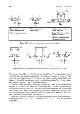
![Sec. 8.7. Phase Noise 567
ω0 ω
+2
0
−2ω
Δω
ω0
ω
ω0
+3
0
I n
ω0 ω
Δω
Δω
0
ω0 ω
I
2
0
+
I 0
−
6
ω0 ω
I 0
+
I 0
−
6
6
ω0 ω
I 0
+
3
+
ω0
I 0
+
I 0
−
6
6
PM
ω0
I 0
+
6
ω
ω
AM I 0
+
6
(a)
(b)
Figure 8.81 (a) Translation of tail noise around 2ω0 to sidebands around ω0, (b) separation of
PM and AM components.
The noise around 2ω0, on the other hand, markedly impacts the performance [12, 7].
As illustrated in Fig. 8.81(a), a noise component slightly below 2ω0 is mixed with the
first and third harmonics of the square wave, thereby falling at slightly below and above
ω0 but with different amplitudes and polarities. To determine whether these components
produce AM or FM, we express the oscillator output as cos ω0t and its third harmonic as
(21/3) cos(3ω0t). For a tail current noise component, I0 cos(2ω0 2 ω)t, the differential
output current of M1 and M2 emerges as
Iout ∝ cos ω0tI0 cos(2ω0 2 ω)t 1
21
3
cos(3ω0t)I0 cos(2ω0 2 ω)t (8.149)
∝
I0
2
cos(ω0 2 ω)t 2
I0
6
cos(ω0 1 ω)t 1 . . . . (8.150)
As explained in Chapter 3, two equal cosine sidebands having opposite signs sur-
rounding a cosine carrier represent FM. In the above equation, however, the two side-
bands have unequal magnitudes, creating some AM as well. Writing (I0/2) cos(ω0 2
ω)t 5 (I0/6) cos(ω0 2 ω)t 1 (I0/3) cos(ω0 2 ω)t and extracting from the second term
its PM components [Fig. 8.81(b)] as (I0/6) cos(ω0 2 ω)t 2 (I0/6) cos(ω0 1 ω)t, we
obtain the overall PM sidebands:
Iout ∝
I0
3
cos(ω0 1 ω)t 2
I0
3
cos(ω0 2 ω)t 1 . . . . (8.151)
The proportionality factor is related to the conversion gain of the mixing action, as
illustrated by the following example.](https://image.slidesharecdn.com/rfmicroelectronicsrazavi-230814101614-71259b59/85/RF-MICROELECTRONICS_Razavi-pdf-592-320.jpg)
![568 Chap. 8. Oscillators
Example 8.37
For a tail noise of In 5 I0 cos(2ω0 1 ω)t in Fig. 8.80(a), determine the magnitude of the
FM sidebands in the differential output current.
Solution:
In the frequency domain, each impulse near 2ω0 has a magnitude of I0/2. Upon mixing
with the first harmonic of the square wave, the impulse at 2ω0 1 ω appears at ω0 1 ω
with a height of (2/π)(I0/2). Similarly, mixing with the third harmonic yields an impulse at
ω0 2 ω with a height of 2(1/3)(2/π)(I0/2). Separating the AM component as explained
above, we have
Iout 5
1
3
4
π
I0 cos(ω0 1 ω)t 2
1
3
4
π
I0 cos(ω0 2 ω)t 1 . . . . (8.152)
To obtain the phase noise in the output voltage, (1) the current sidebands computed in
the above example must be multiplied by the impedance of the tank at a frequency offset
of ± ω, and (2) the result must be normalized to the oscillation amplitude. Note that the
current components see the lossless impedance of the tank once they are injected into the
output nodes because the average negative conductance presented by M1 and M2 cancels
the loss. This impedance is given by 2j/(2C1 ω) if ω ω0. Thus, the relative phase
noise can be expressed as
S( ω) 5
16I2
n
9π2
1
2C ω
2
4
π2
I2
SSR2
p
5
4I2
n
9I2
SS
ω0
2Q ω
2
. (8.153)
The thermal noise near higher even harmonics of ω0 plays a similar role, producing
FM sidebands around ω0. It can be shown that the summation of all of the sideband powers
results in the following phase noise expression due to the tail current source [8, 10]:
S( ω) 5
π2I2
n
16I2
SS
ω0
2Q ω
2
. (8.154)
Let us now consider the noise of the top current source in Fig. 8.30(a). We wish to
formulate the frequency modulation resulting from this noise. Suppose IDD contains a
noise current in(t). As calculated in Example 8.16, in(t) produces a common-mode voltage
change of
V 5
1
gm
in(t)
2
. (8.155)
This change is indistinguishable from an equal but opposite change in the control voltage,
Vcont. As explained in Section 8.10, the output waveform can be expressed as
Vout(t) 5 V0 cos ω0t 1
KVCO
in(t)
2gm
dt , (8.156)](https://image.slidesharecdn.com/rfmicroelectronicsrazavi-230814101614-71259b59/85/RF-MICROELECTRONICS_Razavi-pdf-593-320.jpg)
, producing
Sφn( f) 5
KVCO
2gm
1
2πf
2
α
f
. (8.158)
AM/PM Conversion Let us summarize our findings thus far. In the tail-biased oscillator
(and in the top-biased oscillator), the noise near zero frequency introduces amplitude mod-
ulation, whereas that near even harmonics of ω0 leads to phase noise. [In the top-biased
oscillator, low-frequency noise in the current source also modulates the output CM level,
producing phase noise (Example 8.16).]
The amplitude modulation resulting from the bias current noise does translate to phase
noise in the presence of nonlinear capacitances in the tanks [13, 14]. To understand this
point, we return to our AM/PM modulation study in Chapter 2 and make the follow-
ing observations. Since the varactor capacitance varies periodically with time, it can be
expressed as a Fourier series:
Cvar 5 Cavg 1
∞
n 5 1
an cos nω0t 1
∞
n 5 1
bn sin nω0t, (8.159)
where Cavg denotes the “dc” value. If noise in the circuit modulates Cavg, then the oscil-
lation frequency and phase are also modulated. We must therefore determine under what
conditions the tail noise, i.e., the output AM noise, modulates Cavg.
Consider the tank shown in Fig. 8.83(a), and first assume that the voltage dependence
of C1 is odd-symmetric around the vertial axis, e.g., C1 5 C0(1 1 αV). In this case, Cavg is
independent of the signal amplitude because the capacitance spends equal amounts of time
above and below C0 [Fig. 8.83(b)]. The average tank resonance frequency is thus constant
and no phase modulation occurs.
The above results change if C1 exhibits even-order voltage dependence, e.g.,
C1 5 C0(1 1 α1V 1 α2V2). Now, the capacitance changes more sharply for negative or
positive voltages, yielding an average that depends on the current amplitude [Fig. 8.83(c)].](https://image.slidesharecdn.com/rfmicroelectronicsrazavi-230814101614-71259b59/85/RF-MICROELECTRONICS_Razavi-pdf-594-320.jpg)
![570 Chap. 8. Oscillators
L C
1 1 out
V
I in Rp
(a)
t
C1
C0
Vout
t
C1
C0
t
Vout
C1
I in
Cavg
t
I in
C1
Cavg
(b) (c)
Figure 8.83 (a) Tank driven by an RF current course, (b) effect of AM on average capacitance for a
C/V characteristic that is symmetric around vertical axis, (c) effect of AM on average
capacitance for a C/V characteristic that is asymmetric around vertical axis.
We therefore observe that, in an oscillator employing such a tank, slow modulation of the
amplitude varies the average tank resonance frequency and hence the frequency of oscilla-
tion. The phase noise resulting from the low-frequency bias current noise is computed in
[13]. We study a simplified case in Problem 8.13.
It is important to note that the tail current in Fig. 8.35 introduces phase noise via three
distinct mechanisms: (1) its flicker noise modulates the output CM level and hence the
varactors; (2) its flicker noise produces AM at the output and hence phase noise through
AM/PM conversion; (3) its thermal noise at 2ω0 gives rise to phase noise.
8.7.6 Figures of Merit of VCOs
Our studies in this chapter point to direct trade-offs among the phase noise, power dis-
sipation, and tuning range of VCOs. For example, as explained in Chapter 7, varactors
themselves suffer from a trade-off between their capacitance range and their Q. We also
recall from Leeson’s equation, Eq. (8.107), that phase noise rises with the oscillation
frequency if the Q does not increase proportionally.
A figure of merit (FOM) that encapsulates some of these trade-offs is defined as
FOM1 5
(Oscillation Frequency)2
Power Dissipation 3 Phase Noise 3 (Offset Frequency)2
, (8.160)](https://image.slidesharecdn.com/rfmicroelectronicsrazavi-230814101614-71259b59/85/RF-MICROELECTRONICS_Razavi-pdf-595-320.jpg)
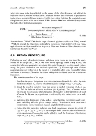
![572 Chap. 8. Oscillators
5. Using proper varactor models, determine the minimum capacitance of such a
varactor, Cvar,min, and compute the upper end of the tuning range,
ωmax 5
1
L0(CGS 1 4CGD 1 CDB 1 Cp 1 CL 1 Cvar,min)
. (8.163)
6. If ωmax is quite higher than necessary, increase Cvar,max in Eq. (8.162) so as to center
the tuning range around ω0.
The above procedure yields a design that achieves the maximum tuning range subject
to known values of ω0, the output swing, the power dissipation, and CL. If the varactor
Q is high enough, such a design also has the highest tank Q. At this point, we calculate
or simulate the phase noise for different frequencies across the tuning range. If the phase
noise rises significantly at ωmin or ωmax, then the tuning range must be reduced, and if it is
still excessively high, the design procedure must be repeated with a higher power budget.
In applications requiring a low phase noise, a multitude of different VCO topologies must
be designed and simulated so as to obtain a solution with an acceptable performance.
We carry out the detailed design of a 12-GHz VCO for 11a/g applications in Chapter 13.
Example 8.38
If the power budget allocated to the VCO topology of Fig. 8.25(a) is doubled, by what
factor is the phase noise reduced?
Solution:
Doubling the power budget can be viewed as (a) placing two identical oscillators in par-
allel [Fig. 8.84(a)] or (b) scaling all of the components in an oscillator by a factor of 2
[Fig. 8.84(b)]. In this scenario, the output voltage swing and the tuning range remain
unchanged (why?), but the phase noise power falls by a factor of two (3 dB). This is because
in Eq. (8.124), Rp is doubled and I2
SS is quadrupled.
I SS
C1
Rp
L1
W
L
W
L
I SS
C1
Rp
L1
W
L
W
L
I SS
C1
Rp
L1
W
L
2
/2
2
2
2
W
L
2
(a) (b)
Figure 8.84 Scaling of oscillator by (a) placing two instances in parallel, (b) scaling each
component.](https://image.slidesharecdn.com/rfmicroelectronicsrazavi-230814101614-71259b59/85/RF-MICROELECTRONICS_Razavi-pdf-597-320.jpg)
![Sec. 8.8. Design Procedure 573
8.8.1 Low-Noise VCOs
A great deal of effort has been expended on relaxing the trade-offs among phase
noise, power dissipation, and tuning range of VCOs. In this section, we study several
examples.
In order to reduce the phase noise due to flicker noise, the generic cross-coupled oscil-
lator can incorporate PMOS transistors rather than NMOS devices. Figure 8.85 depicts
the PMOS counterparts of the circuits shown in Figs. 8.25(a) and 8.30(a). Since PMOS
devices exhibit substantially less flicker noise, the close-in phase noise of these oscilla-
tors is typically 5 to 10 dB lower. The principal drawback of these topologies is their
limited speed, an issue that arises only as frequencies exceeding tens of gigahertz are
sought.
M v1 M v2
Vcont
VDD
M
M 3 4
L2
L1 M v1 M v2
Vcont
VDD
M
M 3 4
L2
L1
(a) (b)
Figure 8.85 (a) Tail-biased and (b) bottom-biased PMOS oscillators.
As explained in Section 8.7.5, the noise current at 2ω0 in the tail current source trans-
lates to phase noise around ω0. This and higher noise harmonics can be removed by a
capacitor as shown in Fig. 8.86(a). However, if M1 and M2 enter the deep triode region
during oscillation, then two effects raise the phase noise: (1) the on-resistance of each tran-
sistor now degrades the Q of the tank [Fig. 8.69(a)] [16], and (2) the impulse response (ISF)
from the noise of each transistor to the output phase becomes substantially larger [17]. This
I n
L
M
L
M 1 2
1
VDD
I SS
(a) (b)
CT
I n
L
M
L
M
1
VDD
I SS
CT
C1 C2
2
1
2
2
Vb
Figure 8.86 (a) Use of capacitor to shunt tail noise, (b) use of ac coupling to avoid operation in
deep triode region.](https://image.slidesharecdn.com/rfmicroelectronicsrazavi-230814101614-71259b59/85/RF-MICROELECTRONICS_Razavi-pdf-598-320.jpg)
![574 Chap. 8. Oscillators
issue can be resolved by means of two techniques. If operation in the triode region must be
avoided but large output swings are desired, capacitive coupling can be inserted in the loop
[Fig. 8.86(b)]. Here, Vb is chosen so that the peak voltage at the gate of each transistor does
not exceed its minimum drain voltage by more than one threshold. A Class-C oscillator
similar to this topology is described in [17].
Example 8.39
If C1 and C2 along with transistor capacitances attenuate the swing by a factor of 2,
determine the requisite value of Vb so that the transistors are in saturation.
Solution:
Illustrated in Fig. 8.87 are the gate and drain waveforms. For the transistor to remain in
saturation,
Vp
2
1 Vb 2 (VDD 2 Vp) ≤ VTH (8.164)
and hence
Vb ≤ VDD 2
3Vp
2
1 VTH. (8.165)
L
M 2
VDD
C2
2
Vb
VDD
VDD Vp
−
V
V
Vp
b
b
2
+
Figure 8.87 Gate and drain swings with capacitive coupling.
The bias voltage, Vb, in Fig. 8.86(b) must remain high enough to provide sufficient
VGS for the cross-coupled transistors and headroom for the tail current source. Conse-
quently, the output swings may still be severely limited. In Problem 8.14, we show that
the peak swing does not exceed approximately VDD 2 2(VGS 2 VTH). This is obtained
only if the capacitive attenuation is so large as to yield a negligible gate swing, requiring a
high gm.
The second approach is to allow M1 and M2 in Fig. 8.86(a) to enter the triode region
but remove the effect of the tail capacitance at 2ω0. Illustrated in Fig. 8.88 [16], the idea is
to insert inductor LT in series with the tail node and choose its value such that it resonates
with the parasitic capacitance, CB, at 2ω0. The advantage of this topology over that in
Fig. 8.86(b) is that it affords larger swings. The disadvantage is that it employs an additional
inductor and requires tail tuning for broadband operation.](https://image.slidesharecdn.com/rfmicroelectronicsrazavi-230814101614-71259b59/85/RF-MICROELECTRONICS_Razavi-pdf-599-320.jpg)
![Sec. 8.9. LO Interface 575
I n
L
M
L
M 1 2
1
VDD
I SS
2
L
CT
CB T
Figure 8.88 Use of tail resonance to avoid tank Q degradation in deep triode region.
Example 8.40
Study the behavior of the circuit shown in Fig. 8.88 if the supply voltage contains high-
frequency noise.
Solution:
Capacitor CB degrades the high-frequency common-mode rejection of the circuit. This
issue can be partially resolved by tying CB to VDD (Fig. 8.89). Now, CB bootstraps node
P to VDD at high frequencies. Of course, this is not possible if CB arises from only the
parasitics at the tail node.
I n
L
M
L
M 1 2
1
VDD
2
L1
CT
CB
P
I SS
Figure 8.89 Connection of capacitor to VDD to improve supply rejection.
8.9 LO INTERFACE
Each oscillator in an RF system typically drives a mixer and a frequency divider, expe-
riencing their input capacitances. Moreover, the LO output common-mode level must be
compatible with the input CM level of these circuits. We study this compatibility issue here.
The output CM level of the oscillators studied in this chapter is around VDD, VDD/2,
or zero [for the PMOS implementation of Fig. 8.85(a)]. On the other hand, the required](https://image.slidesharecdn.com/rfmicroelectronicsrazavi-230814101614-71259b59/85/RF-MICROELECTRONICS_Razavi-pdf-600-320.jpg)
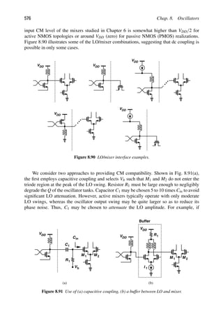
![Sec. 8.10. Mathematical Model of VCOs 577
VDD
M 1 M 2
(a) (b)
VDD
VDD
0
VDD
VDD
VDD
0
VDD
Figure 8.92 LO/divider interface for (a) current-steering and (b) rail-to-rail operation.
C1 5 Cin, an attenuation factor of 2 results and the capacitance presented to the LO falls to
C1Cin/(C1 1 Cin) 5 Cin/2, a useful attribute afforded by active mixers.
The second approach to CM compatibility interposes a buffer between the LO and
the mixer. In fact, if the mixer input capacitance excessively loads the LO, or if long,
lossy interconnects appear in the layout between the LO and the mixer, then such a buffer
proves indispensable. Depicted in Fig. 8.91(b) is an example, where an inductively-loaded
differential pair serves as a buffer, providing an output CM level equal to VDD 2 I1R1. This
value can be chosen to suit the LO port of the mixer. The drawback of this approach stems
from the use of additional inductors and the resulting routing complexity.
Similar considerations apply to the interface between an oscillator and a frequency
divider. For example, in Fig. 8.92(a), the divider input CM level must be well below VDD
to ensure the current-steering transistors M1 and M2 do not enter the deep triode region
(Chapter 10). As another example, some dividers require a rail-to-rail input [Fig. 8.92(b)],
and possibly capacitive coupling.
8.10 MATHEMATICAL MODEL OF VCOs
Our definition of voltage-controlled oscillators in Section 8.5 relates the output frequency
to the control voltage by a linear, static equation, ωout 5 ω0 1 KVCOVcont. But, how do we
express the output in the time domain? To this end, we must reexamine our understanding
of frequency and phase.
Example 8.41
Plot the waveforms for V1(t) 5 V0 sin ω1t and V2(t) 5 V0 sin(at2).
Solution:
To plot these waveforms carefully, we must determine the time instants at which the argu-
ment of the sine reaches integer multiples of π. For V1(t), the argument, ω1t, rises linearly
(Continues)](https://image.slidesharecdn.com/rfmicroelectronicsrazavi-230814101614-71259b59/85/RF-MICROELECTRONICS_Razavi-pdf-602-320.jpg)
![578 Chap. 8. Oscillators
Example 8.41 (Continued)
with time, crossing kπ at t 5 πk/ω1 [Fig. 8.93(a)]. For V2(t), on the other hand, the argu-
ment rises increasingly faster with time, crossing kπ more frequently. Thus, V2(t) appears
as shown in Fig. 8.93(b).
π
2π
π
π
4
3
V (t (
t
t
1
ω1t
ω1
π
2π
π
π
4
3
V (t (
t
t
t
π
π
π
5
6
7
π
8
a
2
2
(a (
) b)
Figure 8.93 (a) Linear and (b) quadratic growth of phase with time.
Example 8.42
Since a sinusoid of constant frequency ω1 can be expressed as V0 cos ω1t, a student
surmises that the output waveform of a VCO can be written as
Vout(t) 5 V0 cos ωoutt (8.166)
5 V0 cos(ω0 1 KVCOVcont)t. (8.167)
Explain why this is incorrect.
Solution:
As an example, suppose Vcont 5 Vm sin ωmt, i.e., the frequency of the oscillator is modu-
lated periodically. Intuitively, we expect the output waveform shown in Fig. 8.94(a), where
the frequency periodically swings between ω0 1 KVCOVm and ω0 2 KVCOVm, i.e., has a
“peak deviation” of ±KVCOVm. However, the student’s expression yields
Vout(t) 5 V0 cos[ω0t 1 KVCOVm(sin ωmt)t]. (8.168)](https://image.slidesharecdn.com/rfmicroelectronicsrazavi-230814101614-71259b59/85/RF-MICROELECTRONICS_Razavi-pdf-603-320.jpg)
![Sec. 8.10. Mathematical Model of VCOs 579
Example 8.42 (Continued)
t
V (t (
out
ω0 KVCOVm
t
sinω
ω0 KVCOVm
+
−
π
2π
t
ω0t +KVCOVm m
t
V (t (
out
t
(a) (b)
(c)
π
3
π
4
Figure 8.94 (a) Frequency-modulated sinusoid, (b) incorrect definition of phase, (c) corresponding
output waveform.
Let us plot this waveform, noting from Example 8.41 that we must identify the time instants
at which the argument crosses integer multiples of π. Recognizing that the second term
of the argument displays a growing amplitude, we plot the overall argument as depicted
in Fig. 8.94(b) and draw horizontal lines corresponding to kπ. The intersection of each
horizontal line with the phase plot signifies the zero crossings of Vout(t). Thus, Vout(t)
appears as shown in Fig. 8.94(c). The key point here is that the VCO frequency is not
modulated periodically.
Let us now consider an unmodulated sinusoid, V1(t) 5 V0 sin ω1t. Called the “total
phase,” the argument of the sine, ω1t, varies linearly with time in this case, exhibiting a
slope of ω1 [Fig. 8.93(a)]. We say the phase “accumulates” at a rate of ω1. In other words, if
ω1 is increased to ω2, then the phase accumulates faster, crossing multiples of π at a higher
rate. It is therefore plausible to define the instantaneous frequency as the time derivative of
the phase:
ω 5
dφ
dt
. (8.169)
Conversely,
φ 5
ωdt 1 φ0. (8.170)
The initial phase, φ0, is usually unimportant and assumed zero hereafter. Since a
VCO exhibits an output frequency given by ω0 1 KVCOVcont, we can express its output](https://image.slidesharecdn.com/rfmicroelectronicsrazavi-230814101614-71259b59/85/RF-MICROELECTRONICS_Razavi-pdf-604-320.jpg)
![580 Chap. 8. Oscillators
waveform as
Vout(t) 5 V0 cos
ωoutdt
(8.171)
5 V0 cos
ω0t 1 KVCO
Vcontdt
. (8.172)
Comparing this result with that in Chapter 3, we recognize that a VCO is simply a frequency
modulator. For example, the narrowband FM approximation holds here as well. Note the
difference between Eqs. (8.167) and (8.172).
Example 8.43
A VCO experiences a small square-wave disturbance on its control voltage. Determine the
output spectrum.
Solution:
If the square wave toggles between 2a and 1 a, then the frequency toggles between ω0 2
KVCOa and ω0 1 KVCOa [Fig. 8.95(a)]. To compute the spectrum, we expand the square
wave in its Fourier series,
Vcont(t) 5 a
4
π
cos ωmt 2
1
3
4
π
cos 3ωmt 1 · · ·
, (8.173)
and hence
Vout(t) 5 V0 cos ω0t 2 KVCOa
1
ωm
4
π
sin ωmt 2
1
9ωm
4
π
sin 3ωmt 1 · · ·
. (8.174)
If 4KVCOa/(πωm) 1 rad, then the narrowband FM approximation applies:
Vout(t) ≈ V0 cos ω0t 1 KVCOa
1
ωm
4
π
sin ωmt 2
1
9ωm
4
π
sin 3ωmt 1 · · ·
V0 sin ω0t.
(8.175)
Depicted in Fig. 8.95(b), the spectrum consists of the carrier at ω0 and sidebands at
ω0 ± ωm, ω0 ± 3ωm, etc.
t
t
V (t (
0
V (t (
cont
+a
a
−
out ω0 ω
ωm
ωm
3
(a) (b)
Figure 8.95 (a) Frequency modulation by a square wave, (b) resulting spectrum.](https://image.slidesharecdn.com/rfmicroelectronicsrazavi-230814101614-71259b59/85/RF-MICROELECTRONICS_Razavi-pdf-605-320.jpg)
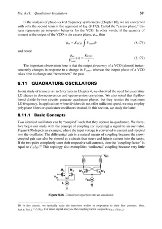
![582 Chap. 8. Oscillators
of the oscillator signal couples back to the input. By contrast, if implemented by, say, two
capacitors tied between Vin and the oscillator nodes, the coupling is bilateral.
Let us now consider two identical oscillators that are unilaterally coupled. Shown in
Fig. 8.97 are two possibilities, with “in-phase” and “anti-phase” coupling. The coupling
factors have the same sign in the former and opposite signs in the latter. We analyze these
topologies using both the feedback model and the one-port model of the oscillators. Note
that the tuning techniques described earlier in this chapter apply to these topologies as well.
(a) (b)
Figure 8.97 In-phase and anti-phase coupling of two oscillators.
Feedback Model The circuits of Fig. 8.97 can be mapped to two coupled feedback oscil-
lators as shown in Fig. 8.98, where |α1| 5 |α2| and the sign of α1α2 determines in-phase or
anti-phase coupling [18]. The output of the top adder is equal to α1Y 2 X, yielding
X 5 (α1Y 2 X)H(s). (8.178)
H ( )
s
H ( )
s Y
α2
α
X
1
Figure 8.98 Feedback model of quadrature oscillator.](https://image.slidesharecdn.com/rfmicroelectronicsrazavi-230814101614-71259b59/85/RF-MICROELECTRONICS_Razavi-pdf-607-320.jpg)
![Sec. 8.11. Quadrature Oscillators 583
Similarly, the bottom oscillator produces
Y 5 (α2X 2 Y)H(s). (8.179)
Multiplying both sides of (8.178) by α2X and both sides of (8.179) by α1Y and subtracting
the results, we have
α2X2
2 α1Y2
[1 1 H(s)] 5 0. (8.180)
As explained below, 1 1 H(s) 5 0 at the oscillation frequency, and hence
α2X2
5 α1Y2
. (8.181)
If α1 5 α2 (in-phase coupling), then X 5 ±Y, i.e., the two oscillators operate with a zero or
1808 phase difference.
Example 8.44
Applying Barkhausen’s criteria, explain why 1 1 H(s) 5 0 at the oscillation frequency if
α1 5 α2.
Solution:
Since each oscillator receives an additional input from the other, the oscillation startup
condition must be revisited. Drawing one half of the circuit as shown in Fig. 8.99(a), we
note that the input path can be merged with the feedback path as illustrated in Fig. 8.99(b).
The equivalent loop transmission is therefore equal to 2(1 ± α1)H(s), which, according to
Barkhausen, must be equal to unity:
2 (1 ± α1)H(s 5 jω0) 5 1. (8.182)
That is,
H( jω0) 5
21
1 ± α1
. (8.183)
This equation serves as the startup condition.
H ( )
s
Y
α
X
1 = X
+
−
X
+
−α1 H ( )
s X
+
−α1
1
(a) (b)
Figure 8.99 (a) Simplified model of coupled oscillators, (b) equivalent system.](https://image.slidesharecdn.com/rfmicroelectronicsrazavi-230814101614-71259b59/85/RF-MICROELECTRONICS_Razavi-pdf-608-320.jpg)
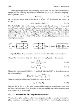
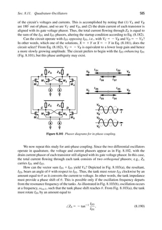
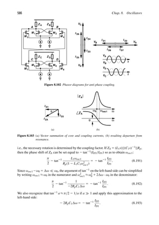
![Sec. 8.11. Quadrature Oscillators 587
Since 2RpC1ω0 5 2Qtank,
ω 5
ω0
2Qtank
tan21 ID3
ID1
. (8.194)
Equation (8.95) yields the same result.
Example 8.45
In the phasor diagram of Fig. 8.102, we have assumed that VC is 908 ahead of VA. Is it
possible for VC to remain 908 behind VA?
Solution:
Yes, it is. We construct the phasor diagram as shown in Fig. 8.104(a), noting that ID3
now points upward. Depicted in Fig. 8.104(b), the resultant of ID1 and ID3 must now be
rotated counterclockwise by the tank, requiring that the oscillation frequency fall below ω0
[Fig. 8.104(c)]. In this c](https://image.slidesharecdn.com/rfmicroelectronicsrazavi-230814101614-71259b59/85/RF-MICROELECTRONICS_Razavi-pdf-612-320.jpg)
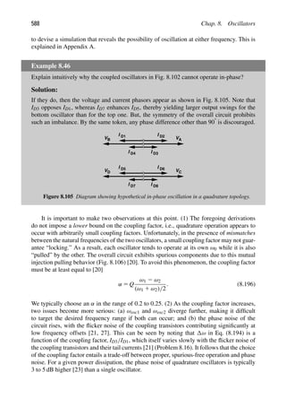
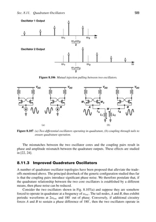
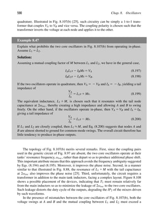
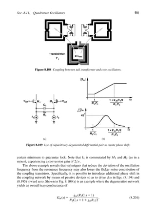
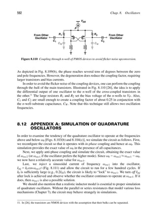
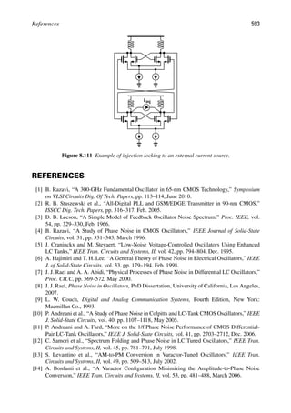
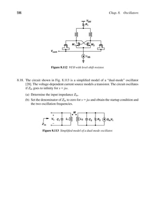
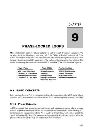
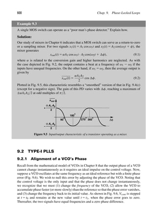
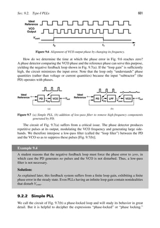
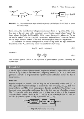
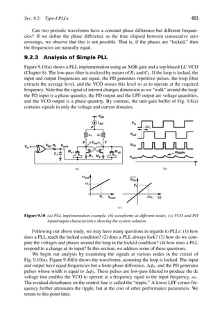
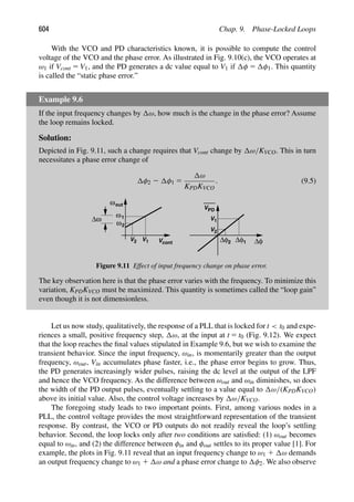
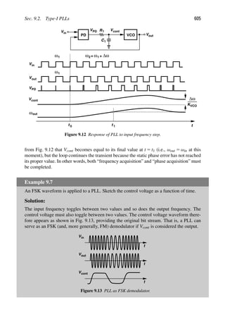
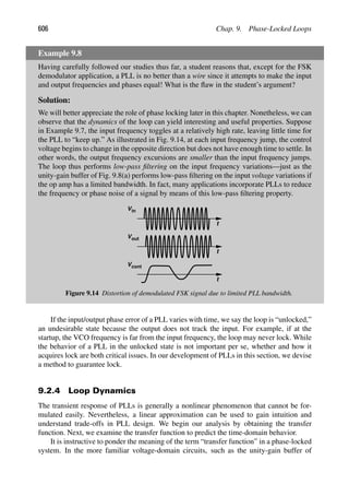
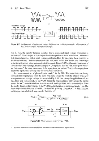
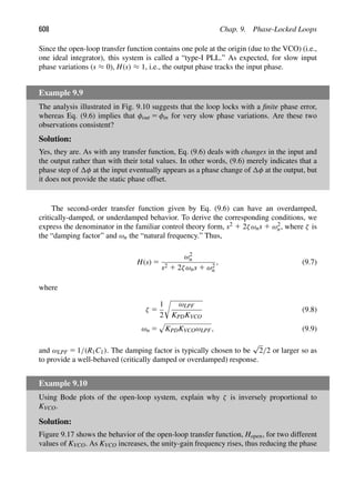
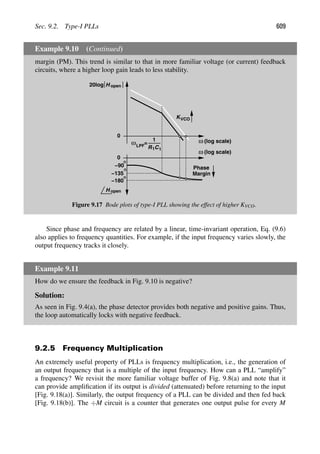
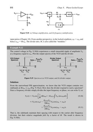
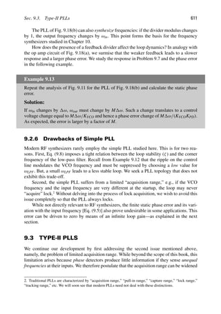
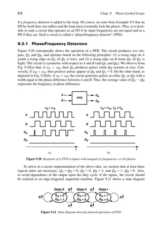
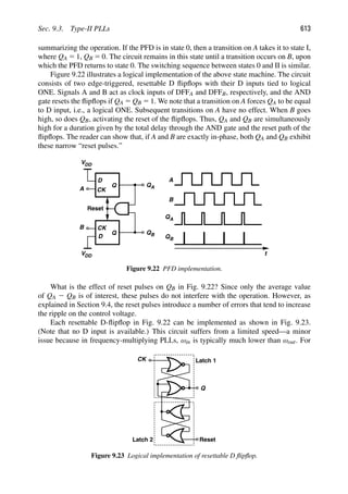
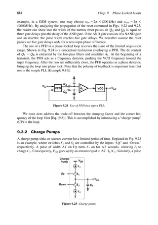
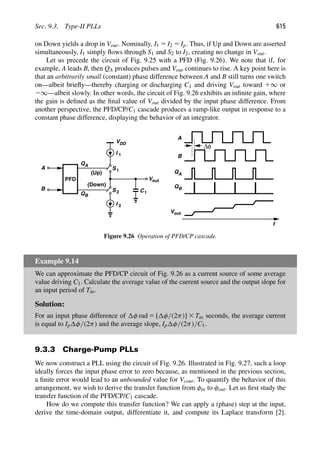
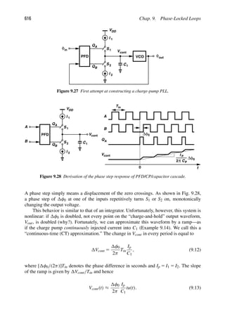
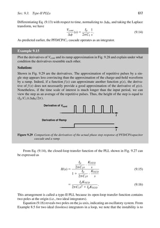
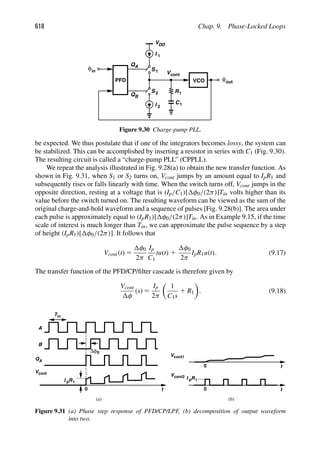
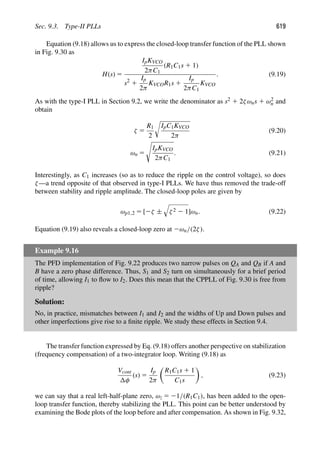
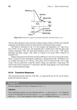
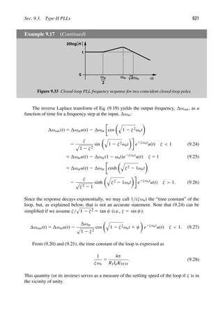
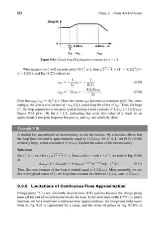
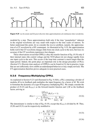
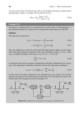
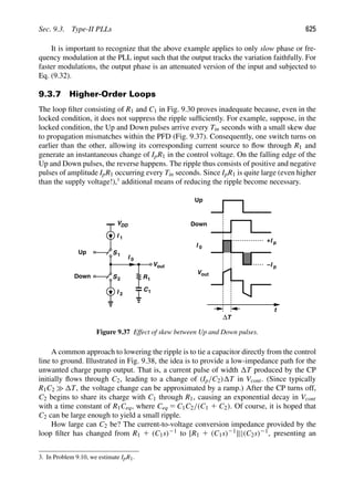
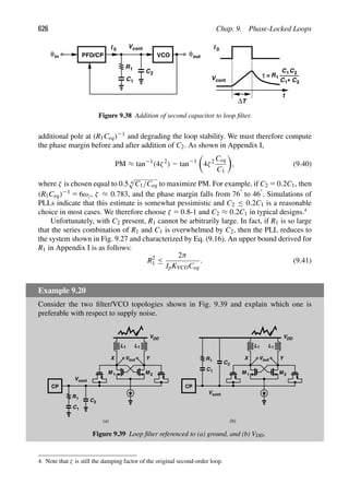
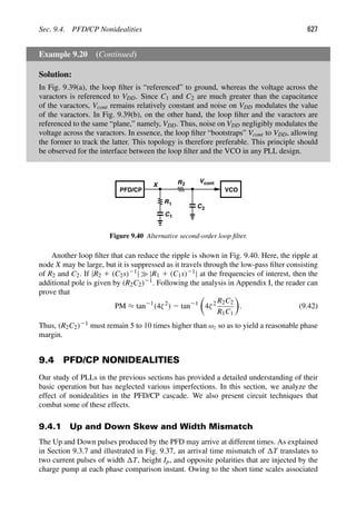
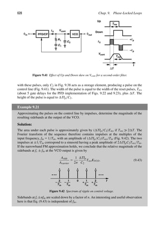
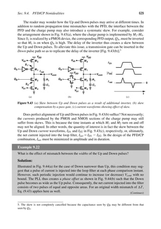
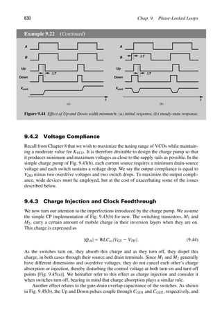
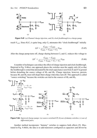
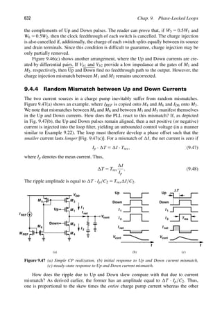
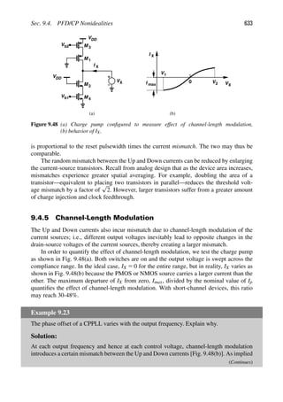
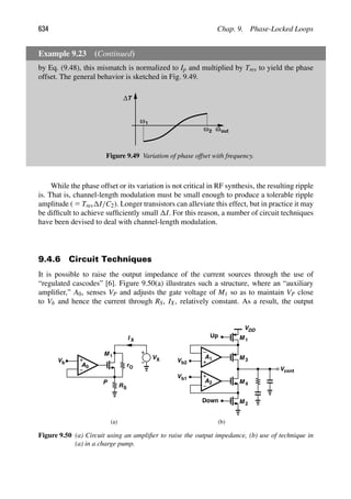
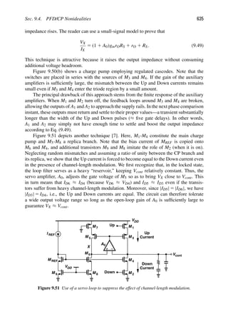
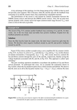
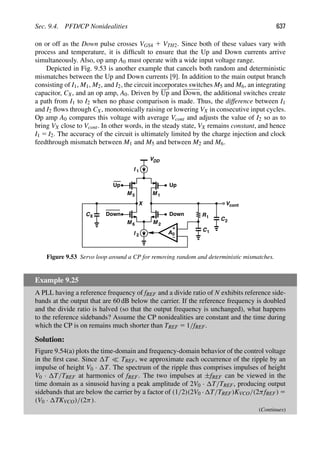
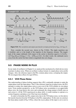
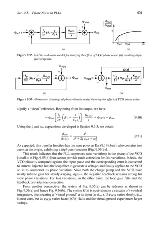
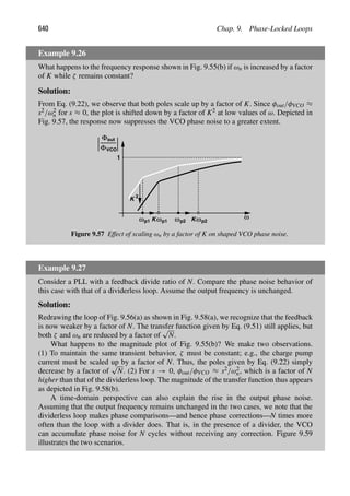
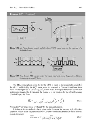
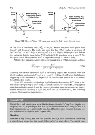
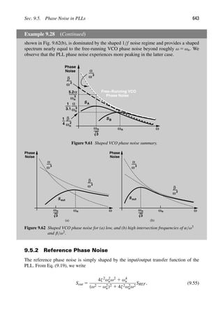
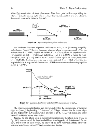
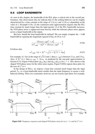
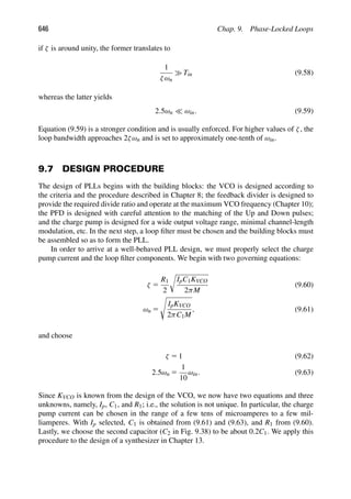
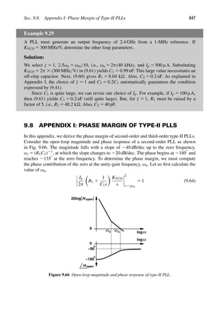

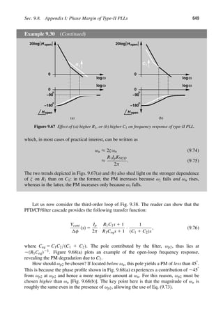
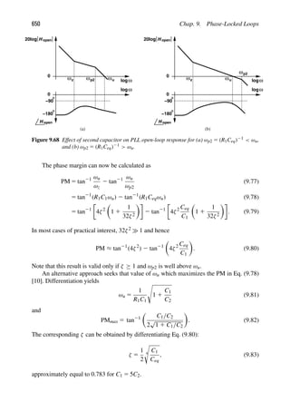
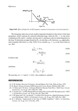
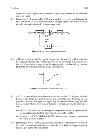
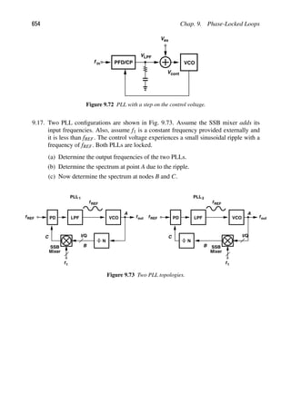
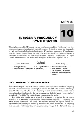
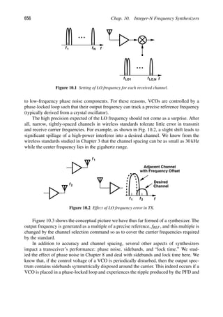
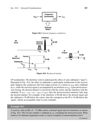
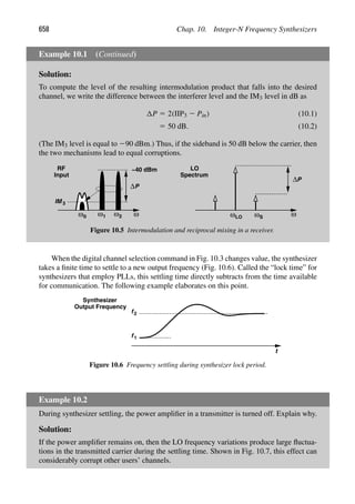
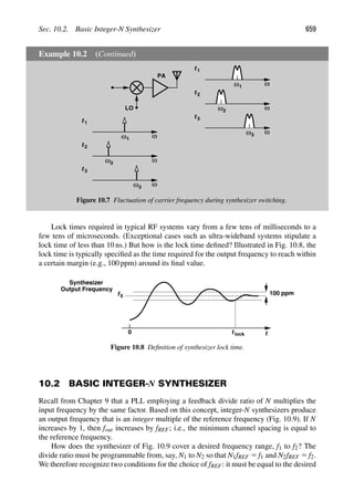
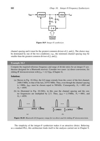
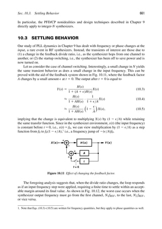
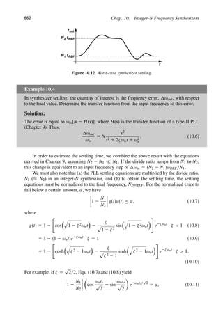
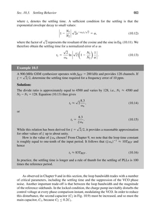
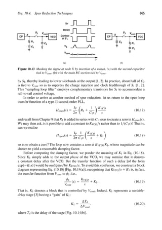
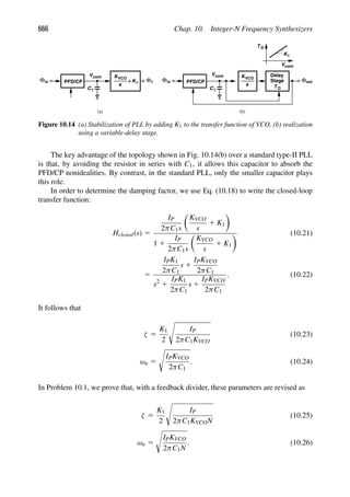
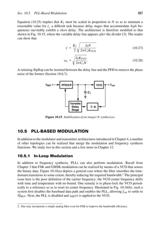
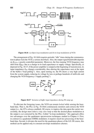
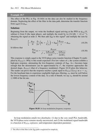
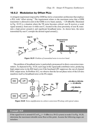
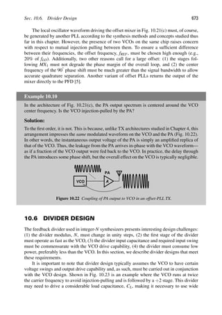
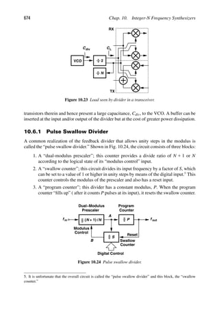
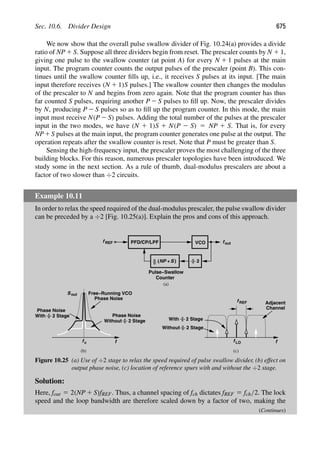
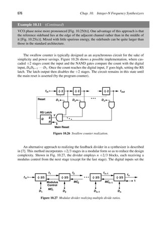
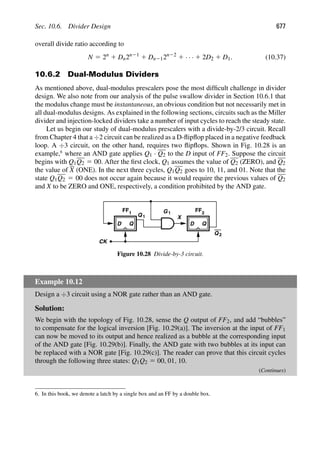
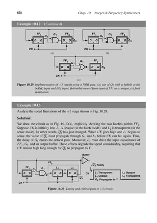
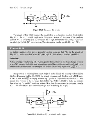
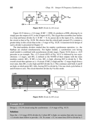
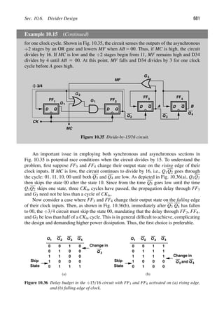
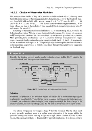
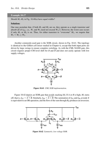
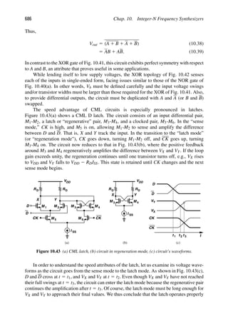
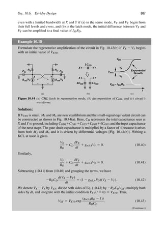
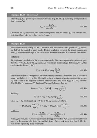
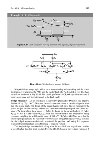
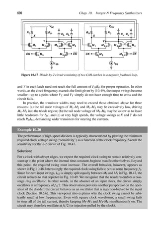
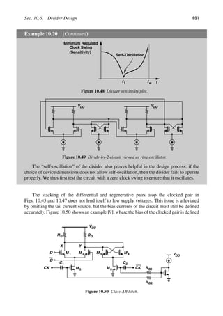
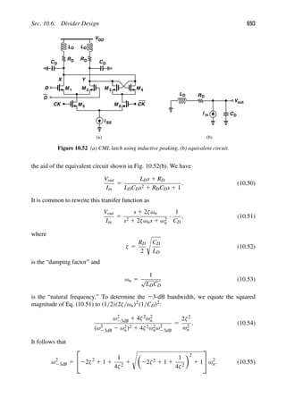
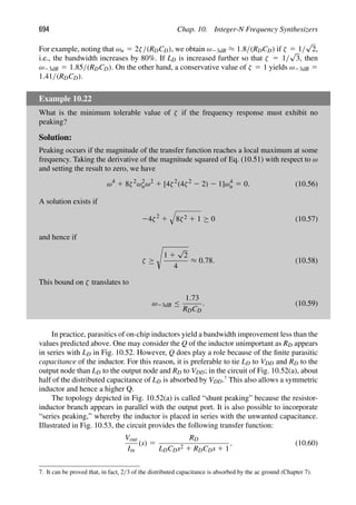
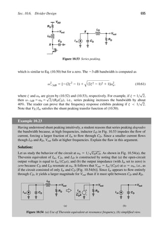
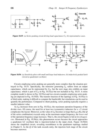
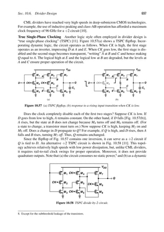
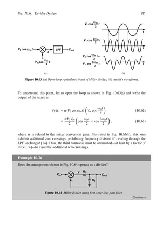
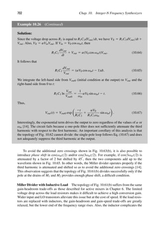
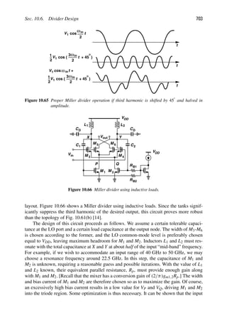
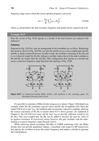
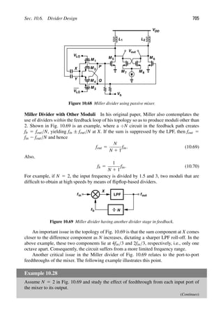
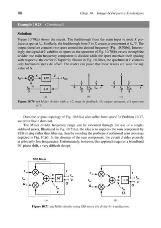
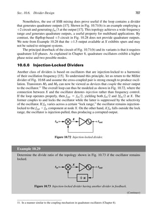
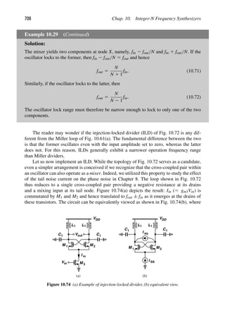
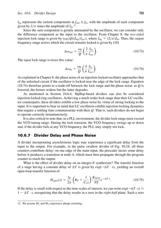
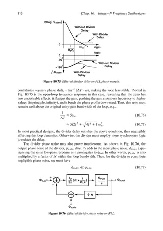

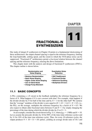
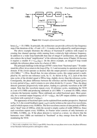
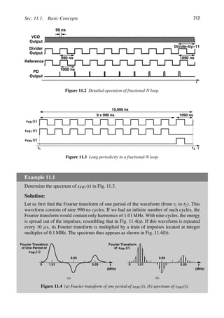
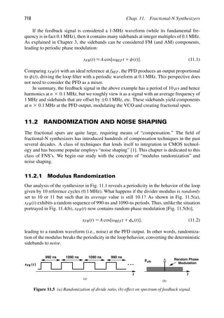
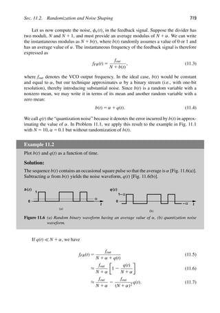
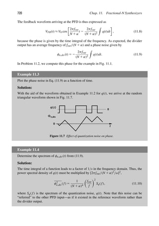
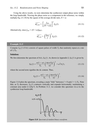
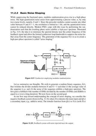
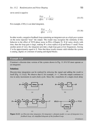
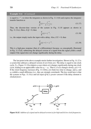
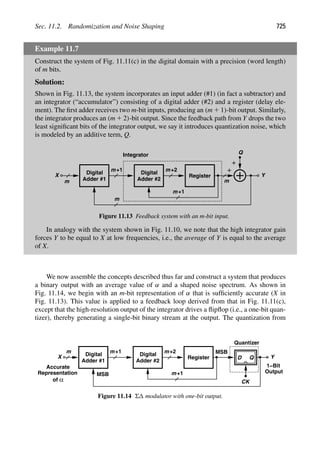
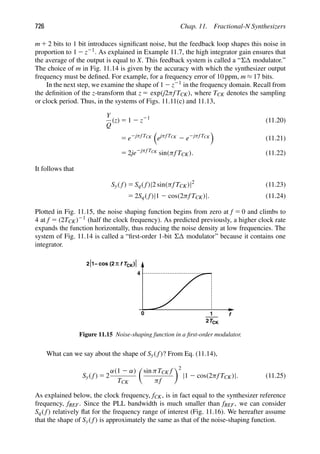
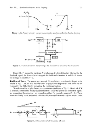
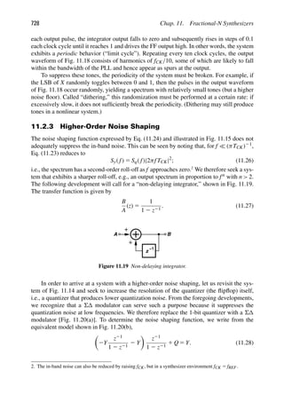
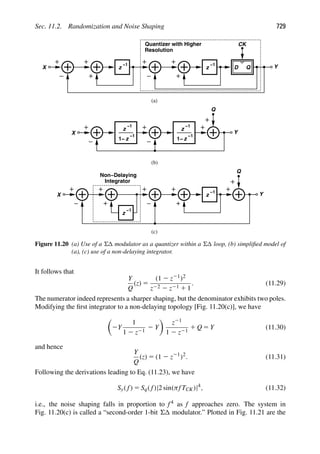
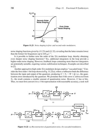
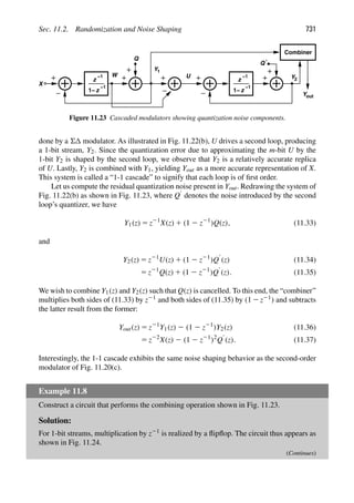
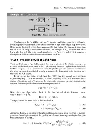
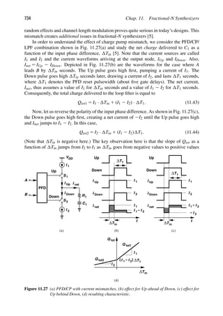
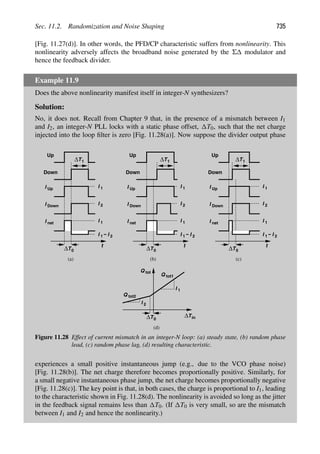
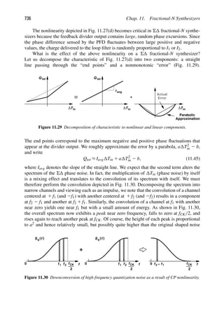
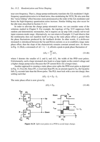
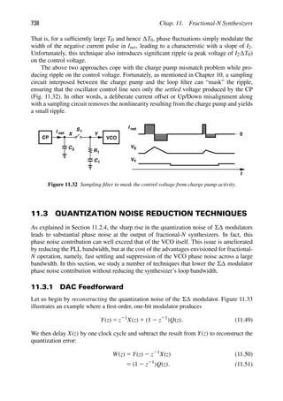
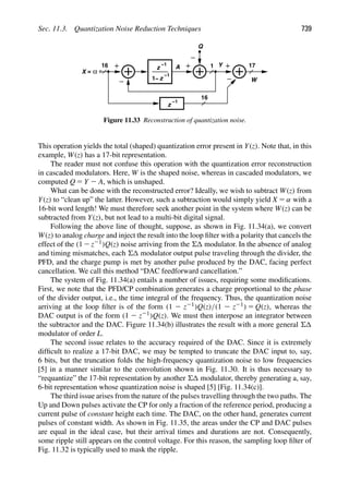
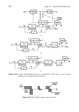
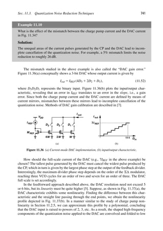
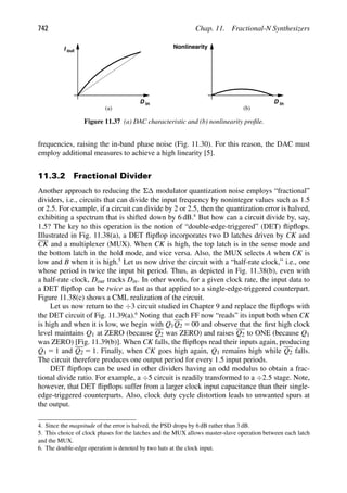
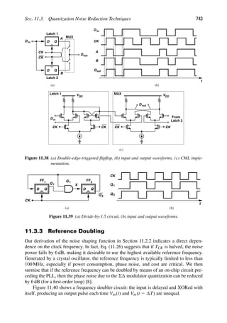
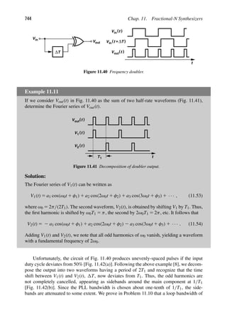
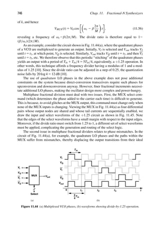
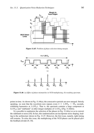
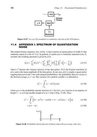

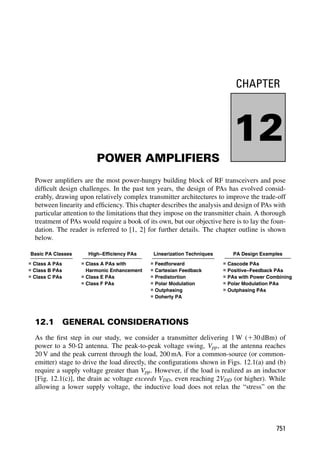
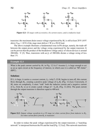
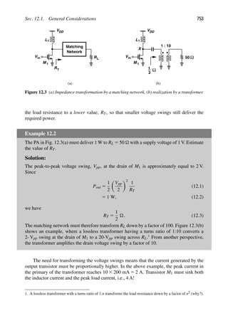
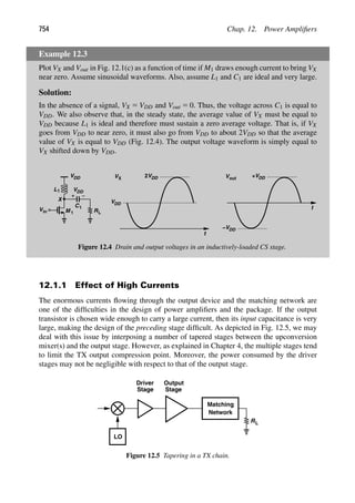
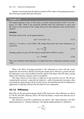
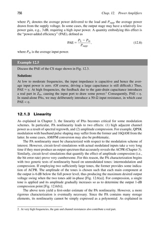
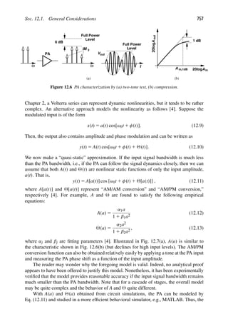
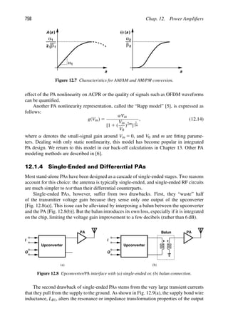
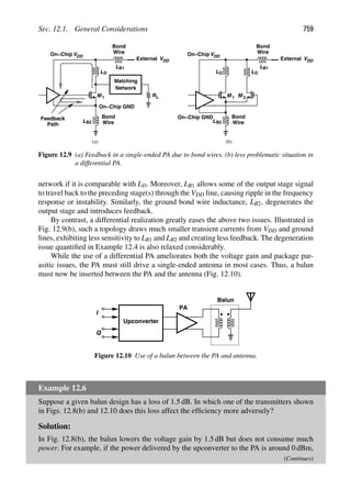
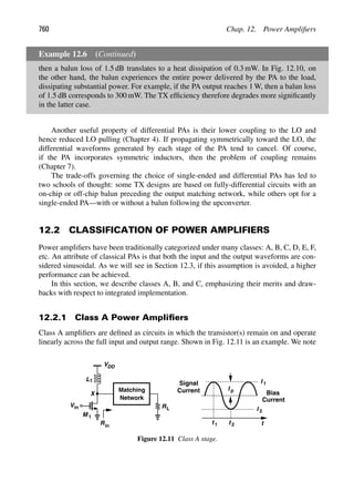
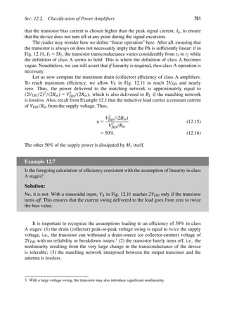
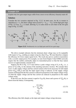
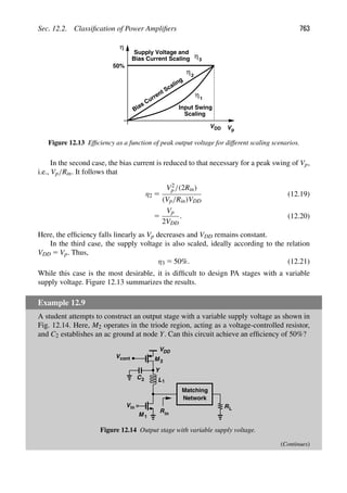
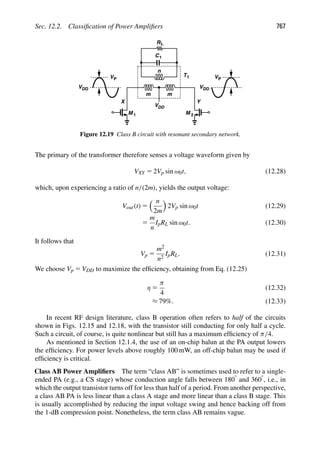
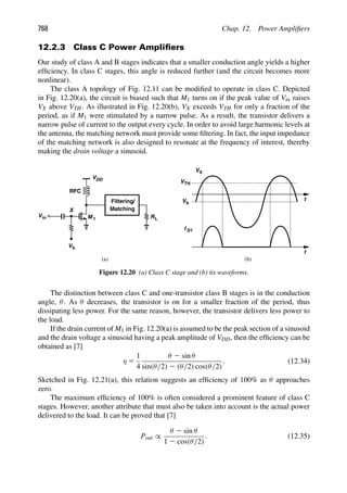
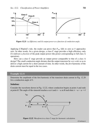
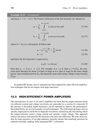
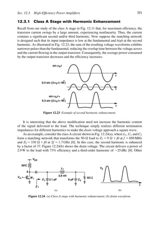
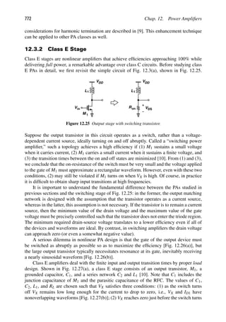
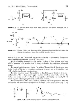
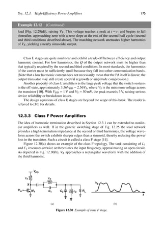
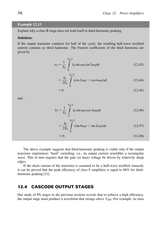
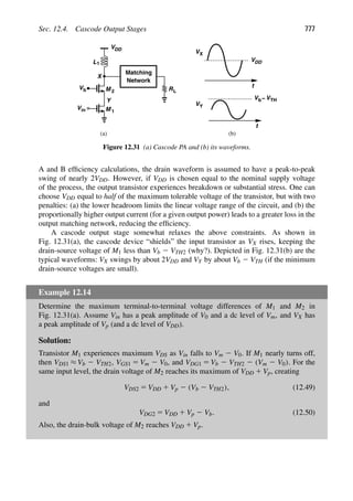
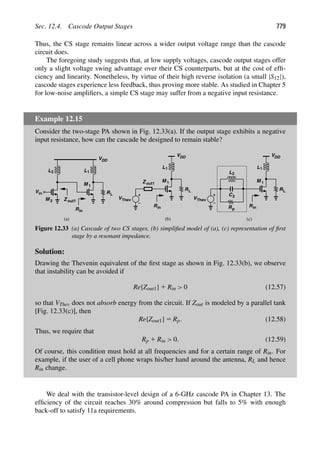
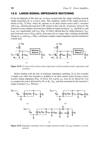
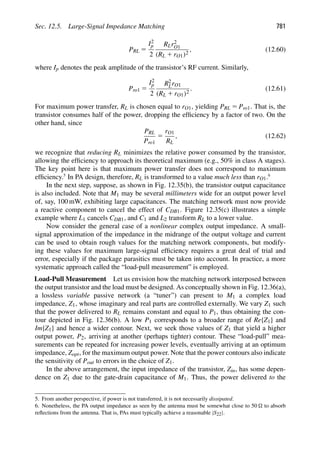
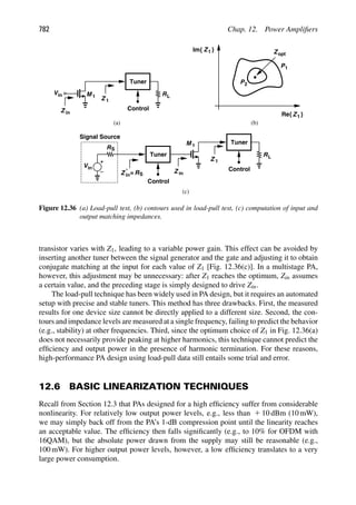
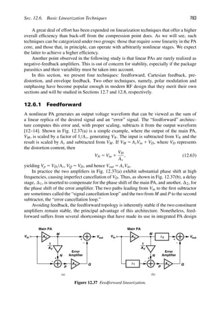
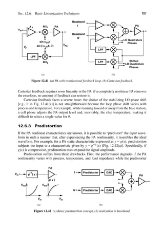
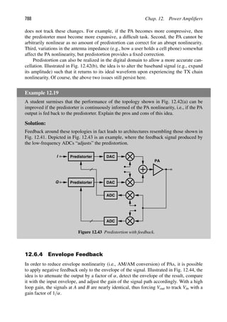
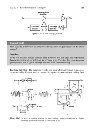
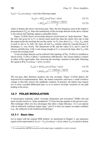
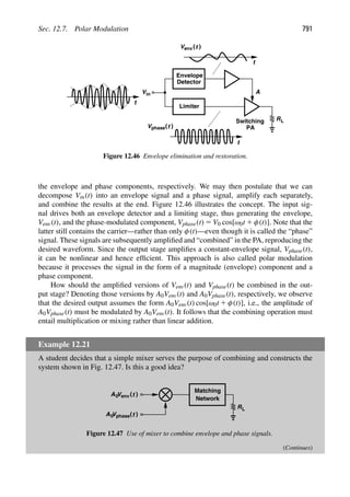
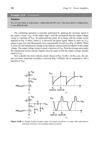
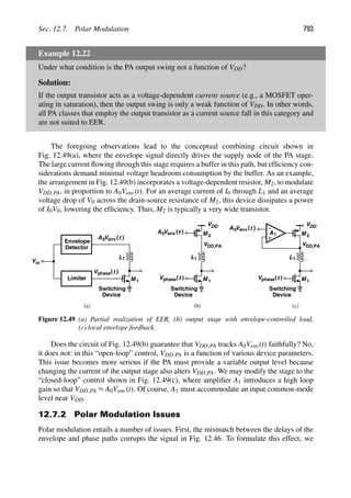
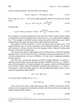
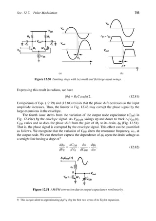
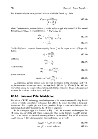
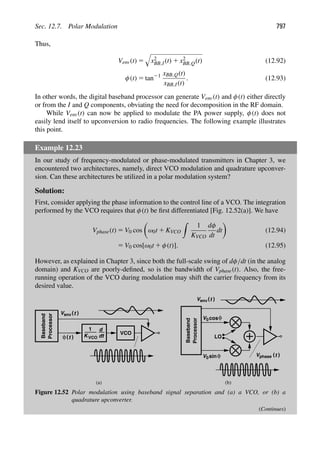
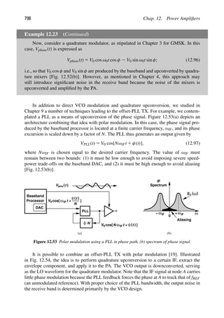
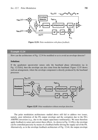
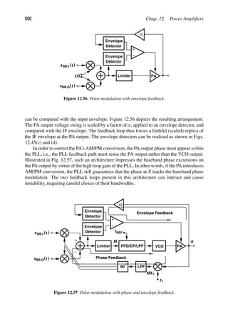
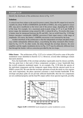
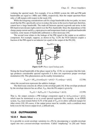
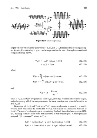
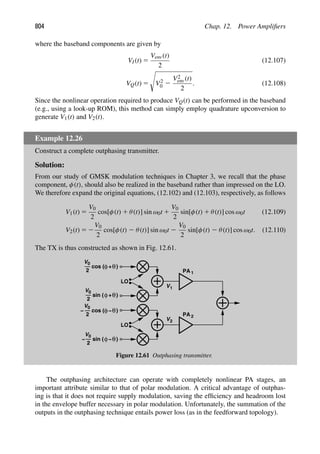
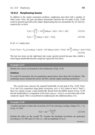
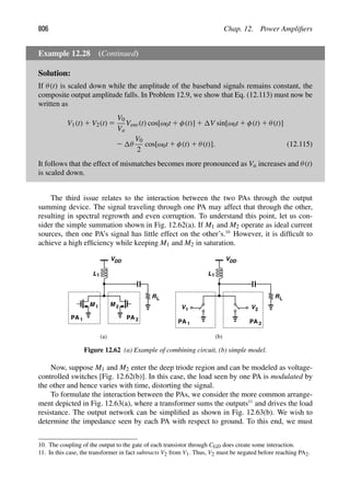
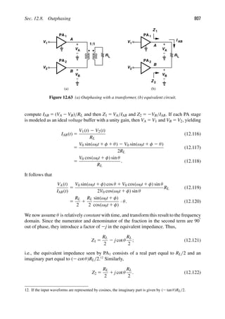
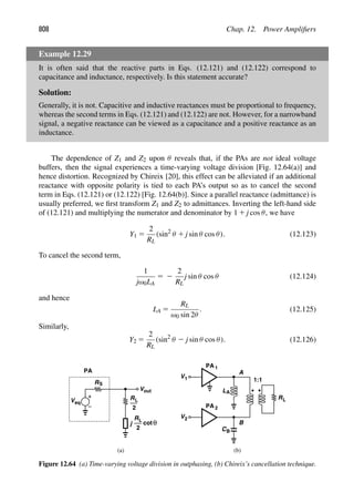
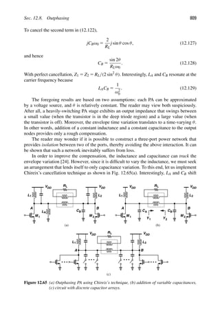
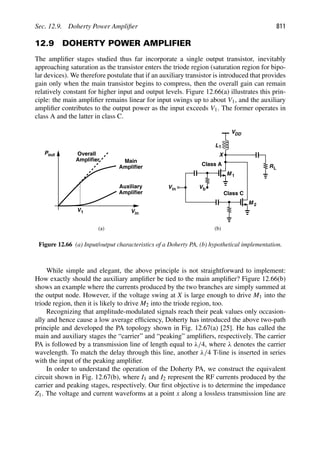
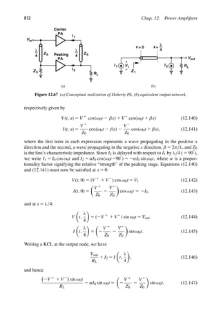
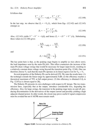
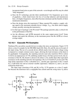
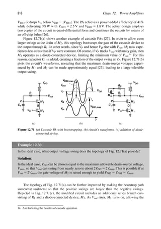
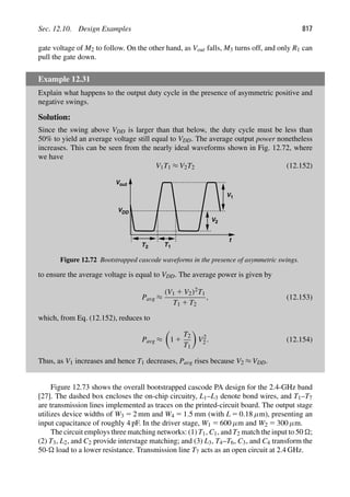
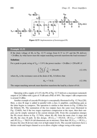
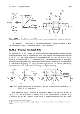
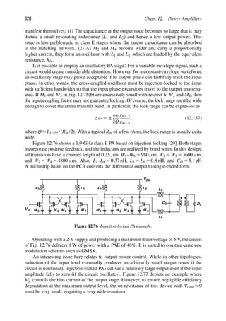
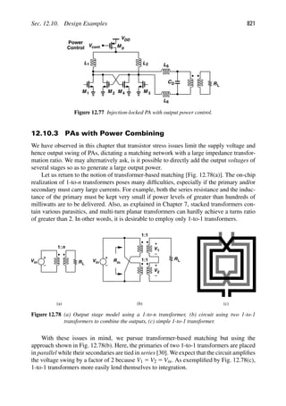
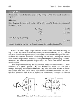
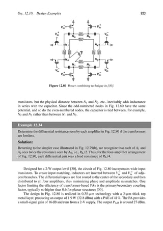
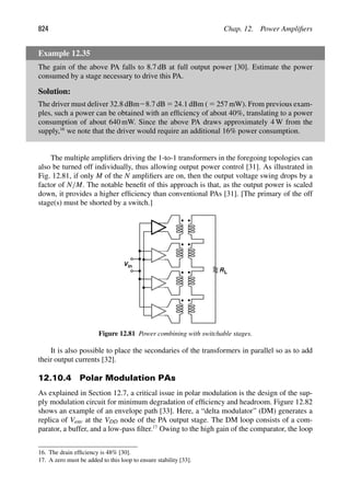
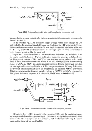
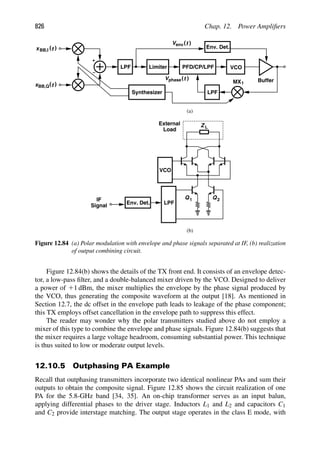
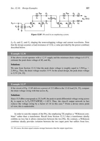


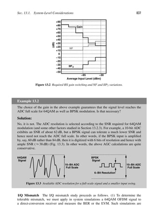
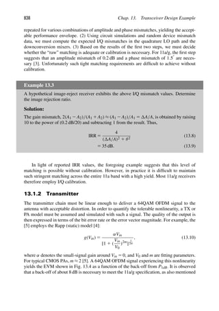
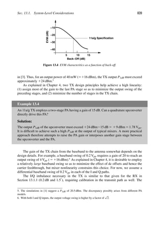
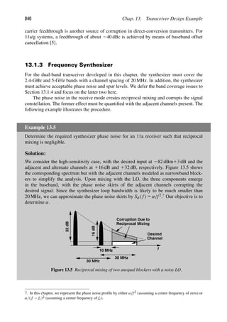
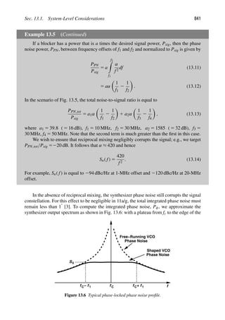
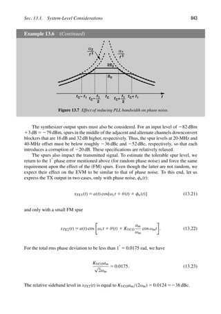
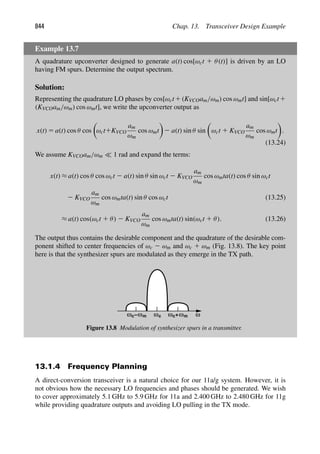
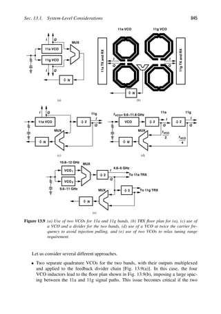
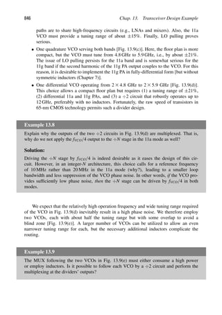
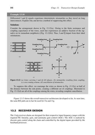
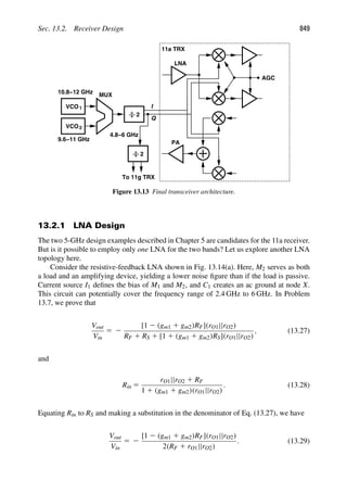
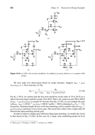
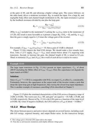
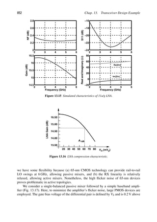
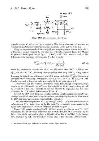
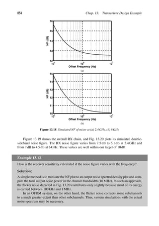
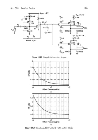
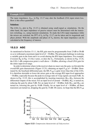
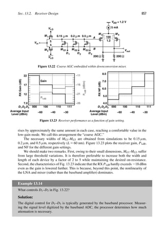
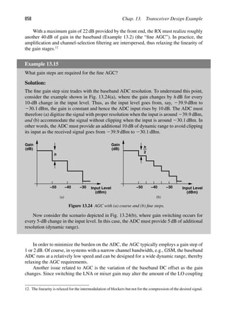
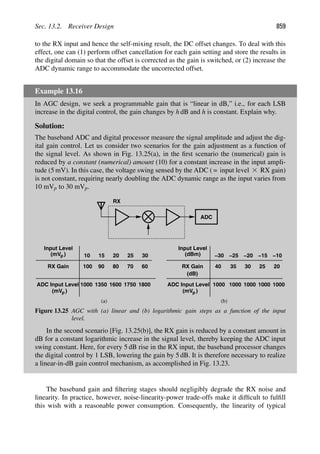
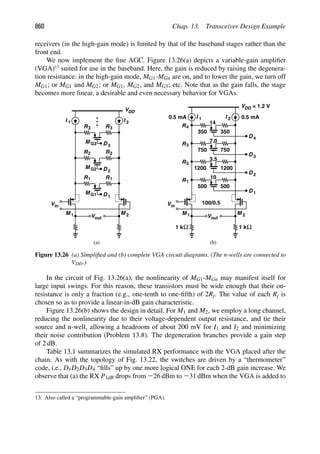
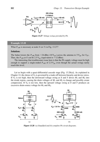
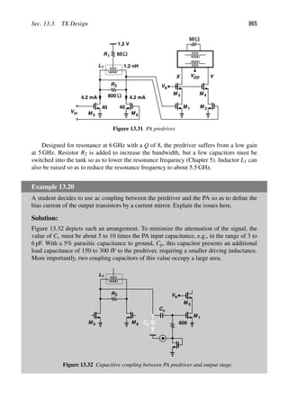
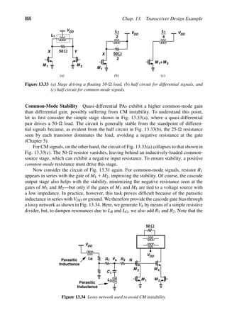
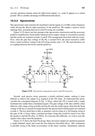
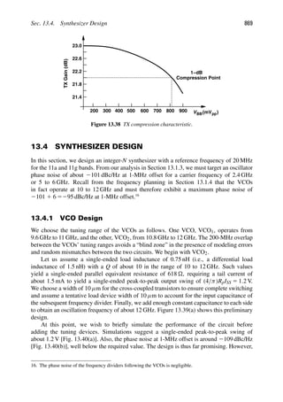
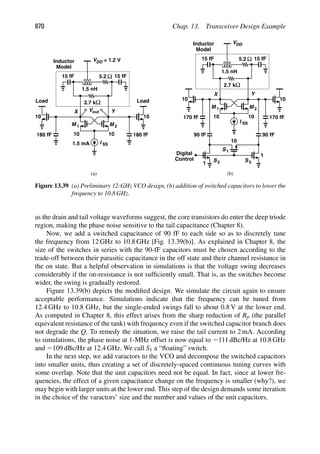
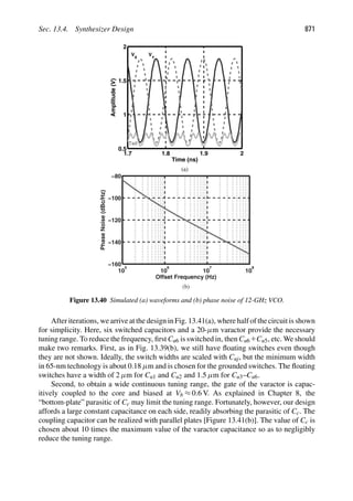
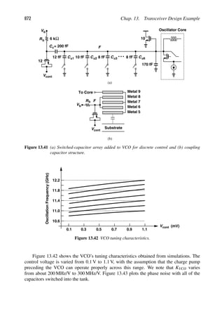
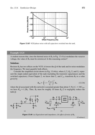
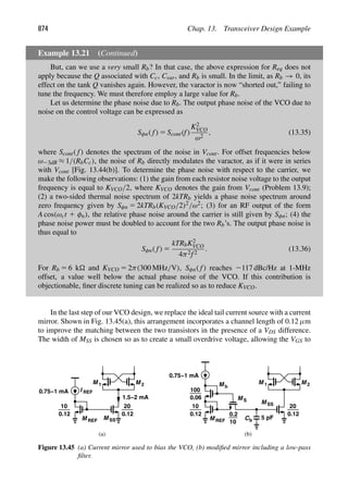
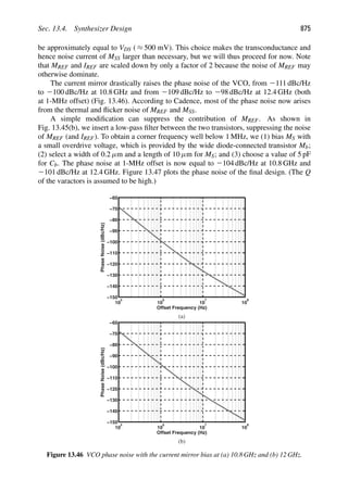
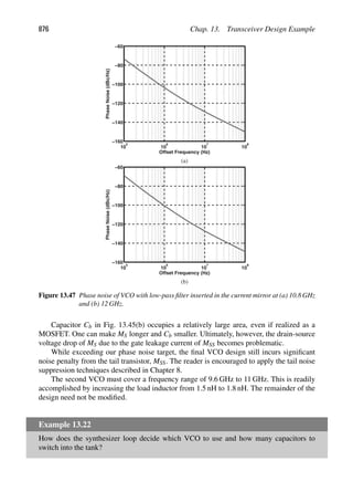
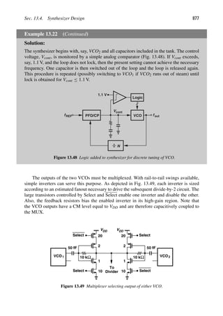
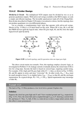
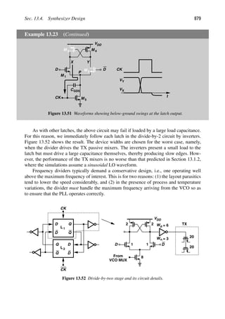
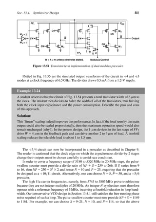
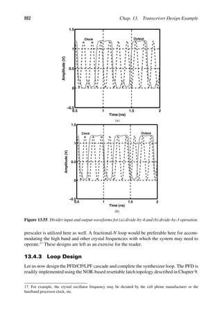
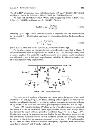
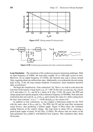
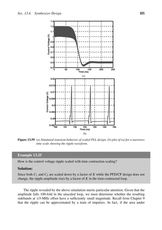
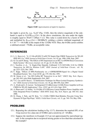


![RF Circuit Design - [Ch1-2] Transmission Line Theory](https://cdn.slidesharecdn.com/ss_thumbnails/ch1-2-150613064349-lva1-app6892-thumbnail.jpg?width=640&height=640&fit=bounds)


![Multiband Transceivers - [Chapter 6] Multi-mode and Multi-band Transceivers](https://cdn.slidesharecdn.com/ss_thumbnails/ch6-150613070935-lva1-app6891-thumbnail.jpg?width=640&height=640&fit=bounds)