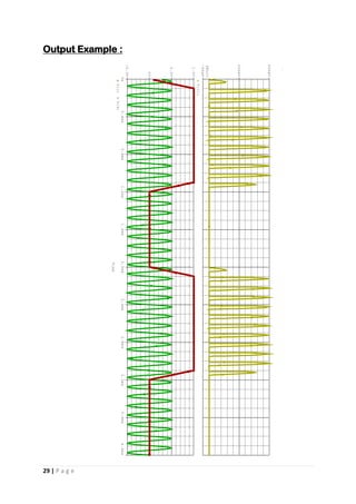
Downloaded 16 times
![20 | P a g e
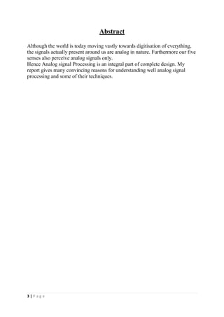
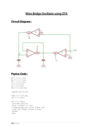
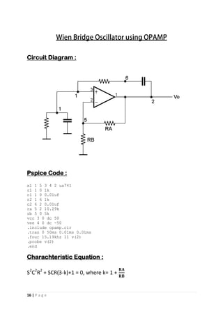
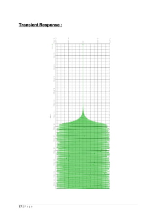
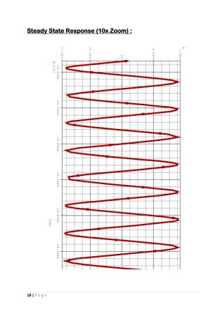
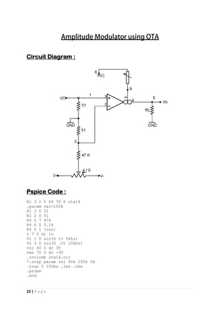
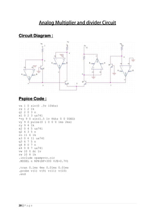
Circuit Diagram :
Pspice Code :
x1 1 3 5 6 4 2 AD844/AD
.param val=2.64k
.param vall=1uf
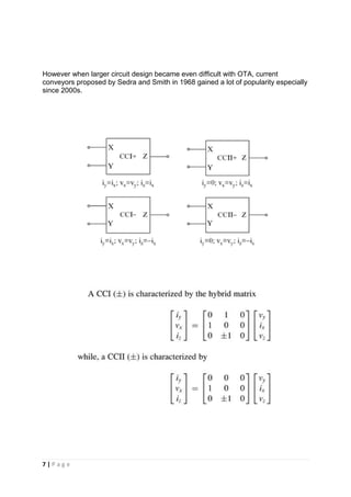
r3 1 0 {val}
c6 1 2 {vall} ic=1ua
*r10 1 2 11k
r4 3 0 1k
c 2 0 .8uf ic=1ua
*r11 2 0 11k
r2 3 4 1k
vcc 5 0 dc 10v
vee 6 0 dc -10v
.tran 30ms 250ms 0.01ms 0.01ms uic
*.step param vall .79uf .81uf 0.001uf
.probe v(4)
.four 0.109khz 11 v(4)
.include cfoa.cir
.end
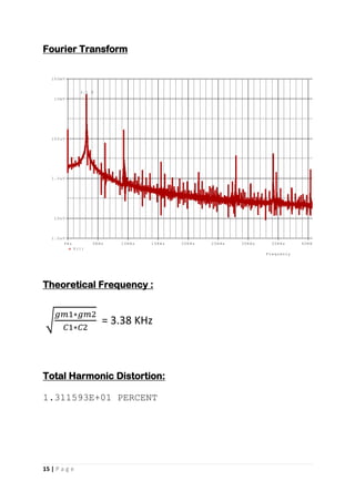
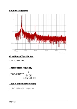
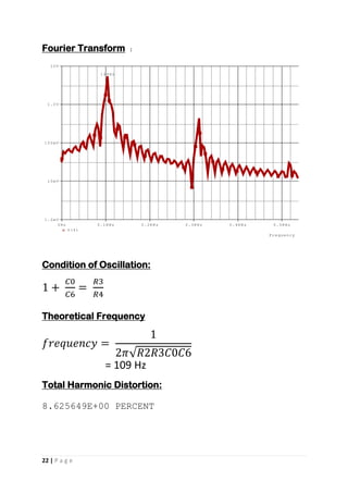
Charachteristic Equation :
S2
[R2R3R4C0C6] + S[-R2R3C6+R2R4C0+C6R2R4] + R4 = 0](https://image.slidesharecdn.com/1796624a-078e-4de8-b1da-2bc50ddd73cc-150810165409-lva1-app6892/85/ASP-20-320.jpg)
![26 | P a g e
History and Background
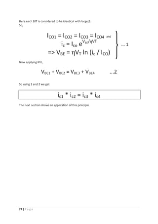
A translinear circuit is a circuit that carries out its function using the translinear principle.
These are current-mode circuits that can be made using transistors that obey
anexponential current-voltage characteristic—this includes BJTs and CMOS transistors in
weak inversion.
The word translinear (TL) was invented by Barrie Gilbert in 1975[1] to describe circuits that
used the exponential current-voltage relation of BJTs.[2][3] By using this exponential
relationship, this class of circuits can implement multiplication, amplification and power-law
relationships. When Barrie Gilbert described this class of circuits he also described the
translinear principle (TLP) which made the analysis of these circuits possible in a way that
the simplified view of BJTs as linear current amplifiers did not allow. TLP was later extended
to include other elements that obey an exponential current-voltage relationship (such as
CMOS transistors in weak inversion).
Usage in electronics today
The TLP has been used in a variety of circuits including vector arithmetic circuits,[6] current
conveyors, current-mode operational amplifiers, and RMS-DC converters.[7] It has been in
use since the 1960s (by Gilbert), but was not formalized until 1975.[1] In the 1980s, Evert
Seevinck's work helped to create a systematic process for translinear circuit design. In 1990
Seevinck invented a circuit he called a companding current-mode integrator[8] that was
effectively a first-order log-domain filter. A version of this was generalized in 1993 by
Douglas Frey and the connection between this class of filters and TL circuits was made most
explicit in the late 90s work of Jan Mulder et al. where they describe thedynamic translinear
principle. More work by Seevinck led to synthesis techniques for extremely low-power TL
circuits.[9] More recent work in the field has led to the voltage-translinear principle,
multiple-input translinear element networks, and field-programmable analog
arrays (FPAAs).
Principle](https://image.slidesharecdn.com/1796624a-078e-4de8-b1da-2bc50ddd73cc-150810165409-lva1-app6892/85/ASP-26-320.jpg)
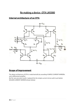

This document appears to be a student project report on analog signal processing. It includes an introduction discussing why analog signal processing is still important despite digitization trends. It then discusses some common issues with using operational amplifiers in analog circuits and advantages of using operational transconductance amplifiers instead. The report goes on to provide circuit diagrams and simulations of various analog filters and oscillators designed using OTAs.


![RF Module Design - [Chapter 8] Phase-Locked Loops](https://cdn.slidesharecdn.com/ss_thumbnails/rfch8-150613070348-lva1-app6892-thumbnail.jpg?width=640&height=640&fit=bounds)