This document discusses angle modulation techniques, specifically frequency modulation (FM) and phase modulation (PM). It defines these terms and discusses the key aspects of narrowband and wideband FM. Narrowband FM has a modulation index below 1, while wideband FM is above 0.5. Carson's rule provides an estimate for the bandwidth of an FM signal. FM can be demodulated using a frequency discriminator or phase-locked loop (PLL). The PLL performs better in noise. Wideband FM transmission is used for broadcast to transmit high quality audio over a large bandwidth.

![EC8491: Communication Theory Department of ECE
With a tone-modulated FM wave, if the modulation frequency is held constant and the modulation
index is increased, the (non-negligible) bandwidth of the FM signal increases but the spacing between
spectra remains the same; some spectral components decrease in strength as others increase. If the
frequency deviation is held constant and the modulation frequency increased, the spacing between
spectra increases.
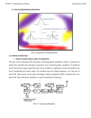
Frequency modulation can be classified as narrowband if the change in the carrier frequency is
about the same as the signal frequency, or as wideband if the change in the carrier frequency is
much higher (modulation index >1) than the signal frequency. [6]
For example, narrowband FM is
used for two way radio systems such as Family Radio Service, in which the carrier is allowed to
deviate only 2.5 kHz above and below the center frequency with speech signals of no more than
3.5 kHz bandwidth. Wideband FM is used for FM broadcasting, in which music and speech are
transmitted with up to 75 kHz deviation from the center frequency and carry audio with up to a 20-
kHz bandwidth.
Carson's rule:
BT = 2∆f + fm.
2.2 NARROW BAND FMMODULATION:
NarrowbandFM: If the modulation index of FM is kept under 1, then the FM produced is
regarded as narrow bandFM.
Thecasewhere|θm(t)|≪1foralltiscalled narrow band FM. Using the approximations
cosx≃1andsinx ≃x for|x|≪1,theFMsignalcanbeapproximatedas:
s(t) = Ac cos[ωct + θm(t)]
= Ac cos ωct cos θm(t) − Ac sin ωctsinθm(t)
≃ Ac cos ωct–Acθm(t) sin ωct
or in complex notation
st= ACRE{ejwct
(1 + jθmt}
ThisissimilartotheAMsignalexceptthatthediscretecarriercomponentAccoswc(t)is90°out of phase
with the sinusoid Ac sinwc(t) multiplying the phase angle θm(t). The spectrum of narrow band
FM is similar to that ofAM.
The Bandwidth of an FMSignal:
The following formula, known as Carson‘s rule is often used as an estimate of the FM signal](https://image.slidesharecdn.com/ct-2-240205042339-b6e34c0e/85/Communication-Theory-Angle-Modulation-pdf-4-320.jpg)
![EC8491: Communication Theory Department of ECE
=
st
bandwidth: BT = 2(∆f + fm) Hz
where∆f is the peak frequency deviation and fm is the maximum baseband message
frequencycomponent.
FM Demodulation by a Frequency Discriminator:
A frequency discriminator is a device that converts a received FM signal into a voltage that is
proportional to the instantaneous frequency of its input without using a local oscillator and,
consequently, in a non coherentmanner.
• When the instantaneous frequency changes slowly relative to the time-constantsofthe filter, a
quasi-static analysis can beused.
• In quasi-static operation the filter output has the same instantaneous frequency as the input but
with an envelope that varies according to the amplitude response of the filter at the
instantaneousfrequency.
• Theamplitudevariationsarethendetectedwithanenvelopedetectorliketheonesused for
AMdemodulation.
An FM Discriminator Using the Pre-Envelope:
When θm(t) is small and band-limited so that cos θm(t) and sinθm(t) are essentially band-limited
signals with cut off frequencies less than fc, the pre-envelope of the FM signal is
s+(t) = s(t) + jˆs(t) = Acej
(ωct+θm(t)) The
angle of the pre-envelope is φ'(t) = arctan[ˆs(t)/s(t)] = ωct + θm(t) The
derivative of the phase is =ωct+ kθm(t)
t
d
dφt std sdt
−
= ωct + kωm (t)
dt dtst s2t+s^2(t)
which is exactly the instantaneous frequency. This can be approximated in discrete-time by
using FIR filters to form the derivatives and Hilbert transform. Notice that the denominator is
the squared envelope of the FM signal.
This formula can also be derived by observing,
d
st=
dt
d
ACcosωct + θmt= −ACωct + kωmtsin [ωct + θmt]
dt](https://image.slidesharecdn.com/ct-2-240205042339-b6e34c0e/85/Communication-Theory-Angle-Modulation-pdf-5-320.jpg)
![EC8491: Communication Theory Department of ECE
So,
d
s^t=
dt
d
ACsinωct + θmt= ACωct + kωmtcos [ωct + θmt]
dt
std
dts^(t) −
s^(t)d
=AC2
ωct+kωmt∗ cos2[wct+θmt+sin2[wct+θmt dtst
The bandwidth of an FM discriminator must be at least as great as that of the received FM
signal which is usually much greater than that of the baseband message. This limits the degree of
noise reduction that can be achieved by preceding the discriminator by a bandpass receive filter.
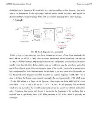
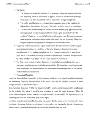
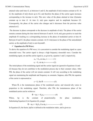
Using a Phase-Locked Loop for FMDemodulation:
A device called a phase-locked loop (PLL) can be used to demodulate an FM signal with better
performance in a noisy environment than a frequency discriminator. The block diagram of a
discrete-time version of a PLL as shown in figure,
FIG 2.2 PLL Block diagram
The block diagram of a basic PLL is shown in the figure below. It is basically a flip flop
consisting of a phase detector, a low pass filter (LPF),and a Voltage Controlled Oscillator (VCO)
The input signal Vi with an input frequency fi is passed through a phase detector. A phase detector
basically a comparator which compares the input frequency fiwith the feedback frequency fo .The
phase detector provides an output error voltage Ver (=fi+fo),which is a DC
voltage. This DC voltage is then passed on to an LPF. The LPF removes the high frequency noise
and produces a steady DC level, Vf (=Fi-Fo). Vf also represents the dynamic characteristics of the
PLL.
The DC level is then passed on to a VCO. The output frequency of the VCO (fo) is directly
proportional to the input signal. Both the input frequency and output frequency are compared and
adjusted through feedback loops until the output frequency equals the input frequency. Thus the
PLL works in these stages – free-running, capture and phase lock.](https://image.slidesharecdn.com/ct-2-240205042339-b6e34c0e/85/Communication-Theory-Angle-Modulation-pdf-6-320.jpg)