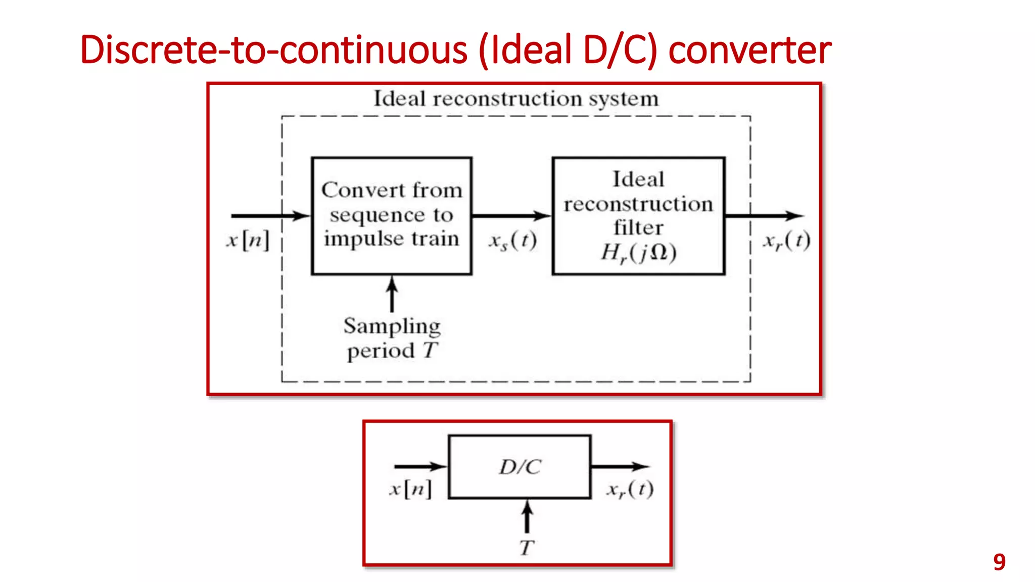
Download as PDF, PPTX

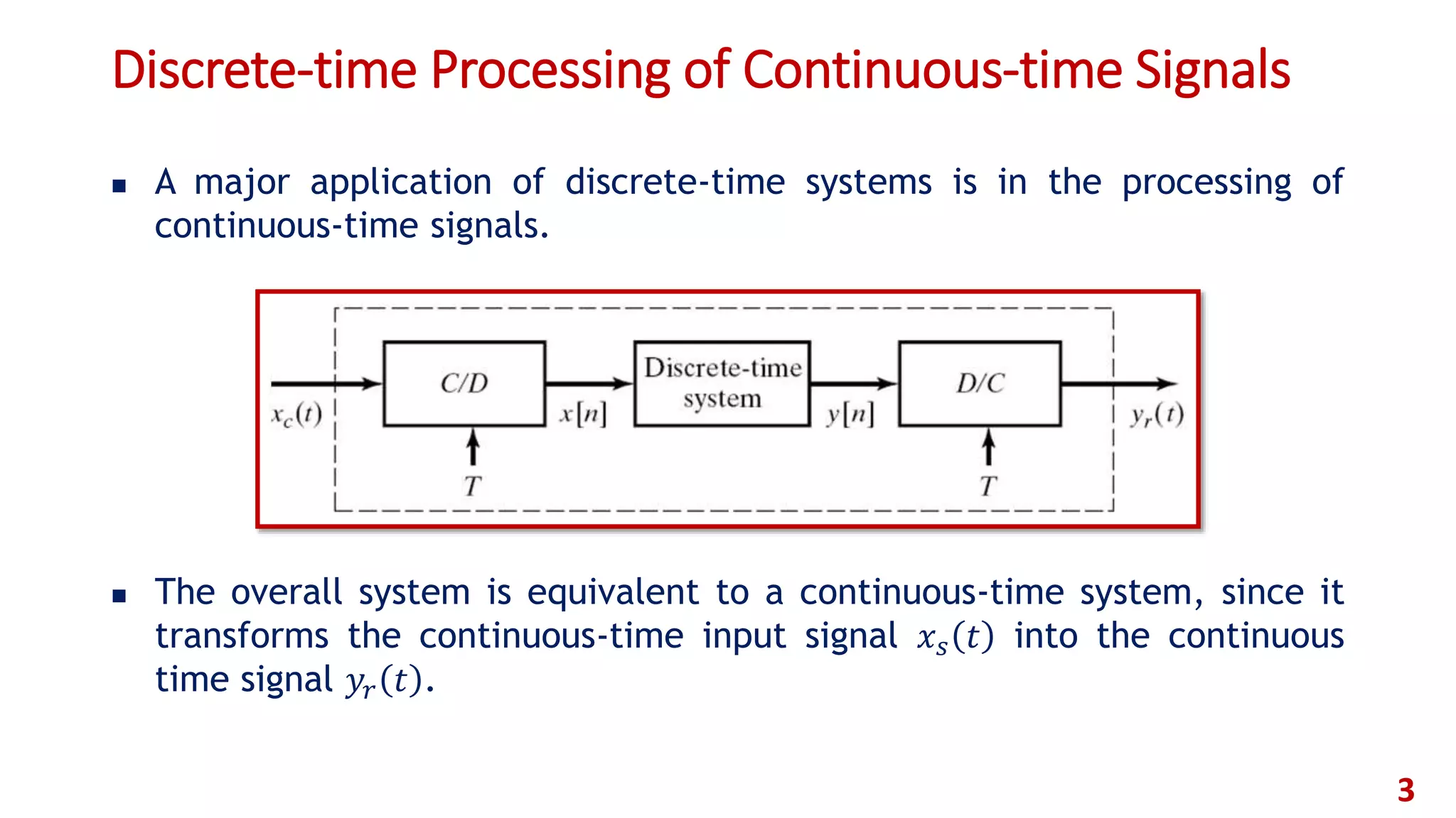
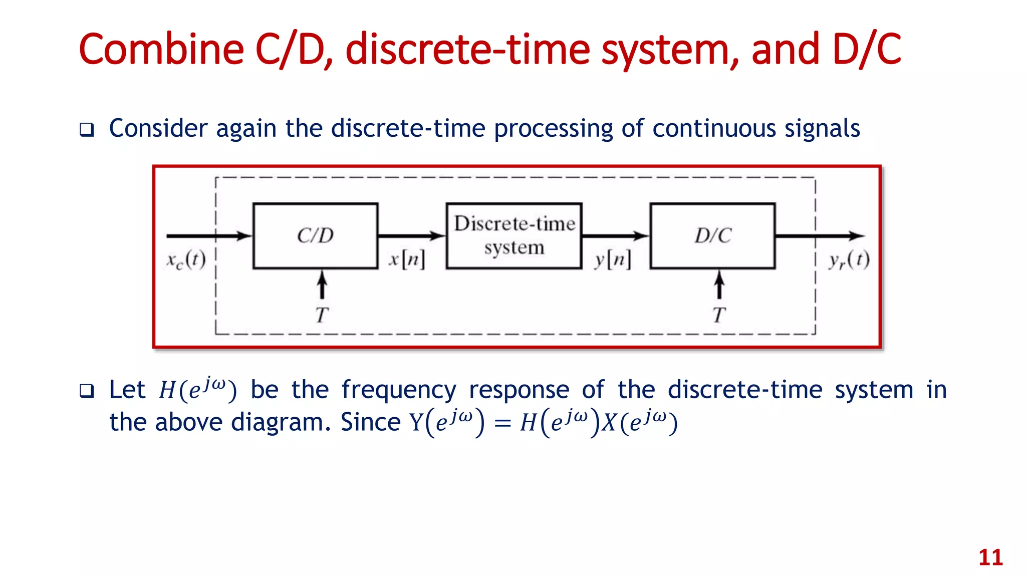
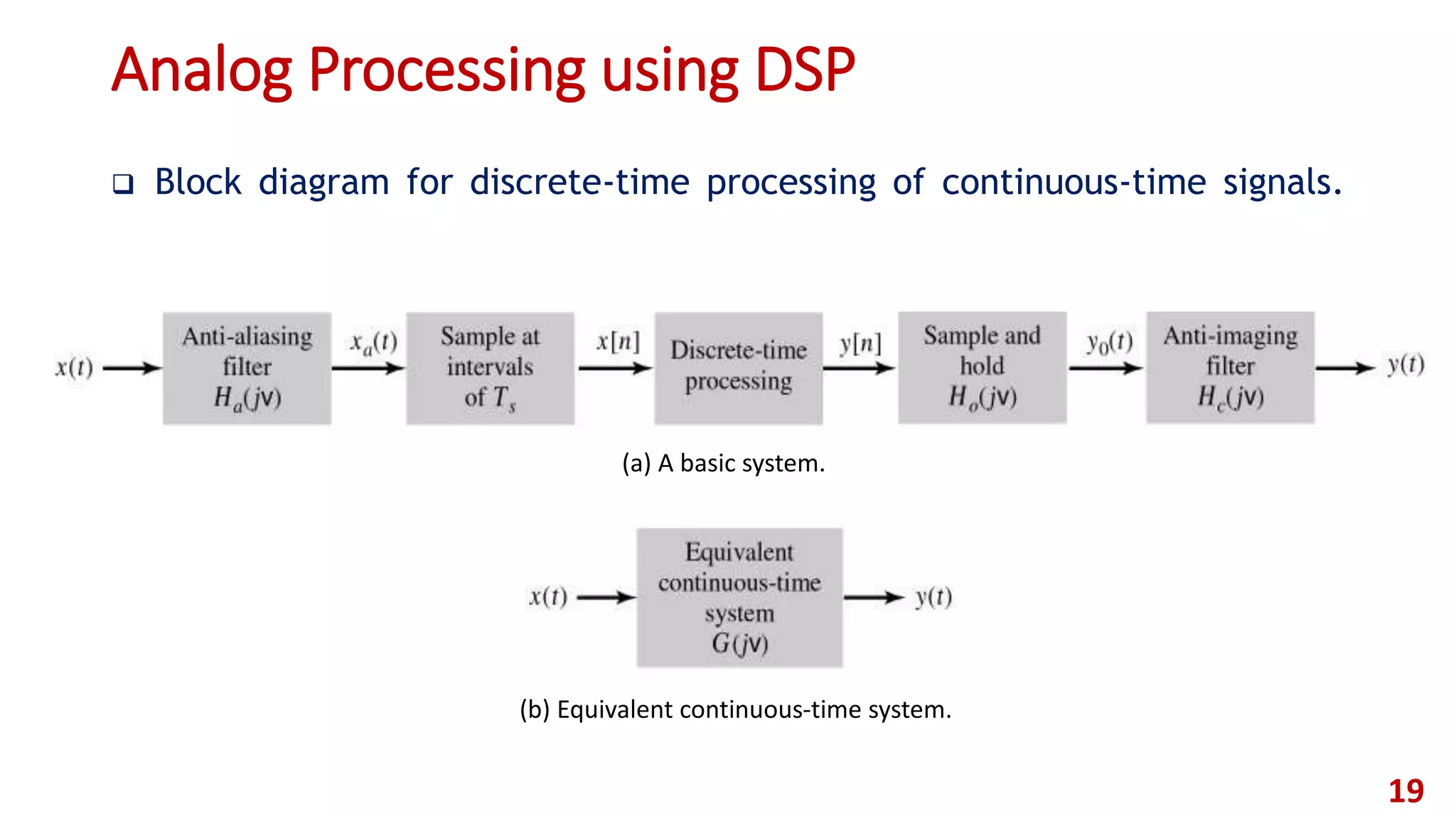
![Continuous to discrete (Ideal C/D) converter (Cont.)
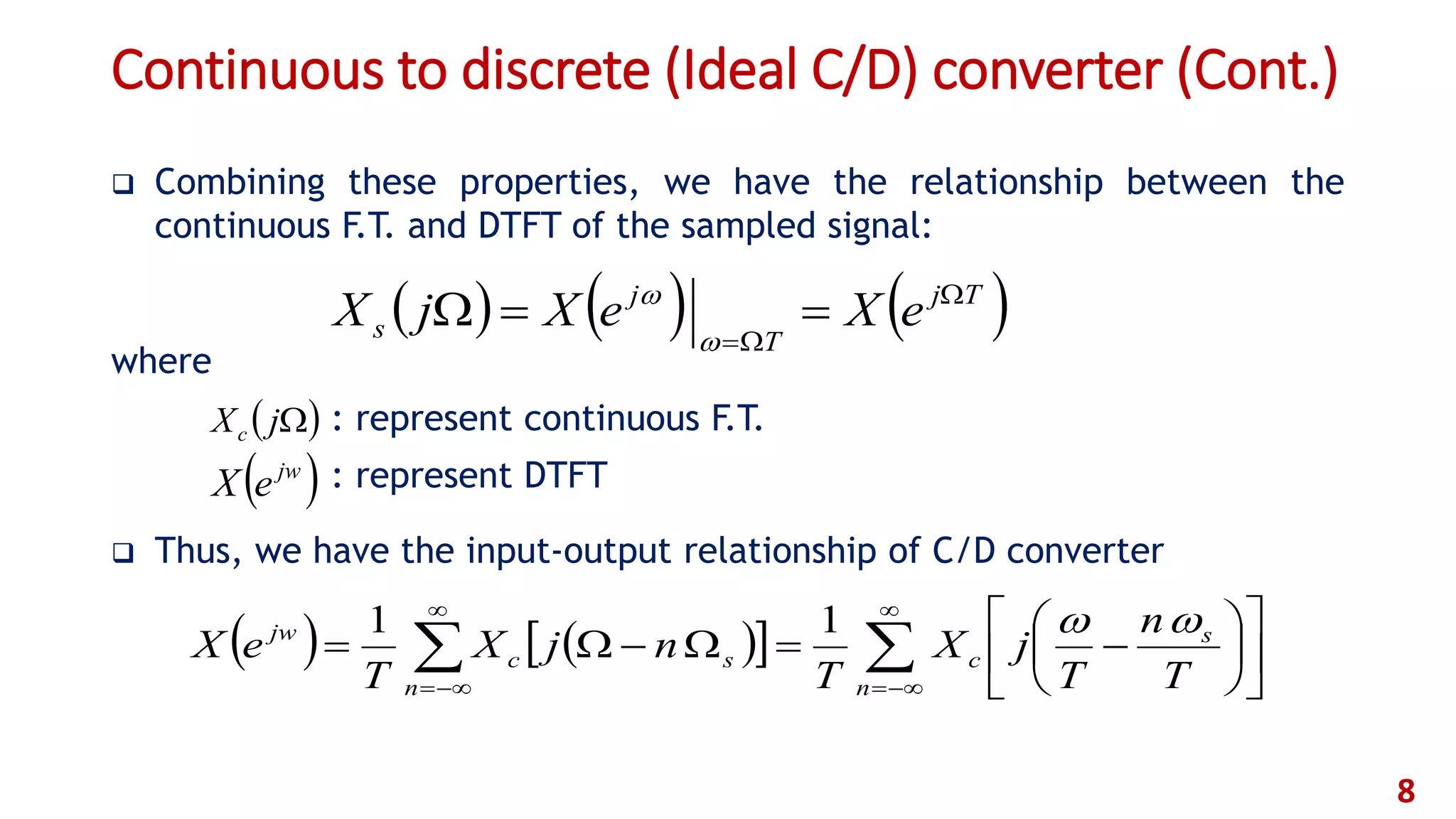
In the above, we characterize the relationship of 𝑥 𝑠(𝑡) and 𝑥 𝑐(𝑡) in the
continuous F.T. domain.
From another point of view, 𝑋𝑠(𝑗𝛺) can be represented as the linear
combination of a serious of complex exponentials:
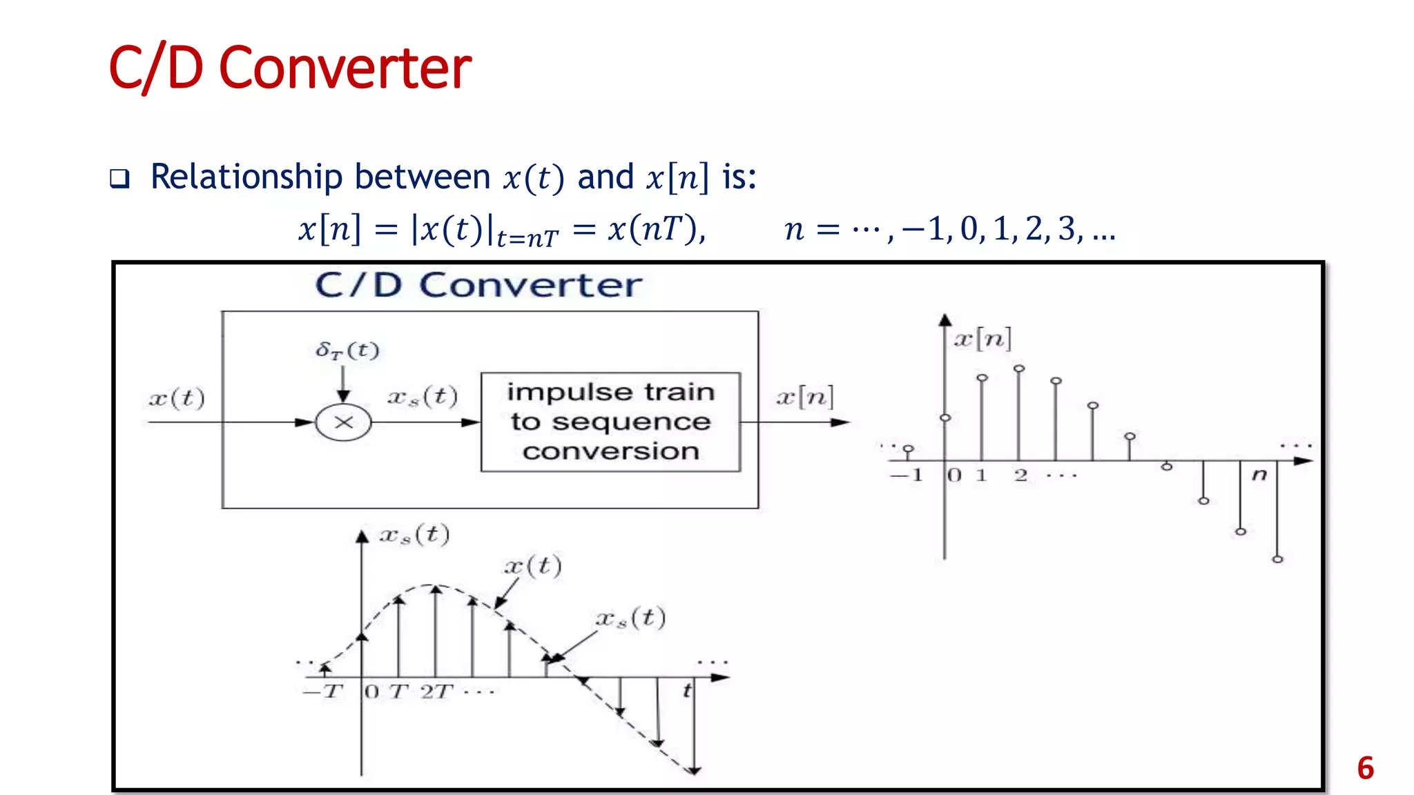
If 𝑥(𝑛𝑇) ≡ 𝑥[𝑛], its DTFT is
The relation between digital frequency and analog frequency is 𝝎 = 𝛀𝐓 7
n
cs nTtnTxtx since
n
Tnj
cs enTxjX
n
nj
n
njj
enTxenxeX
)(][)(](https://image.slidesharecdn.com/dsp2018foehu-lec10-multi-ratedigitalsignalprocessing-191223181400/75/Dsp-2018-foehu-lec-10-multi-rate-digital-signal-processing-7-2048.jpg)
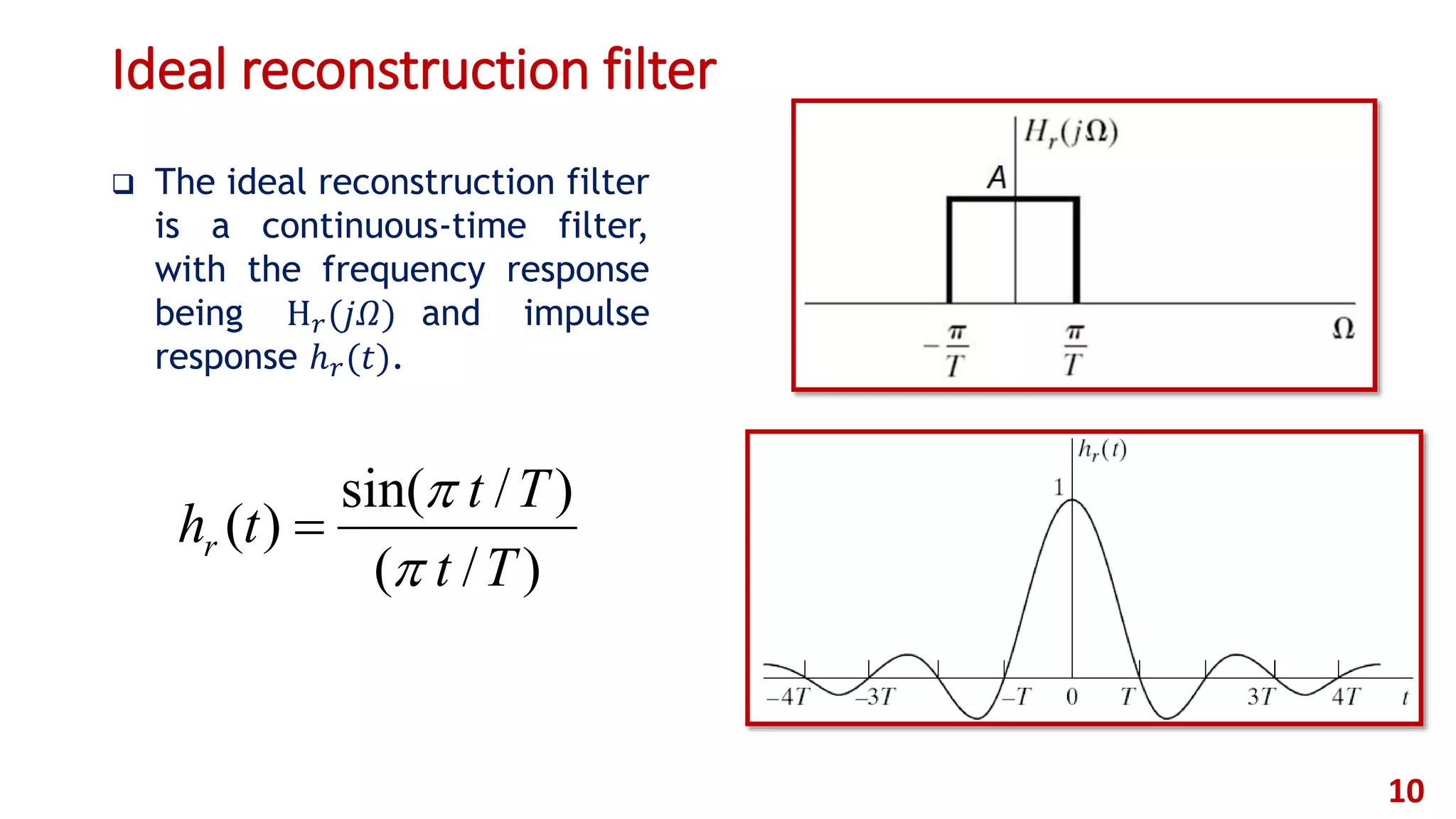
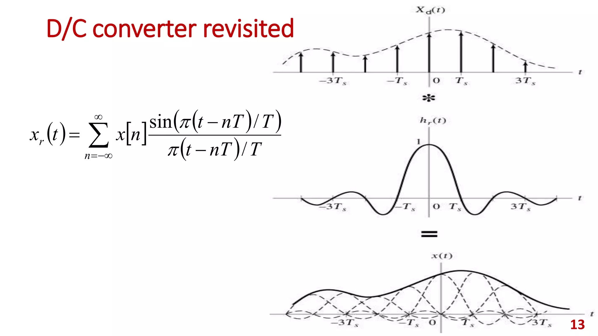
![D/C converter revisited
An ideal low-pass filter 𝐻(𝑒 𝑗𝜔) that has a cut-off frequency Ω 𝑐 = Ω 𝑠/2
= 𝜋/𝑇 and gain 𝐴 is used for reconstructing the continuous signal.
Frequency domain of D/C converter: [𝐻(𝑒 𝑗𝜔) is its frequency response]
Remember that the corresponding impulse response is a 𝑠𝑖𝑛𝑐 function, and
the reconstructed signal is
12
n
r
TnTt
TnTt
nyty
/
/sin
otherwise
TeYA
eYjHjY
Tj
Tj
rr
,0
/, ](https://image.slidesharecdn.com/dsp2018foehu-lec10-multi-ratedigitalsignalprocessing-191223181400/75/Dsp-2018-foehu-lec-10-multi-rate-digital-signal-processing-12-2048.jpg)
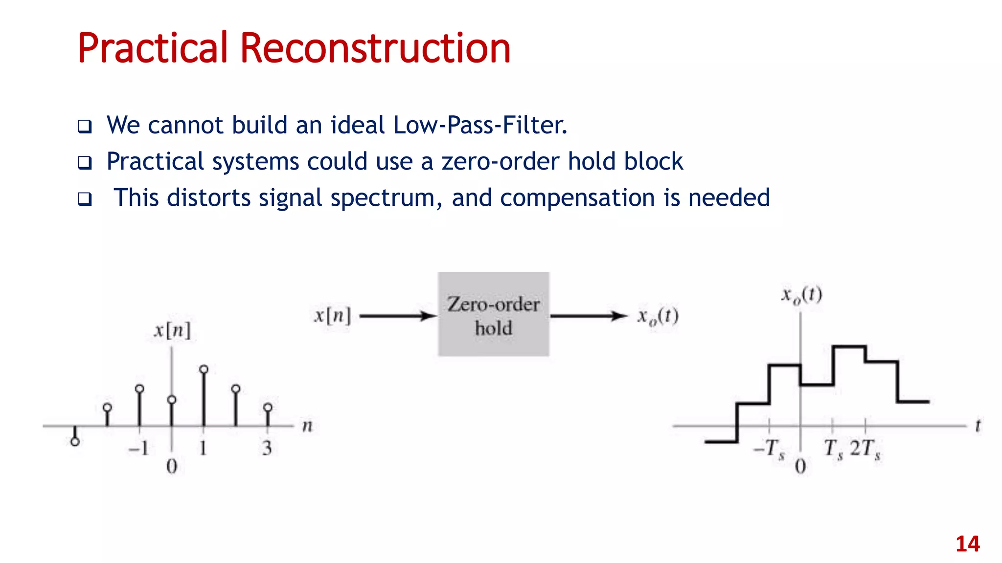
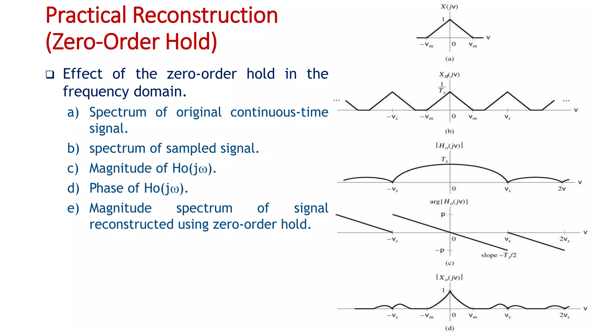
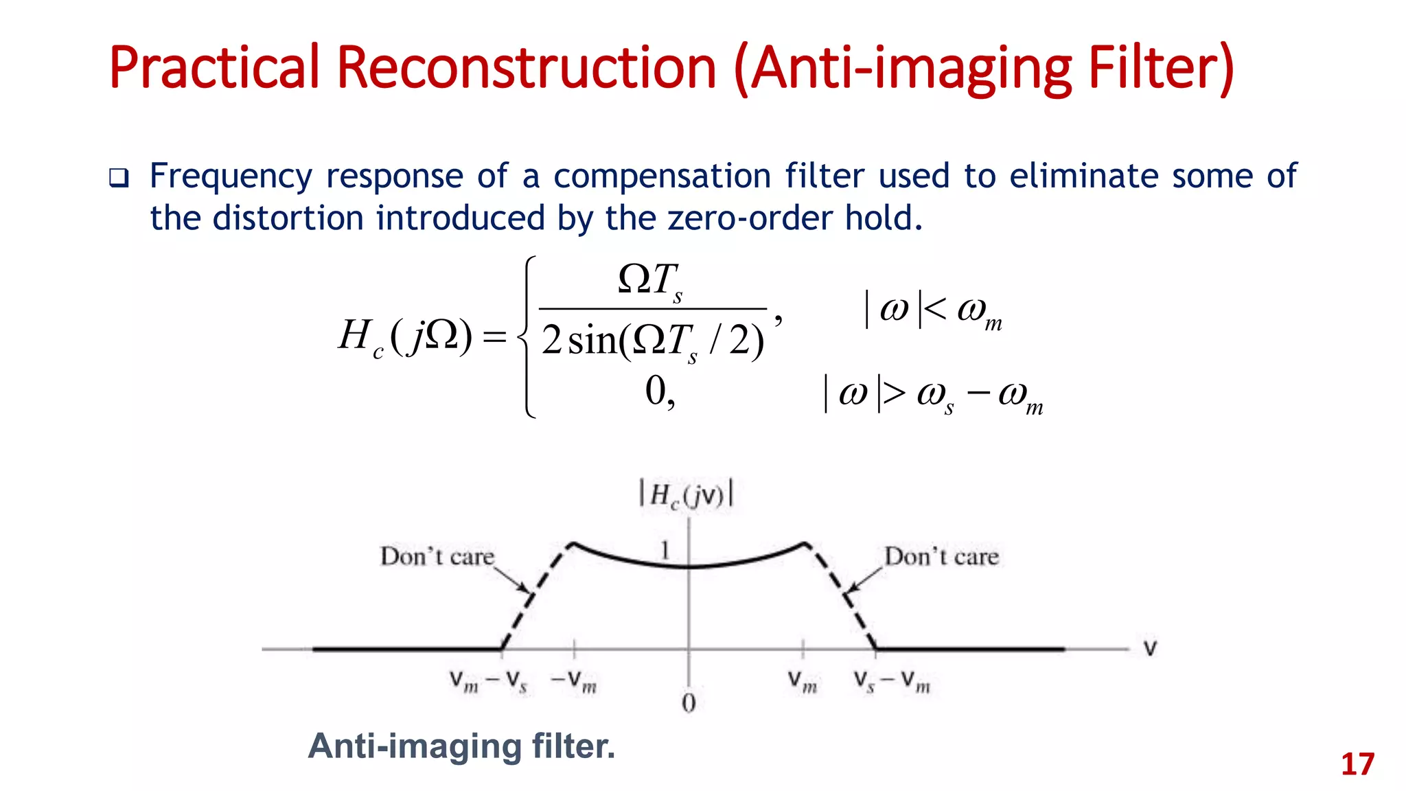
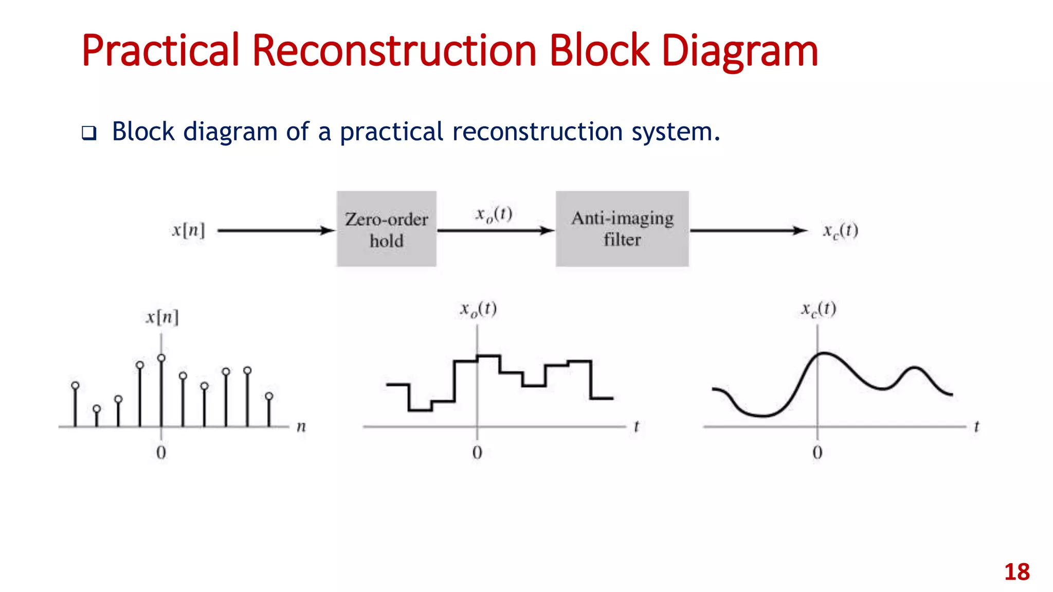
![Practical Reconstruction (Zero-Order Hold)
Rectangular pulse used to analyze zero-order hold reconstruction
15
s
s
Ttt
Tt
th
,0,0
0,1
)(0
n
s
n
s
nTthnx
nTtnxth
thtxtx
)(][
)(][)(
)()()(
0
0
00
)2/sin(
2)(
)()()(
2/
0
00
sTj T
ejH
jXjHjX
s
](https://image.slidesharecdn.com/dsp2018foehu-lec10-multi-ratedigitalsignalprocessing-191223181400/75/Dsp-2018-foehu-lec-10-multi-rate-digital-signal-processing-15-2048.jpg)
![Digital Signal Processing
Provided that :
𝐻 𝑎 𝑗Ω =
1 Ω ≤
Ω 𝑠
2
0 Ω >
Ω 𝑠
2
𝐺 𝑒𝑓𝑓 𝑗Ω =
𝐻 𝑎 𝑗Ω 𝐺 𝑒 𝑗Ω𝑇
𝐻 𝑜 𝑗Ω 𝐻𝑟 𝑗Ω Ω ≤
Ω 𝑠
2
0 Ω >
Ω 𝑠
2 23
Digital Signal
Processor
C/D
Sample
nT
𝑥(𝑡)
𝑋(𝑗Ω)
Antialiasing
Analog
Filter
𝑯 𝒂(𝒋𝛀)
𝑥 𝑎(𝑡)
𝑋 𝑎(𝑗Ω)
𝑥[𝑛]
𝑋(𝑒 𝑗𝜔
)
Reconstruction
Analog
Filter
𝑯 𝒓(𝒋𝛀)
𝑮(𝒆𝒋𝝎)
𝑦[𝑛]
𝑌(𝑒 𝑗𝜔
)
𝑦𝑎(𝑡)
𝑌𝑎(𝑗Ω)𝑯 𝒐(𝒋𝛀)
D/C
Zero order
hold
𝑦(𝑡)
𝑌(𝑗Ω)
𝑮 𝒆𝒇𝒇(𝒋𝛀)
𝑦(𝑡)
𝑌(𝑗Ω)𝑋(𝑗Ω)
𝑥(𝑡)](https://image.slidesharecdn.com/dsp2018foehu-lec10-multi-ratedigitalsignalprocessing-191223181400/75/Dsp-2018-foehu-lec-10-multi-rate-digital-signal-processing-23-2048.jpg)
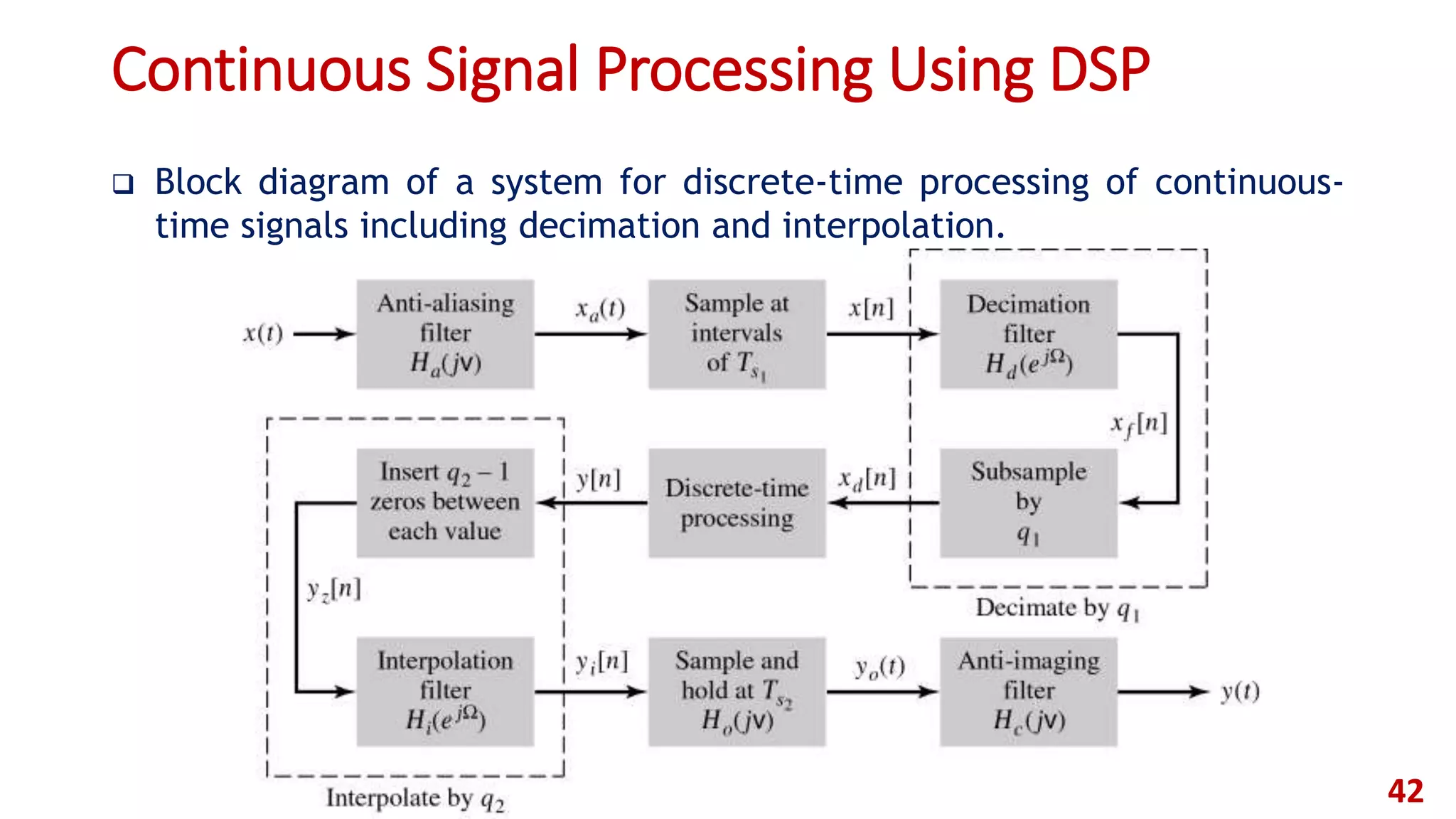
![Multirate Digital Signal Processing
The solution is changing sampling rate using downsampling and
upsampling.
Low cos:
Analog filter (eg. RC circuit)
Storage / Computation
Price:
Extra Computation for ↓ 𝑴 𝟏 and ↑ 𝑴 𝟐
Faster ADC and DAC
30
DSPC/D
Sample
nT
𝑥(𝑡)
𝑋(𝑗Ω)
Antialiasing
Analog
Filter
𝑯 𝒂(𝒋𝛀)
𝑥 𝑎(𝑡) 𝑥[𝑛]
Reconstruction
Analog
Filter
𝑯 𝒓(𝒋𝛀)
𝑮(𝒆𝒋𝝎
)
𝑦[𝑛] 𝑦𝑎(𝑡)
𝑯 𝒐(𝒋𝛀)
D/C
Zero order
hold 𝑦(𝑡)
𝑌(𝑗Ω)
↓ 𝑴 𝟏
Downsampler
𝑥1[𝑛]
↑ 𝑴 𝟐
Upsampler
𝑦2[𝑛]](https://image.slidesharecdn.com/dsp2018foehu-lec10-multi-ratedigitalsignalprocessing-191223181400/75/Dsp-2018-foehu-lec-10-multi-rate-digital-signal-processing-30-2048.jpg)
![Downsampling
Let 𝑥1 𝑛 and 𝑥2 𝑛 be obtained by sample 𝑥(𝑡) with sampling interval 𝑇 and MT,
respectively.
35
𝑥 𝑎(𝑡)
𝑋 𝑎(𝑗Ω) 𝑋1(𝑒 𝑗𝜔)
𝑥1[n]A/D
Sample @T
Ω 𝑠
𝑥 𝑎(𝑡)
𝑋 𝑎(𝑗Ω) 𝑋2(𝑒 𝑗𝜔
)
𝑥2[n]A/D
Sample @MT
Ω 𝑠/𝑀
T
MT
𝟐𝝅 𝟒𝝅𝟐𝝅𝟒𝝅 T𝛀 𝒐T𝛀 𝒐
𝟐𝝅 𝟒𝝅𝟐𝝅𝟒𝝅](https://image.slidesharecdn.com/dsp2018foehu-lec10-multi-ratedigitalsignalprocessing-191223181400/75/Dsp-2018-foehu-lec-10-multi-rate-digital-signal-processing-35-2048.jpg)
![Downsampling Block
𝑥[n]
𝑋(𝑒 𝑗𝜔
)
Discrete Time
Low-Pass Filter
𝐻 𝑑(𝑒 𝑗𝜔
)
𝑤[n]
𝑊(𝑒 𝑗𝜔
) 𝑌(𝑒 𝑗𝜔
)
𝑦 n = 𝑤[Mn]Discard Values
𝑛 ≠ 𝑀𝑙
𝝅
𝑴
𝝅
𝝅
𝑴
(d) Spectrum after Downsampling.
(c) Spectrum of filter output.
(b) Filter frequency response.
(a) Spectrum of oversampled input signal.
Noise is depicted as the shaded portions
of the spectrum.
𝑌(𝑒 𝑗𝜔)
𝑦 nDownsampler
↓ 𝑀
𝑥[n]
𝑋(𝑒 𝑗𝜔)](https://image.slidesharecdn.com/dsp2018foehu-lec10-multi-ratedigitalsignalprocessing-191223181400/75/Dsp-2018-foehu-lec-10-multi-rate-digital-signal-processing-36-2048.jpg)
![Downsampling Block
Note: if 𝑦 n = 𝑤[Mn], then
𝑌 𝑒 𝑗𝜔 =
1
𝑀
𝑚=0
𝑀−1
𝑋 𝑒 𝑗(𝜔−2𝜋𝑚)/𝑀
What does 𝑌 𝑒 𝑗𝜔
=
1
𝑀 𝑚=0
𝑀−1
𝑋 𝑒 𝑗(𝜔−2𝜋𝑚)/𝑀
represent?
Stretching of 𝑋(𝑒 𝑗𝜔) to 𝑋(𝑒 𝑗𝜔/𝑀)
Creating M − 1 copies of the stretched versions
Shifting each copy by successive multiples of 2𝜋 and superimposing (adding)
all the shifted copies
Dividing the result by M
37
Discrete Time
Low-Pass Filter
𝐻 𝑑(𝑒 𝑗𝜔
)
𝑤[n]
𝑊(𝑒 𝑗𝜔) 𝑌(𝑒 𝑗𝜔
)
𝑦 n = 𝑤[Mn]Discard Values
𝑛 ≠ 𝑀𝑙](https://image.slidesharecdn.com/dsp2018foehu-lec10-multi-ratedigitalsignalprocessing-191223181400/75/Dsp-2018-foehu-lec-10-multi-rate-digital-signal-processing-37-2048.jpg)
![Upsampling
Let 𝑥1 𝑛 and 𝑥2 𝑛 be obtained by sample 𝑥(𝑡) with sampling interval 𝑇 and T/M,
respectively.
38
𝑥 𝑎(𝑡)
𝑋 𝑎(𝑗Ω) 𝑋1(𝑒 𝑗𝜔)
𝑥1[n]A/D
Sample @T
Ω 𝑠
𝑥 𝑎(𝑡)
𝑋 𝑎(𝑗Ω) 𝑋2(𝑒 𝑗𝜔
)
𝑥2[n]A/D
Sample @T/M
𝑀 Ω 𝑠
M
T
T
𝟐𝝅 𝟒𝝅𝟐𝝅𝟒𝝅
𝟐𝝅 𝟒𝝅𝟐𝝅𝟒𝝅](https://image.slidesharecdn.com/dsp2018foehu-lec10-multi-ratedigitalsignalprocessing-191223181400/75/Dsp-2018-foehu-lec-10-multi-rate-digital-signal-processing-38-2048.jpg)
![Upsampling (zero padding) Block Diagram
39
Insert (M-1) zeros
between each two
successive samples
𝑥2[n]
𝑋2(𝑒 𝑗𝜔
)
Discrete Time
Low-Pass Filter
𝐻𝑖(𝑒 𝑗𝜔
)
𝑋𝑖(𝑒 𝑗𝜔
)
𝑥𝑖 nUpsampler
↑ 𝑀
𝑥[n]
𝑋(𝑒 𝑗𝜔
)](https://image.slidesharecdn.com/dsp2018foehu-lec10-multi-ratedigitalsignalprocessing-191223181400/75/Dsp-2018-foehu-lec-10-multi-rate-digital-signal-processing-39-2048.jpg)
![Upsampling (zero padding) Block Diagram
𝑥2 𝑛 =
𝑥[
𝑛
𝑀
]
𝑛
𝑀
𝑖𝑛𝑡𝑒𝑔𝑒𝑟
0 𝑜𝑡ℎ𝑒𝑟𝑤𝑖𝑠𝑒
or
𝑥2 𝑛 =
𝑘=−∞
∞
𝑥 𝑘 𝛿(𝑛 − 𝑘𝑀)
The frequency spectrum is
𝑋2(𝑒 𝑗𝜔
) =
𝑛=−∞
∞
𝑘=−∞
∞
𝑥 𝑘 𝛿(𝑛 − 𝑘𝑀) 𝑒−𝑗𝑛𝜔
𝑋2(𝑒 𝑗𝜔
) =
𝑘=−∞
∞
𝑥 𝑘
𝑛=−∞
∞
𝛿(𝑛 − 𝑘𝑀) 𝑒−𝑗𝑛𝜔
𝑋2 𝑒 𝑗𝜔 =
𝑘=−∞
∞
𝑥 𝑘 𝑒−𝑗𝑘𝑀𝜔 = 𝑋 𝑒 𝑗𝑀𝜔 = 𝑋 𝑒 𝑗 𝜔 , 𝑤ℎ𝑒𝑟𝑒 𝜔 = 𝑀𝜔
40](https://image.slidesharecdn.com/dsp2018foehu-lec10-multi-ratedigitalsignalprocessing-191223181400/75/Dsp-2018-foehu-lec-10-multi-rate-digital-signal-processing-40-2048.jpg)
![Upsampling (zero padding) Block Diagram
41
𝑥[n]
𝑋(𝑒 𝑗𝜔
)
Insert (M-1) zeros
between each two
successive samples
𝑥2[n]
𝑋2(𝑒 𝑗𝜔
) 𝑋𝑖(𝑒 𝑗𝜔
)
𝑥𝑖 nDiscrete Time
Low-Pass Filter
𝐻𝑖(𝑒 𝑗𝜔
) 𝑋𝑖(𝑒 𝑗𝜔)
𝑥𝑖 nUpsampler
↑ 𝑀
𝑥[n]
𝑋(𝑒 𝑗𝜔
)
(a) Spectrum of original sequence.
(b) Spectrum after inserting (M – 1) zeros in
between every value of the original sequence.
(c) Frequency response of a filter for removing
undesired replicates located at 2/M, 4/M, …,
(M – 1)2/M.
(d) Spectrum of interpolated sequence.
𝝅](https://image.slidesharecdn.com/dsp2018foehu-lec10-multi-ratedigitalsignalprocessing-191223181400/75/Dsp-2018-foehu-lec-10-multi-rate-digital-signal-processing-41-2048.jpg)


This document discusses multi-rate digital signal processing and concepts related to sampling continuous-time signals. It begins by introducing discrete-time processing of continuous signals using an ideal continuous-to-discrete converter. It then covers the Nyquist sampling theorem and relationships between continuous and discrete Fourier transforms. It discusses ideal and practical reconstruction using zero-order hold and anti-imaging filters. Finally, it introduces the concepts of downsampling and upsampling in multi-rate digital signal processing systems.


![Digital Signal Processing[ECEG-3171]-Ch1_L06](https://cdn.slidesharecdn.com/ss_thumbnails/dspl6ch2-180427094424-thumbnail.jpg?width=640&height=640&fit=bounds)


![Digital Signal Processing[ECEG-3171]-Ch1_L05](https://cdn.slidesharecdn.com/ss_thumbnails/dspl5ch2-180427094424-thumbnail.jpg?width=640&height=640&fit=bounds)