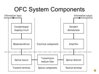
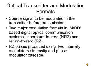
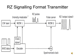
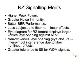
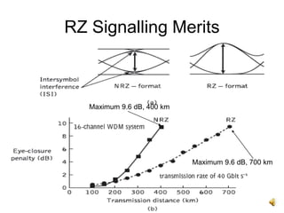
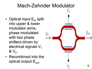
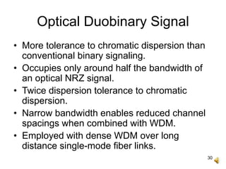
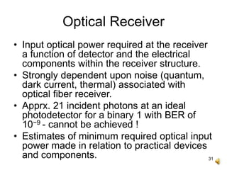
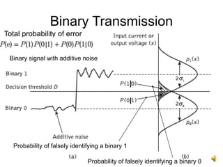
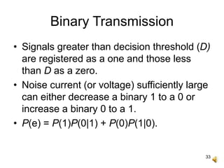
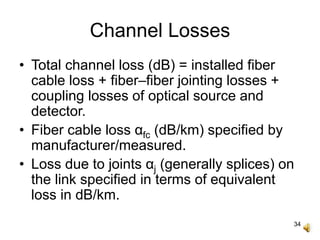
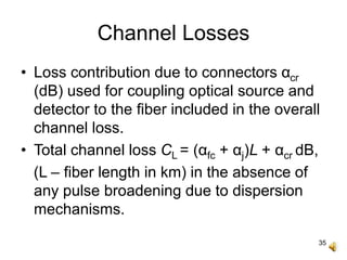
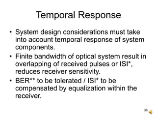
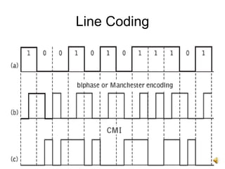
1
Digital Transmission Systems
MEC
2
Contents
• System Components.
• Digital Transmission.
• Quantization and Encoding.
• Pulse Code Modulation and IM/DD.
• Duobinary System.
• Binary Transmission.
• Channel Losses and Temporal Response.
• Line Coding.
3
OFC System Components
4
Digital Transmission Systems
• Superior performance over analog
counterparts.
• Ideal channel for data communications.
• Compatible with digital computing and
storage techniques.
• Optical fiber communication suited for
baseband digital transmission.
5
Digital Transmission Systems
• Acceptable SNR at optical fiber receiver
over analog transmission by 20 to 30 dB.
• Use of baseband digital signaling reduces
problems with optical source.
• Nonlinearities & temperature dependence
may severely affect analog transmission.
• Convey digital information in the baseband
using intensity modulation of the optical
source.
6
Digital Transmission Systems
• Pulse Code Modulation (PCM) – encoding
analog signal into digital bit pattern by initially
sampling the analog signal in excess of
Nyquist rate, Eg: for 3.4 kHz sampling rate is
8 kHz.
• Amplitude of constant width sampling pulses
varied in proportion to sample values of
analog signal, gives a discrete signal - pulse
amplitude modulation (PAM) - quantized to
discrete levels - PCM.
7
Quantization and Encoding
8
Digital Transmission Systems
• Digitized analog signal transmitted as a
baseband signal or be modulated by
amplitude, frequency or phase shift keying.
• Greater bandwidth required for PCM
transmission – optical channels are
wideband.
• Nonlinear encoding through companding -
input signal compressed before transmission,
expanded at the receive terminal after
decoding.
9
Companding
• Companding reduces quantization error on
small-amplitude analog signal levels when
encoded from PAM to PCM.
• Quantization error (rounding off to nearest
discrete level) exhibited as distortion or noise
on the signal (quantization noise).
• Companding tapers step size, reduces
distance between levels for small-amplitude
signals, increases distance between levels
for higher amplitude signals.
10
Companding
• Reduces quantization noise on small
amplitude signals at the expense of
slightly increased quantization noise for
larger signals.
• SNR improvement for small amplitude
signals reduces overall signal degradation.
• Converting continuous analog waveform
into discrete PCM signals permit time
division multiplexing.
11
Companding
12
Simplex Baseband PCM
Transmission
TDM
Simplex PCM
13
Digital Transmission Systems
• Received PCM waveform decoded back to
PAM, and then simply passed through a
low-pass filter, recovers original analog
signal.
• Encoded samples from different channels
interleaved within multiplexer to give a
single composite signal, transmitted over
the optical channel.
14
Digital Transmission Systems
• At receive terminal, interleaved samples
separated by synchronous switch or
demultiplexer.
• Analog signal reconstructed from the set of
samples.
• Time slots from channels interleaved
(multiplexed) into a frame, say of 32 time
slots.
• 2 additional time slots for signaling and
synchronization information, no encoded
speech.
15
Timing for Line Signalling
Bits per time slot
Time slots per frame
Frames per multiframe
16
Optical Transmitter and Modulation
Formats
• Average optical power launched into fiber
from the transmitter depends on type of
source used and required system bit rate.
• Laser launches around 1 mW, LED limited
to about 100 μW - both devices emit less
power at higher bit rates.
• LED gives reduced output at modulation
bandwidths in excess of 50 MHz, laser
output unaffected below 40 GHz.
17
Optical Transmitter and Modulation
Formats
• Source signal to be modulated in the
transmitter before transmission.
• Two major modulation formats in IM/DD*
based digital optical communication
systems - nonreturn-to-zero (NRZ) and
return-to-zero (RZ).
• RZ pulses produced using two intensity
modulators / intensity and phase
modulator cascade.
18
RZ Signalling Format Transmitter
*
19
RZ Signalling Merits
• Higher Peak Power.
• Greater Noise Immunity.
• Better BER Performance.
• Less subjected to fiber non-linear effects.
• Eye diagram for RZ format displays larger
vertical eye opening against NRZ.
• Narrow vertical eye opening (eye closure) -
intersymbol interference due to fiber
nonlinear effects.
• Greater tolerance to ISI for WDM signals.
20
RZ Signalling Merits
Maximum 9.6 dB, 400 km
Maximum 9.6 dB, 700 km
21
Return to Zero Signalling
• Chirped return-to-zero (CRZ) - prechirping
of the pulse with sign of chirp opposite to
that introduced by fiber dispersion.
• CRZ - Enhanced system performance due
to pulse compression effect through
prechirping, combats fiber link dispersion.
• Carrier-suppressed return-to-zero (CSRZ)
- alternate bit phase inversion process
removes or suppresses carrier component
from power spectral density of RZ signal –
longer transmission distances.
22
VSB-CSRZ
• Vestigal Side Band Carrier Suppressed –
partial removal of one sideband spectra
using optical filter.
• Increased spectral efficiency, decreased
channel spectrum requirements, reduced
channel spacing.
• Complete information of a VSB channel
contained in only half of its spectrum, other
half is redundant.
• Redundant information ignored/reproduced
from the other half.
23
Optical Fiber Multiplexed
Transmission/WDM
• Spectral efficiency - ratio of average
channel capacity to average channel
spacing - determines overall density of a
WDM system, Eg : WDM system 40
Gbit/s, channel spacing 100 GHz -
spectral efficiency for a conventional
binary signal will be 0.4 bit/s/Hz.
• Decrease channel spacing to increase
spectral efficiency.
24
Optical Fiber Multiplexed
Transmission/WDM
• If channel spacing decreased beyond
specific limit - overlapping of adjacent
channel information, degradation of data
signals.
• Use of efficient modulation formats -
alternate mark inversion (AMI) / duobinary
(DB) to decrease optical spectral band
occupied by a channel without decreasing
amount of information / data carried.
25
Duobinary Transmitter and
Receiver
XOR gate + adder + 1 bit delay
26
Duobinary Transmitter and
Receiver
• Transmitter - electrical duobinary
encoder, Mach–Zehnder modulator.
• Duobinary encoder consists of XOR gate,
adder and 1 bit delay circuit.
• Electrical duobinary data converted to
optical signal using both ON/OFF and 0/π
phase values.
• ON state optical signal with 0 phase
represents binary 1, ON state with π
phase indicates minus one level
corresponding to electrical duobinary
signal.
27
Duobinary Transmitter and
Receiver
• Zero level of electrical duobinary produced
by not transmitting an optical signal (i.e.
OFF).
• Binary data recovered by simply inverting
optical intensity modulated signal.
• Electrical signal recovered by direct
detection at photodiode then an electrical
signal inversion, no need to determine /
recover phase of the optical signal.
28
Mach-Zehnder Modulator
• Interferometric structure made from
material with strong electro-optic effect
(LiNbO3, GaAs, InP etc.).
• Applying electric fields to arms changes
optical path lengths, results in phase
modulation.
• Combining two arms with different phase
modulation converts phase modulation
into intensity modulation.
29
Mach-Zehnder Modulator
• Optical input Ein split
into upper & lower
modulator arms,
phase modulated
with two phase
shifters driven by
electrical signals V1
& V2.
• Recombined into the
optical output Eout.
30
Optical Duobinary Signal
• More tolerance to chromatic dispersion than
conventional binary signaling.
• Occupies only around half the bandwidth of
an optical NRZ signal.
• Twice dispersion tolerance to chromatic
dispersion.
• Narrow bandwidth enables reduced channel
spacings when combined with WDM.
• Employed with dense WDM over long
distance single-mode fiber links.
31
Optical Receiver
• Input optical power required at the receiver
a function of detector and the electrical
components within the receiver structure.
• Strongly dependent upon noise (quantum,
dark current, thermal) associated with
optical fiber receiver.
• Apprx. 21 incident photons at an ideal
photodetector for a binary 1 with BER of
10−9 - cannot be achieved !
• Estimates of minimum required optical input
power made in relation to practical devices
and components.
32
Binary Transmission
Binary signal with additive noise
Probability of falsely identifying a binary 1
Probability of falsely identifying a binary 0
Total probability of error
33
Binary Transmission
• Signals greater than decision threshold (D)
are registered as a one and those less
than D as a zero.
• Noise current (or voltage) sufficiently large
can either decrease a binary 1 to a 0 or
increase a binary 0 to a 1.
• P(e) = P(1)P(0|1) + P(0)P(1|0).
34
Channel Losses
• Total channel loss (dB) = installed fiber
cable loss + fiber–fiber jointing losses +
coupling losses of optical source and
detector.
• Fiber cable loss αfc (dB/km) specified by
manufacturer/measured.
• Loss due to joints αj (generally splices) on
the link specified in terms of equivalent
loss in dB/km.
35
Channel Losses
• Loss contribution due to connectors αcr
(dB) used for coupling optical source and
detector to the fiber included in the overall
channel loss.
• Total channel loss CL = (αfc + αj)L + αcr dB,
(L – fiber length in km) in the absence of
any pulse broadening due to dispersion
mechanisms.
36
Temporal Response
• System design considerations must take
into account temporal response of system
components.
• Finite bandwidth of optical system result in
overlapping of received pulses or ISI*,
reduces receiver sensitivity.
• BER** to be tolerated / ISI* to be
compensated by equalization within the
receiver.
37
Temporal Response
• Loss Penalty - increase in optical power at
the receiver - dispersion–equalization / ISI
penalty.
• Dispersion–equalization penalty:
• τe - 1/e full width pulse broadening due to
dispersion on the link, τ - bit interval / period.
DL significant in wide band systems.
38
Temporal Response
• For Gaussian-shaped pulses,
σ - rms pulse width.
• Bit rate BT is the reciprocal of bit interval τ,
• Total channel loss with dispersion –
equalization penalty:
39
Line Coding
• Efficient timing recovery & synchronization
(frame alignment), error detection and
correction at the receiver.
• Suitable shaping of transmitted signal
power spectral density.
• Binary codes insert extra symbols into the
information data stream.
• Two-level block codes (nBmB) convert
blocks of n bits to blocks of m bits, m > n.
40
Line Coding
• Biphase or Manchester encoding - 1B2B
code - 0 transmitted as 01, 1 as 10 – no
more than two consecutive identical
symbols.
• Coded mark inversion (CMI) code - 1B2B
code - 0 transmitted as 01, 1 alternately as
00 or 11.
• Error monitoring - parity check, disparity
between numbers of 1s and 0s, forward
error correction etc.
41
Line Coding
42
Thank You

Digital transmission systems

  • 1.
  • 2.
    2 Contents • System Components. •Digital Transmission. • Quantization and Encoding. • Pulse Code Modulation and IM/DD. • Duobinary System. • Binary Transmission. • Channel Losses and Temporal Response. • Line Coding.
  • 3.
  • 4.
    4 Digital Transmission Systems •Superior performance over analog counterparts. • Ideal channel for data communications. • Compatible with digital computing and storage techniques. • Optical fiber communication suited for baseband digital transmission.
  • 5.
    5 Digital Transmission Systems •Acceptable SNR at optical fiber receiver over analog transmission by 20 to 30 dB. • Use of baseband digital signaling reduces problems with optical source. • Nonlinearities & temperature dependence may severely affect analog transmission. • Convey digital information in the baseband using intensity modulation of the optical source.
  • 6.
    6 Digital Transmission Systems •Pulse Code Modulation (PCM) – encoding analog signal into digital bit pattern by initially sampling the analog signal in excess of Nyquist rate, Eg: for 3.4 kHz sampling rate is 8 kHz. • Amplitude of constant width sampling pulses varied in proportion to sample values of analog signal, gives a discrete signal - pulse amplitude modulation (PAM) - quantized to discrete levels - PCM.
  • 7.
  • 8.
    8 Digital Transmission Systems •Digitized analog signal transmitted as a baseband signal or be modulated by amplitude, frequency or phase shift keying. • Greater bandwidth required for PCM transmission – optical channels are wideband. • Nonlinear encoding through companding - input signal compressed before transmission, expanded at the receive terminal after decoding.
  • 9.
    9 Companding • Companding reducesquantization error on small-amplitude analog signal levels when encoded from PAM to PCM. • Quantization error (rounding off to nearest discrete level) exhibited as distortion or noise on the signal (quantization noise). • Companding tapers step size, reduces distance between levels for small-amplitude signals, increases distance between levels for higher amplitude signals.
  • 10.
    10 Companding • Reduces quantizationnoise on small amplitude signals at the expense of slightly increased quantization noise for larger signals. • SNR improvement for small amplitude signals reduces overall signal degradation. • Converting continuous analog waveform into discrete PCM signals permit time division multiplexing.
  • 11.
  • 12.
  • 13.
    13 Digital Transmission Systems •Received PCM waveform decoded back to PAM, and then simply passed through a low-pass filter, recovers original analog signal. • Encoded samples from different channels interleaved within multiplexer to give a single composite signal, transmitted over the optical channel.
  • 14.
    14 Digital Transmission Systems •At receive terminal, interleaved samples separated by synchronous switch or demultiplexer. • Analog signal reconstructed from the set of samples. • Time slots from channels interleaved (multiplexed) into a frame, say of 32 time slots. • 2 additional time slots for signaling and synchronization information, no encoded speech.
  • 15.
    15 Timing for LineSignalling Bits per time slot Time slots per frame Frames per multiframe
  • 16.
    16 Optical Transmitter andModulation Formats • Average optical power launched into fiber from the transmitter depends on type of source used and required system bit rate. • Laser launches around 1 mW, LED limited to about 100 μW - both devices emit less power at higher bit rates. • LED gives reduced output at modulation bandwidths in excess of 50 MHz, laser output unaffected below 40 GHz.
  • 17.
    17 Optical Transmitter andModulation Formats • Source signal to be modulated in the transmitter before transmission. • Two major modulation formats in IM/DD* based digital optical communication systems - nonreturn-to-zero (NRZ) and return-to-zero (RZ). • RZ pulses produced using two intensity modulators / intensity and phase modulator cascade.
  • 18.
  • 19.
    19 RZ Signalling Merits •Higher Peak Power. • Greater Noise Immunity. • Better BER Performance. • Less subjected to fiber non-linear effects. • Eye diagram for RZ format displays larger vertical eye opening against NRZ. • Narrow vertical eye opening (eye closure) - intersymbol interference due to fiber nonlinear effects. • Greater tolerance to ISI for WDM signals.
  • 20.
    20 RZ Signalling Merits Maximum9.6 dB, 400 km Maximum 9.6 dB, 700 km
  • 21.
    21 Return to ZeroSignalling • Chirped return-to-zero (CRZ) - prechirping of the pulse with sign of chirp opposite to that introduced by fiber dispersion. • CRZ - Enhanced system performance due to pulse compression effect through prechirping, combats fiber link dispersion. • Carrier-suppressed return-to-zero (CSRZ) - alternate bit phase inversion process removes or suppresses carrier component from power spectral density of RZ signal – longer transmission distances.
  • 22.
    22 VSB-CSRZ • Vestigal SideBand Carrier Suppressed – partial removal of one sideband spectra using optical filter. • Increased spectral efficiency, decreased channel spectrum requirements, reduced channel spacing. • Complete information of a VSB channel contained in only half of its spectrum, other half is redundant. • Redundant information ignored/reproduced from the other half.
  • 23.
    23 Optical Fiber Multiplexed Transmission/WDM •Spectral efficiency - ratio of average channel capacity to average channel spacing - determines overall density of a WDM system, Eg : WDM system 40 Gbit/s, channel spacing 100 GHz - spectral efficiency for a conventional binary signal will be 0.4 bit/s/Hz. • Decrease channel spacing to increase spectral efficiency.
  • 24.
    24 Optical Fiber Multiplexed Transmission/WDM •If channel spacing decreased beyond specific limit - overlapping of adjacent channel information, degradation of data signals. • Use of efficient modulation formats - alternate mark inversion (AMI) / duobinary (DB) to decrease optical spectral band occupied by a channel without decreasing amount of information / data carried.
  • 25.
  • 26.
    26 Duobinary Transmitter and Receiver •Transmitter - electrical duobinary encoder, Mach–Zehnder modulator. • Duobinary encoder consists of XOR gate, adder and 1 bit delay circuit. • Electrical duobinary data converted to optical signal using both ON/OFF and 0/π phase values. • ON state optical signal with 0 phase represents binary 1, ON state with π phase indicates minus one level corresponding to electrical duobinary signal.
  • 27.
    27 Duobinary Transmitter and Receiver •Zero level of electrical duobinary produced by not transmitting an optical signal (i.e. OFF). • Binary data recovered by simply inverting optical intensity modulated signal. • Electrical signal recovered by direct detection at photodiode then an electrical signal inversion, no need to determine / recover phase of the optical signal.
  • 28.
    28 Mach-Zehnder Modulator • Interferometricstructure made from material with strong electro-optic effect (LiNbO3, GaAs, InP etc.). • Applying electric fields to arms changes optical path lengths, results in phase modulation. • Combining two arms with different phase modulation converts phase modulation into intensity modulation.
  • 29.
    29 Mach-Zehnder Modulator • Opticalinput Ein split into upper & lower modulator arms, phase modulated with two phase shifters driven by electrical signals V1 & V2. • Recombined into the optical output Eout.
  • 30.
    30 Optical Duobinary Signal •More tolerance to chromatic dispersion than conventional binary signaling. • Occupies only around half the bandwidth of an optical NRZ signal. • Twice dispersion tolerance to chromatic dispersion. • Narrow bandwidth enables reduced channel spacings when combined with WDM. • Employed with dense WDM over long distance single-mode fiber links.
  • 31.
    31 Optical Receiver • Inputoptical power required at the receiver a function of detector and the electrical components within the receiver structure. • Strongly dependent upon noise (quantum, dark current, thermal) associated with optical fiber receiver. • Apprx. 21 incident photons at an ideal photodetector for a binary 1 with BER of 10−9 - cannot be achieved ! • Estimates of minimum required optical input power made in relation to practical devices and components.
  • 32.
    32 Binary Transmission Binary signalwith additive noise Probability of falsely identifying a binary 1 Probability of falsely identifying a binary 0 Total probability of error
  • 33.
    33 Binary Transmission • Signalsgreater than decision threshold (D) are registered as a one and those less than D as a zero. • Noise current (or voltage) sufficiently large can either decrease a binary 1 to a 0 or increase a binary 0 to a 1. • P(e) = P(1)P(0|1) + P(0)P(1|0).
  • 34.
    34 Channel Losses • Totalchannel loss (dB) = installed fiber cable loss + fiber–fiber jointing losses + coupling losses of optical source and detector. • Fiber cable loss αfc (dB/km) specified by manufacturer/measured. • Loss due to joints αj (generally splices) on the link specified in terms of equivalent loss in dB/km.
  • 35.
    35 Channel Losses • Losscontribution due to connectors αcr (dB) used for coupling optical source and detector to the fiber included in the overall channel loss. • Total channel loss CL = (αfc + αj)L + αcr dB, (L – fiber length in km) in the absence of any pulse broadening due to dispersion mechanisms.
  • 36.
    36 Temporal Response • Systemdesign considerations must take into account temporal response of system components. • Finite bandwidth of optical system result in overlapping of received pulses or ISI*, reduces receiver sensitivity. • BER** to be tolerated / ISI* to be compensated by equalization within the receiver.
  • 37.
    37 Temporal Response • LossPenalty - increase in optical power at the receiver - dispersion–equalization / ISI penalty. • Dispersion–equalization penalty: • τe - 1/e full width pulse broadening due to dispersion on the link, τ - bit interval / period. DL significant in wide band systems.
  • 38.
    38 Temporal Response • ForGaussian-shaped pulses, σ - rms pulse width. • Bit rate BT is the reciprocal of bit interval τ, • Total channel loss with dispersion – equalization penalty:
  • 39.
    39 Line Coding • Efficienttiming recovery & synchronization (frame alignment), error detection and correction at the receiver. • Suitable shaping of transmitted signal power spectral density. • Binary codes insert extra symbols into the information data stream. • Two-level block codes (nBmB) convert blocks of n bits to blocks of m bits, m > n.
  • 40.
    40 Line Coding • Biphaseor Manchester encoding - 1B2B code - 0 transmitted as 01, 1 as 10 – no more than two consecutive identical symbols. • Coded mark inversion (CMI) code - 1B2B code - 0 transmitted as 01, 1 alternately as 00 or 11. • Error monitoring - parity check, disparity between numbers of 1s and 0s, forward error correction etc.
  • 41.
  • 42.