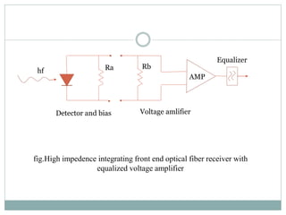
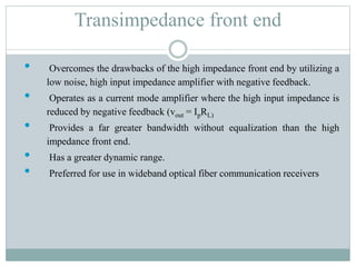
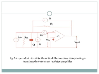
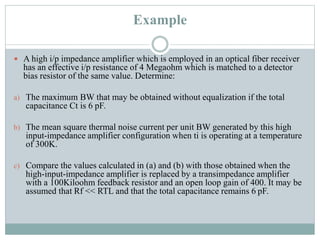
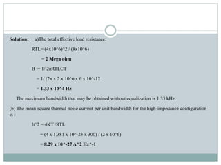
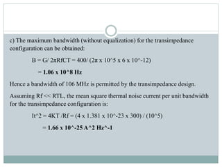
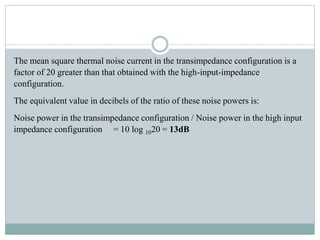
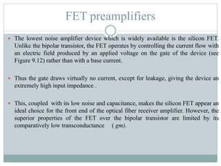
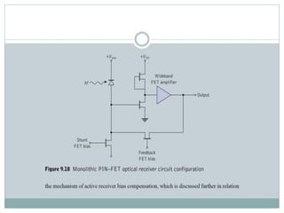
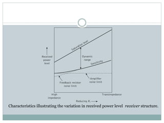
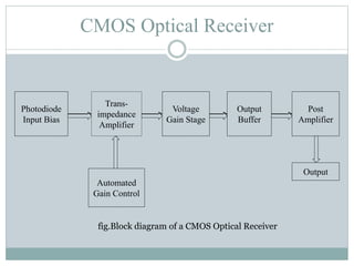
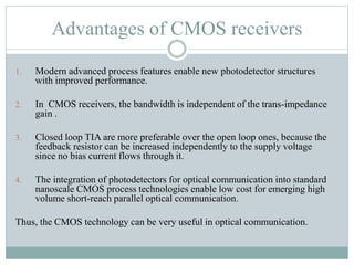
GOVERNMENT COLLEGE OF ENGINEERING
AURANGABAD
Presented By:
BE11F04F007 Sumedh Arak.
BE11F04F008 Priyanka Bagad.
BE11F04F009 Shraddha Bajaj
BE11F04F010 Shubham Bharajkar
Guided By:
Prof. A. S. Bhalchandra.
Optical Fiber Communication
Assignment on
“Receiver structures”
Receiver structures
• Optical detector is represented as a current source idet
• The noise sources (it, iTS and iamp)
• Amplifier
• Equalizer as a frequency shaping filter and may also apply selective phase
shifts to particular frequency components
fig.A full equivalent circuit for a digital optical fiber receiver
including various noises
Detector and bias Amplifier
Equalizer
AMP
idet
Vout
RL RaCd Ca
iamp
it iTS
Types of configurations
1. Low impedance front end
2. High impedance front end
3. Transimpedance front end
There are three types of digital optical fiber receiver
structures:
Low impedance front end
• Simplest and most common
• Low impedance front end allows thermal noise to dominate within the
receiver which limits its sensitivity
• Impractical for long-haul, wideband optical fiber communication
systems.
fig.Low impedance front end optical fiber receiver with voltage
amplifier
AMP
Ra Rb
hf
Detector and bias Voltage amplifier
High impedance front end
• High input impedance amplifier with large detector bias resistor to
reduce thermal noise.
• The detector output is effectively integrated over a large time constant
and must be restored by differentiation. This may be performed by the
correct equalization at a later stage and hence needs equalizer
• Improvement in sensitivity over the low impedance front end design,
but creates a heavy demand for equalization and has problems of
limited dynamic range causes by the attenuation of the low-frequency
signal components by the equalization process
fig.High impedence integrating front end optical fiber receiver with
equalized voltage amplifier
AMP
Ra Rb
hf
Detector and bias Voltage amlifier
Equalizer
Transimpedance front end
• Overcomes the drawbacks of the high impedance front end by utilizing a
low noise, high input impedance amplifier with negative feedback.
• Operates as a current mode amplifier where the high input impedance is
reduced by negative feedback (vout = IpRL)
• Provides a far greater bandwidth without equalization than the high
impedance front end.
• Has a greater dynamic range.
• Preferred for use in wideband optical fiber communication receivers
fig.An equivalent circuit for the optical fiber receiver incorporating a
transimpedance (current mode) preamplifier
-G
RTL
Vout
Vin
it
Rt
Va
iaCt
idet
Example
 A high i/p impedance amplifier which is employed in an optical fiber receiver
has an effective i/p resistance of 4 Megaohm which is matched to a detector
bias resistor of the same value. Determine:
a) The maximum BW that may be obtained without equalization if the total
capacitance Ct is 6 pF.
b) The mean square thermal noise current per unit BW generated by this high
input-impedance amplifier configuration when ti is operating at a temperature
of 300K.
c) Compare the values calculated in (a) and (b) with those obtained when the
high-input-impedance amplifier is replaced by a transimpedance amplifier
with a 100Kiloohm feedback resistor and an open loop gain of 400. It may be
assumed that Rf << RTL and that the total capacitance remains 6 pF.
Solution: a)The total effective load resistance:
RTL= (4x10^6)^2 / (8x10^6)
= 2 Mega ohm
B = 1/ 2πRTLCT
= 1/ (2π x 2 x 10^6 x 6 x 10^-12
= 1.33 x 10^4 Hz
The maximum bandwidth that may be obtained without equalization is 1.33 kHz.
(b) The mean square thermal noise current per unit bandwidth for the high-impedance configuration
is :
It^2 = 4KT /RTL
= (4 x 1.381 x 10^-23 x 300) / (2 x 10^6)
= 8.29 x 10^-27 A^2 Hz^-1
c) The maximum bandwidth (without equalization) for the transimpedance
configuration can be obtained:
B = G/ 2πRfCT = 400/ (2π x 10^5 x 6 x 10^-12)
= 1.06 x 10^8 Hz
Hence a bandwidth of 106 MHz is permitted by the transimpedance design.
Assuming Rf << RTL, the mean square thermal noise current per unit bandwidth
for the transimpedance configuration is:
It^2 = 4KT /Rf = (4 x 1.381 x 10^-23 x 300) / (10^5)
= 1.66 x 10^-25 A^2 Hz^-1
The mean square thermal noise current in the transimpedance configuration is a
factor of 20 greater than that obtained with the high-input-impedance
configuration.
The equivalent value in decibels of the ratio of these noise powers is:
Noise power in the transimpedance configuration / Noise power in the high input
impedance configuration = 10 log 1020 = 13dB
FET preamplifiers
 The lowest noise amplifier device which is widely available is the silicon FET.
Unlike the bipolar transistor, the FET operates by controlling the current flow with
an electric field produced by an applied voltage on the gate of the device (see
Figure 9.12) rather than with a base current.
 Thus the gate draws virtually no current, except for leakage, giving the device an
extremely high input impedance .
 This, coupled with its low noise and capacitance, makes the silicon FET appear an
ideal choice for the front end of the optical fiber receiver amplifier. However, the
superior properties of the FET over the bipolar transistor are limited by its
comparatively low transconductance ( gm).
Fig.Grounded source FET configuration for the front end of an optical fiber
receiver amplifier
 It can be shown that a figure of merit with regard to the noise performance of
the FET amplifier is gm/C2 T. Hence the advantage of high transconductance
together with low total capacitance CT is apparent.
 This requires FETs to be specifically matched to particular detectors. This is
especially the case for silicon FETs at frequencies above 25 MHz where the
current gain drops to values near unity as the transconductance is fixed with a
decreasing input impedance.
 Therefore at frequencies above 25 MHz, the bipolar transistor is a more useful
amplifying device.
 A large bias resistor has the effect of reducing the thermal noise but it will
also increase the low-frequency impedance of the detector load which tends
to integrate the signal (i.e. high-impedance integrating front-end).
 Thus compensation through equalization at a later stage is generally
required.
 Although silicon FETs have a limited useful bandwidth, much effort has
been devoted to the development of high-performance microwave FETs
since the mid-1970s.
 These FETs are fabricated from gallium arsenide and, being Schottky
barrier devices are called GaAs metal Schottky field effect transistors
(MESFETs).
Gallium Arsenide MESFETs
 They overcome the major disadvantage of silicon FETs in that they will
operate with both low noise and high gain at microwave frequencies (GHz).
 Thus in optical fiber communication receiver design they present an alternative
to bipolar transistors for wideband operation.
 The p–i–n/FET, or PIN–FET, hybrid receiver utilizes a high-performance
p–i–n photodiode followed by a low-noise preamplifier often based on a
GaAs MESFET, the whole of which is fabricated using thick-film
integrated circuit technology.
 This hybrid integration on a thick-film substrate reduces the stray
capacitance to negligible levels giving a total input capacitance which is
very low (e.g. 0.4 pF).
PIN–FET hybrid receivers
 The MESFETs employed have a transconductance of approximately 15
millisiemens at the bandwidths required.
 An example of a PIN–FET hybrid high impedance (integrating) front-
end receiver for operation at a wavelength of 1.3 μm using an In GaAs
p–i–n photodiode is shown in Figure 9.13 .
 As the high-impedance front end effectively integrates the signal, the
digital equalizer is necessary.
 The pulse shaping and noise filtering circuits comprise two passive filter
sections to ensure that the pulse waveform shape is optimized and the noise is
minimized.
 Equalization for the integration (i.e. differentiation) is performed by
monitoring the change in the integrated waveform over one period with a
subminiature coaxial delay line followed by a high-speed, low-level
comparator.
 The receiver is designed for use at a transmission rate of 140 Mbit s−1 where
its performance is found to be comparable to germanium and III–V alloy APD
receivers.
fig.PIN–FET hybrid high-impedance integrating front-end receiver
 The receiver is designed for use at a transmission rate of 140 Mbit s−1 where its
performance is found to be comparable to germanium and III–V alloy APD
receivers. For example, the receiver sensitivity at a BER of 10−9 is −44.2 dBm.
 Table 9.1 provides a comparison of typical sensitivities obtained with an
InGaAs hybrid PIN–FET receiver and an InAlAs APD receiver when both are
operating at a wavelength of 1.55 μm. The hybrid PIN–FET receiver design
displays a lower sensitivity than the APD receiver at a transmission rate of 2.5
Gbit s−1 and although it can also function at the higher transmission rate of 40
Gbit s−1, the PIN–FET receiver then exhibits a very poor sensitivity of only
−7.0 dBm.
Sensitivities for InGaAs PIN–FET and InAlAs APD receivers at the wavelength of 1.55 μm
Receiver type Sensitivity (dBm) Transmission rate
(Gbit s−1)
PIN–FET -23.0 2.5
APD -34.0 2.5
APD -29.0 10
APD -27.1 10
PIN–FET 7.0 40
High-performance receivers
 It is clear from the discussions in previous Sections that noise performance is
a major design consideration providing a limitation to the sensitivity.
 P–i–n photodiodes with GaAs MESFETs gives low-noise performance
combined with potential speed operation.
 At low speeds the three FET preamplifiers provide higher sensitivity than the
Si bipolar device.
 Below 10 Mbit s−1 the Si MOSFET preamplifier provides a lower noise
performance than the GaAs MESFET.
 Above 20 Mbit s−1, however, the highest sensitivity is obtained with the
GaAs MESFET device, even though at very high speeds the Si MOSFET
and Si bipolar transistor preamplifiers exhibit good noise performance
slightly worse than that of GaAs MESFET.
 Si bipolar transistor preamplifier displays a noise improvement over the Si
JFET, in this case at speeds above 50 Mbit s−1.
 A theoretical performance comparison for the silicon junction FET (JFET),
the silicon metal oxide semiconductor FET (MOSFET) and the silicon
bipolar transistor preamplifier with a GaAs MESFET device for
transmission rates from 1 Mbit s−1 to 10 Gbit s−1 shown in fig.
Noise characteristics for various optical receiver transistor preamplifiers
p–i–n–HEMT optical receiver
HEMT Optical Receiver
 New high-speed, low-noise transistor types have been invented for
optical receiver preamplifiers. These devices include the heterojunction
bipolar transistor (HBT) and high electron mobility transistor (HEMT).
 Each stage comprised a shunt feedback configuration containing a
single HEMT with mutual conductance of 70 millisiemens and a gate to
source capacitance of 0.36 pF. When operated with an In GaAs p–i–n
photodiode, the preamplifier exhibited a 21.5 dB gain over the range 100
MHz to 18 GHz.
fig.Circuit configuration for a high-sensitivity APD–FET optical receiver
APD–FET optical receiver
 Although the above discussion centered on p–i–n receiver preamplifier
designs, high speed APD optical receivers have also been invented.
Following fig. shows diagram of Circuit configuration for a high-sensitivity
APD–FET optical receiver.
 In particular, a high-sensitivity APD–FET receiver designed to operate at
speeds up to 8 Gbit s−1 and at wavelengths in the range 1.3 to 1.5 μm is
shown in above Figure . The receiver employed a 60 GHz gain–bandwidth
product InGaAs/InPAPD followed by a hybrid GaAs MESFET high-
impedance front end.
 Another strategy for the provision of wideband, low-noise receivers, especially
using the p–i–n photodiode detector, involves the monolithic integration of this
device type with semiconductor alloy FETs or HBTs.
 The design comprises a voltage variable FET feedback resistor which
produces active feedback as an input shunt automatic gain control (AGC)
circuit which extends the dynamic range by diverting excess photocurrent
away from the input of the basic receiver.
 Furthermore, the shunt FET gives additional dynamic range extension
through the mechanism of active receiver bias compensation.
Dynamic range and sensitivity
characteristics
 The receiver dynamic range is an important performance parameter as it
provides a measure of the difference between the device sensitivity and its
saturation or overload level.
 The difference between the two latter receiver structures may be observed in
the dynamic range and sensitivity characteristics shown in following Figure
Characteristics illustrating the variation in received power level receiver structure.
 Although the sensitivity decreases in moving from the high-impedance design
(left hand side) to the transimpedance configuration (right hand side) as the
value of the feedback resistor Rf is reduced.
 The saturation level increases at a faster rate, producing a significantly wider
dynamic range for the transimpedance front-end receiver.
Active receiver bias compensation
fig. active receiver bias compensation
 As the d.c. voltage at the input to the amplifier increases with the
incident optical power, the control loop applies an equal but opposite
shift in the voltage to the other side of the bias resistor.
 In this way the voltage at the input to the preamplifier becomes
independent of the detected power level.
 However, in practice the feedback voltage in the control loop cannot be
unbounded and therefore the technique has limitations.
 Even when using bias compensation with a high-impedance front-end receiver
to improve the saturation level, the overall dynamic range tends to be poor. For
such a receiver operating at a speed of 1 Gbit s−1 it is usually in the range 20
to 27 dB.
 The dynamic range can be 30 to 39 dB.* Furthermore, in the latter case
alternative design strategies have proved successful in increasing the receiver
dynamic range.
Optical Feedback Technique
fig.circuit diagram for Optical Feedback technique
 The optical feedback technique, which is shown schematically in above
Figure, eliminates the thermal noise associated with the feedback resistor in
the transimpedance frontend design.
 This strategy proves most useful at low transmission rates because in this case
the feedback resistors employed are normally far smaller than the optimum
value for low-noise performance so as to maintain the resistor at a practical
size (e.g. 1 MΩ).
 Employ pre-amplification using an optical amplifier prior to the Receiver.
 Two basic optical amplifier technological types, namely the semiconductor
optical amplifier (SOA) and the fiber amplifier or the EDFA.
 The SOA operates as a near-traveling-wave amplifier and therefore the
output emissions are spontaneous, creating a spectral bandwidth which is
determined by the gain profile of the device.
(Cont’d)
•
Alternative method
High performance receivers
 Because the typical spectral bandwidth is in the range 80 to 120 nm, a
bandpass optical filter is employed to reduce the intensity of the spontaneous
emission reaching the optical detector.
 Thus the effect of reducing the spontaneous noise products and thus improving
the overall receiver sensitivity.
 The SOA preamplifier p–i–n photodiode Configuration displays a significant
improvement over high performance APD receivers.
 The majority of the optical receivers operate at transmission rates from 10 to
40 Gbit /s and that both the SOA and erbium-doped fiber amplifier (EDFA) are
useful devices to provide for the optical pre-amplification.
(Cont’d)
High performance receivers
 Furthermore, the EDFA device can attain a receiver sensitivity of −25 dBm
with a noise figure value lying between 4 and 5 dB while enabling a high
transmission rate of 40 Gbit /s .
 The SOA, however, exhibits a relatively high noise figure in the range 7 to 8
dB, but its small size, wider operating wavelength range and potential for
monolithic integration make it an important device for optical pre-
amplification.
(Cont’d)
What is an EDFA?
 Finally , the Ge-on-silicon-on-
insulator(Ge-on-SOI) photodiodes
receiver are recently used.
 Error-free (BER<10-12) operation of
receivers combining a Ge-on-SOI
photodiode with a single-ended high-
speed receiver front using a supply
voltage of 1.8 V.
 In addition, receivers utilizing Ge-on-
SOI photodiodes integrated with a
low-power CMOS IC operate at 10
Gb/s using a single 1.1-V supply while
consuming only 11 mW of power.
High performance receivers
A CMOS receiver using 0.18 μm technology
Photodetector
(GaAs ,etc)
TIA(SiGe ,Bi
CMOS)
CDR ,digital
Photodetector
(GaAs ,etc)
TIA
(SiGe ,Bi
CMOS) CDR,digital
(a) Ordinary receiver
(b)CMOS receiver
CMOS Optical Receiver
Photodiode
Input Bias
Trans-
impedance
Amplifier
Voltage
Gain Stage
Output
Buffer
Post
Amplifier
Automated
Gain Control
Output
fig.Block diagram of a CMOS Optical Receiver
 There has been significant recent progress towards the realization of multi-
gbps optical receivers fully integrated into standard CMOS processes.
 Trans-impedance amplifier (TIA) gives wide bandwidth, high gain, low
input referred noise and wide dynamic range.
 The Automated Gain Control (AGC) voltage is used to provide variable
gain for multilevel signals.
 This design is simulated in 0.18 μm UMC (United Microelectronics
Corporation)technology for the performance analysis.
 The bandwidth range is 7.03 GHz to 11.5 GHz corresponding to 0 - 3 V
AGC respectively.
 The input referred noise level value is 43.86 pA/Hz up to 10 GHz
frequency.
(Cont’d)
CMOS receivers
 The topology used is the transimpedance (TIA) amplifier, whose relative
low input impedance and wide bandwidth is well suited for the application.
 In the design of fixed-gain trans-impedance feedback amplifiers, there is a
direct relation between input noise current and the input current overload
level.
 Therefore, in order to enlarge the dynamic range, various means have been
adopted to vary the gain of the trans-impedance amplifiers in response to the
input signal levels.
 Variable-gain trans-impedance feedback amplifiers , however, are prone to
instability.
(Cont’d)
CMOS receivers
Fig.CMOS photodetector array in a standard 65-nm CMOS process.
CMOS receivers
Advantages of CMOS receivers
1. Modern advanced process features enable new photodetector structures
with improved performance.
2. In CMOS receivers, the bandwidth is independent of the trans-impedance
gain .
3. Closed loop TIA are more preferable over the open loop ones, because the
feedback resistor can be increased independently to the supply voltage
since no bias current flows through it.
4. The integration of photodetectors for optical communication into standard
nanoscale CMOS process technologies enable low cost for emerging high
volume short-reach parallel optical communication.
Thus, the CMOS technology can be very useful in optical communication.
Thank you!!!

Receiver structures(optical communication)

  • 1.
    GOVERNMENT COLLEGE OFENGINEERING AURANGABAD Presented By: BE11F04F007 Sumedh Arak. BE11F04F008 Priyanka Bagad. BE11F04F009 Shraddha Bajaj BE11F04F010 Shubham Bharajkar Guided By: Prof. A. S. Bhalchandra. Optical Fiber Communication Assignment on “Receiver structures”
  • 2.
    Receiver structures • Opticaldetector is represented as a current source idet • The noise sources (it, iTS and iamp) • Amplifier • Equalizer as a frequency shaping filter and may also apply selective phase shifts to particular frequency components
  • 3.
    fig.A full equivalentcircuit for a digital optical fiber receiver including various noises Detector and bias Amplifier Equalizer AMP idet Vout RL RaCd Ca iamp it iTS
  • 4.
    Types of configurations 1.Low impedance front end 2. High impedance front end 3. Transimpedance front end There are three types of digital optical fiber receiver structures:
  • 5.
    Low impedance frontend • Simplest and most common • Low impedance front end allows thermal noise to dominate within the receiver which limits its sensitivity • Impractical for long-haul, wideband optical fiber communication systems.
  • 6.
    fig.Low impedance frontend optical fiber receiver with voltage amplifier AMP Ra Rb hf Detector and bias Voltage amplifier
  • 7.
    High impedance frontend • High input impedance amplifier with large detector bias resistor to reduce thermal noise. • The detector output is effectively integrated over a large time constant and must be restored by differentiation. This may be performed by the correct equalization at a later stage and hence needs equalizer • Improvement in sensitivity over the low impedance front end design, but creates a heavy demand for equalization and has problems of limited dynamic range causes by the attenuation of the low-frequency signal components by the equalization process
  • 8.
    fig.High impedence integratingfront end optical fiber receiver with equalized voltage amplifier AMP Ra Rb hf Detector and bias Voltage amlifier Equalizer
  • 9.
    Transimpedance front end •Overcomes the drawbacks of the high impedance front end by utilizing a low noise, high input impedance amplifier with negative feedback. • Operates as a current mode amplifier where the high input impedance is reduced by negative feedback (vout = IpRL) • Provides a far greater bandwidth without equalization than the high impedance front end. • Has a greater dynamic range. • Preferred for use in wideband optical fiber communication receivers
  • 10.
    fig.An equivalent circuitfor the optical fiber receiver incorporating a transimpedance (current mode) preamplifier -G RTL Vout Vin it Rt Va iaCt idet
  • 11.
    Example  A highi/p impedance amplifier which is employed in an optical fiber receiver has an effective i/p resistance of 4 Megaohm which is matched to a detector bias resistor of the same value. Determine: a) The maximum BW that may be obtained without equalization if the total capacitance Ct is 6 pF. b) The mean square thermal noise current per unit BW generated by this high input-impedance amplifier configuration when ti is operating at a temperature of 300K. c) Compare the values calculated in (a) and (b) with those obtained when the high-input-impedance amplifier is replaced by a transimpedance amplifier with a 100Kiloohm feedback resistor and an open loop gain of 400. It may be assumed that Rf << RTL and that the total capacitance remains 6 pF.
  • 12.
    Solution: a)The totaleffective load resistance: RTL= (4x10^6)^2 / (8x10^6) = 2 Mega ohm B = 1/ 2πRTLCT = 1/ (2π x 2 x 10^6 x 6 x 10^-12 = 1.33 x 10^4 Hz The maximum bandwidth that may be obtained without equalization is 1.33 kHz. (b) The mean square thermal noise current per unit bandwidth for the high-impedance configuration is : It^2 = 4KT /RTL = (4 x 1.381 x 10^-23 x 300) / (2 x 10^6) = 8.29 x 10^-27 A^2 Hz^-1
  • 13.
    c) The maximumbandwidth (without equalization) for the transimpedance configuration can be obtained: B = G/ 2πRfCT = 400/ (2π x 10^5 x 6 x 10^-12) = 1.06 x 10^8 Hz Hence a bandwidth of 106 MHz is permitted by the transimpedance design. Assuming Rf << RTL, the mean square thermal noise current per unit bandwidth for the transimpedance configuration is: It^2 = 4KT /Rf = (4 x 1.381 x 10^-23 x 300) / (10^5) = 1.66 x 10^-25 A^2 Hz^-1
  • 14.
    The mean squarethermal noise current in the transimpedance configuration is a factor of 20 greater than that obtained with the high-input-impedance configuration. The equivalent value in decibels of the ratio of these noise powers is: Noise power in the transimpedance configuration / Noise power in the high input impedance configuration = 10 log 1020 = 13dB
  • 15.
    FET preamplifiers  Thelowest noise amplifier device which is widely available is the silicon FET. Unlike the bipolar transistor, the FET operates by controlling the current flow with an electric field produced by an applied voltage on the gate of the device (see Figure 9.12) rather than with a base current.  Thus the gate draws virtually no current, except for leakage, giving the device an extremely high input impedance .  This, coupled with its low noise and capacitance, makes the silicon FET appear an ideal choice for the front end of the optical fiber receiver amplifier. However, the superior properties of the FET over the bipolar transistor are limited by its comparatively low transconductance ( gm).
  • 16.
    Fig.Grounded source FETconfiguration for the front end of an optical fiber receiver amplifier
  • 17.
     It canbe shown that a figure of merit with regard to the noise performance of the FET amplifier is gm/C2 T. Hence the advantage of high transconductance together with low total capacitance CT is apparent.  This requires FETs to be specifically matched to particular detectors. This is especially the case for silicon FETs at frequencies above 25 MHz where the current gain drops to values near unity as the transconductance is fixed with a decreasing input impedance.  Therefore at frequencies above 25 MHz, the bipolar transistor is a more useful amplifying device.
  • 18.
     A largebias resistor has the effect of reducing the thermal noise but it will also increase the low-frequency impedance of the detector load which tends to integrate the signal (i.e. high-impedance integrating front-end).  Thus compensation through equalization at a later stage is generally required.
  • 19.
     Although siliconFETs have a limited useful bandwidth, much effort has been devoted to the development of high-performance microwave FETs since the mid-1970s.  These FETs are fabricated from gallium arsenide and, being Schottky barrier devices are called GaAs metal Schottky field effect transistors (MESFETs). Gallium Arsenide MESFETs
  • 20.
     They overcomethe major disadvantage of silicon FETs in that they will operate with both low noise and high gain at microwave frequencies (GHz).  Thus in optical fiber communication receiver design they present an alternative to bipolar transistors for wideband operation.
  • 21.
     The p–i–n/FET,or PIN–FET, hybrid receiver utilizes a high-performance p–i–n photodiode followed by a low-noise preamplifier often based on a GaAs MESFET, the whole of which is fabricated using thick-film integrated circuit technology.  This hybrid integration on a thick-film substrate reduces the stray capacitance to negligible levels giving a total input capacitance which is very low (e.g. 0.4 pF). PIN–FET hybrid receivers
  • 22.
     The MESFETsemployed have a transconductance of approximately 15 millisiemens at the bandwidths required.  An example of a PIN–FET hybrid high impedance (integrating) front- end receiver for operation at a wavelength of 1.3 μm using an In GaAs p–i–n photodiode is shown in Figure 9.13 .  As the high-impedance front end effectively integrates the signal, the digital equalizer is necessary.
  • 23.
     The pulseshaping and noise filtering circuits comprise two passive filter sections to ensure that the pulse waveform shape is optimized and the noise is minimized.  Equalization for the integration (i.e. differentiation) is performed by monitoring the change in the integrated waveform over one period with a subminiature coaxial delay line followed by a high-speed, low-level comparator.  The receiver is designed for use at a transmission rate of 140 Mbit s−1 where its performance is found to be comparable to germanium and III–V alloy APD receivers.
  • 24.
    fig.PIN–FET hybrid high-impedanceintegrating front-end receiver
  • 25.
     The receiveris designed for use at a transmission rate of 140 Mbit s−1 where its performance is found to be comparable to germanium and III–V alloy APD receivers. For example, the receiver sensitivity at a BER of 10−9 is −44.2 dBm.  Table 9.1 provides a comparison of typical sensitivities obtained with an InGaAs hybrid PIN–FET receiver and an InAlAs APD receiver when both are operating at a wavelength of 1.55 μm. The hybrid PIN–FET receiver design displays a lower sensitivity than the APD receiver at a transmission rate of 2.5 Gbit s−1 and although it can also function at the higher transmission rate of 40 Gbit s−1, the PIN–FET receiver then exhibits a very poor sensitivity of only −7.0 dBm.
  • 26.
    Sensitivities for InGaAsPIN–FET and InAlAs APD receivers at the wavelength of 1.55 μm Receiver type Sensitivity (dBm) Transmission rate (Gbit s−1) PIN–FET -23.0 2.5 APD -34.0 2.5 APD -29.0 10 APD -27.1 10 PIN–FET 7.0 40
  • 27.
    High-performance receivers  Itis clear from the discussions in previous Sections that noise performance is a major design consideration providing a limitation to the sensitivity.  P–i–n photodiodes with GaAs MESFETs gives low-noise performance combined with potential speed operation.  At low speeds the three FET preamplifiers provide higher sensitivity than the Si bipolar device.  Below 10 Mbit s−1 the Si MOSFET preamplifier provides a lower noise performance than the GaAs MESFET.
  • 28.
     Above 20Mbit s−1, however, the highest sensitivity is obtained with the GaAs MESFET device, even though at very high speeds the Si MOSFET and Si bipolar transistor preamplifiers exhibit good noise performance slightly worse than that of GaAs MESFET.  Si bipolar transistor preamplifier displays a noise improvement over the Si JFET, in this case at speeds above 50 Mbit s−1.
  • 29.
     A theoreticalperformance comparison for the silicon junction FET (JFET), the silicon metal oxide semiconductor FET (MOSFET) and the silicon bipolar transistor preamplifier with a GaAs MESFET device for transmission rates from 1 Mbit s−1 to 10 Gbit s−1 shown in fig.
  • 30.
    Noise characteristics forvarious optical receiver transistor preamplifiers
  • 31.
  • 32.
     New high-speed,low-noise transistor types have been invented for optical receiver preamplifiers. These devices include the heterojunction bipolar transistor (HBT) and high electron mobility transistor (HEMT).  Each stage comprised a shunt feedback configuration containing a single HEMT with mutual conductance of 70 millisiemens and a gate to source capacitance of 0.36 pF. When operated with an In GaAs p–i–n photodiode, the preamplifier exhibited a 21.5 dB gain over the range 100 MHz to 18 GHz.
  • 33.
    fig.Circuit configuration fora high-sensitivity APD–FET optical receiver APD–FET optical receiver
  • 34.
     Although theabove discussion centered on p–i–n receiver preamplifier designs, high speed APD optical receivers have also been invented. Following fig. shows diagram of Circuit configuration for a high-sensitivity APD–FET optical receiver.  In particular, a high-sensitivity APD–FET receiver designed to operate at speeds up to 8 Gbit s−1 and at wavelengths in the range 1.3 to 1.5 μm is shown in above Figure . The receiver employed a 60 GHz gain–bandwidth product InGaAs/InPAPD followed by a hybrid GaAs MESFET high- impedance front end.
  • 35.
     Another strategyfor the provision of wideband, low-noise receivers, especially using the p–i–n photodiode detector, involves the monolithic integration of this device type with semiconductor alloy FETs or HBTs.
  • 37.
     The designcomprises a voltage variable FET feedback resistor which produces active feedback as an input shunt automatic gain control (AGC) circuit which extends the dynamic range by diverting excess photocurrent away from the input of the basic receiver.  Furthermore, the shunt FET gives additional dynamic range extension through the mechanism of active receiver bias compensation.
  • 38.
    Dynamic range andsensitivity characteristics  The receiver dynamic range is an important performance parameter as it provides a measure of the difference between the device sensitivity and its saturation or overload level.  The difference between the two latter receiver structures may be observed in the dynamic range and sensitivity characteristics shown in following Figure
  • 39.
    Characteristics illustrating thevariation in received power level receiver structure.
  • 40.
     Although thesensitivity decreases in moving from the high-impedance design (left hand side) to the transimpedance configuration (right hand side) as the value of the feedback resistor Rf is reduced.  The saturation level increases at a faster rate, producing a significantly wider dynamic range for the transimpedance front-end receiver.
  • 41.
    Active receiver biascompensation fig. active receiver bias compensation
  • 42.
     As thed.c. voltage at the input to the amplifier increases with the incident optical power, the control loop applies an equal but opposite shift in the voltage to the other side of the bias resistor.  In this way the voltage at the input to the preamplifier becomes independent of the detected power level.  However, in practice the feedback voltage in the control loop cannot be unbounded and therefore the technique has limitations.
  • 43.
     Even whenusing bias compensation with a high-impedance front-end receiver to improve the saturation level, the overall dynamic range tends to be poor. For such a receiver operating at a speed of 1 Gbit s−1 it is usually in the range 20 to 27 dB.  The dynamic range can be 30 to 39 dB.* Furthermore, in the latter case alternative design strategies have proved successful in increasing the receiver dynamic range.
  • 44.
    Optical Feedback Technique fig.circuitdiagram for Optical Feedback technique
  • 45.
     The opticalfeedback technique, which is shown schematically in above Figure, eliminates the thermal noise associated with the feedback resistor in the transimpedance frontend design.  This strategy proves most useful at low transmission rates because in this case the feedback resistors employed are normally far smaller than the optimum value for low-noise performance so as to maintain the resistor at a practical size (e.g. 1 MΩ).
  • 46.
     Employ pre-amplificationusing an optical amplifier prior to the Receiver.  Two basic optical amplifier technological types, namely the semiconductor optical amplifier (SOA) and the fiber amplifier or the EDFA.  The SOA operates as a near-traveling-wave amplifier and therefore the output emissions are spontaneous, creating a spectral bandwidth which is determined by the gain profile of the device. (Cont’d) • Alternative method
  • 47.
    High performance receivers Because the typical spectral bandwidth is in the range 80 to 120 nm, a bandpass optical filter is employed to reduce the intensity of the spontaneous emission reaching the optical detector.  Thus the effect of reducing the spontaneous noise products and thus improving the overall receiver sensitivity.  The SOA preamplifier p–i–n photodiode Configuration displays a significant improvement over high performance APD receivers.  The majority of the optical receivers operate at transmission rates from 10 to 40 Gbit /s and that both the SOA and erbium-doped fiber amplifier (EDFA) are useful devices to provide for the optical pre-amplification. (Cont’d)
  • 48.
    High performance receivers Furthermore, the EDFA device can attain a receiver sensitivity of −25 dBm with a noise figure value lying between 4 and 5 dB while enabling a high transmission rate of 40 Gbit /s .  The SOA, however, exhibits a relatively high noise figure in the range 7 to 8 dB, but its small size, wider operating wavelength range and potential for monolithic integration make it an important device for optical pre- amplification. (Cont’d)
  • 49.
  • 50.
     Finally ,the Ge-on-silicon-on- insulator(Ge-on-SOI) photodiodes receiver are recently used.  Error-free (BER<10-12) operation of receivers combining a Ge-on-SOI photodiode with a single-ended high- speed receiver front using a supply voltage of 1.8 V.  In addition, receivers utilizing Ge-on- SOI photodiodes integrated with a low-power CMOS IC operate at 10 Gb/s using a single 1.1-V supply while consuming only 11 mW of power. High performance receivers
  • 51.
    A CMOS receiverusing 0.18 μm technology Photodetector (GaAs ,etc) TIA(SiGe ,Bi CMOS) CDR ,digital Photodetector (GaAs ,etc) TIA (SiGe ,Bi CMOS) CDR,digital (a) Ordinary receiver (b)CMOS receiver
  • 52.
    CMOS Optical Receiver Photodiode InputBias Trans- impedance Amplifier Voltage Gain Stage Output Buffer Post Amplifier Automated Gain Control Output fig.Block diagram of a CMOS Optical Receiver
  • 53.
     There hasbeen significant recent progress towards the realization of multi- gbps optical receivers fully integrated into standard CMOS processes.  Trans-impedance amplifier (TIA) gives wide bandwidth, high gain, low input referred noise and wide dynamic range.  The Automated Gain Control (AGC) voltage is used to provide variable gain for multilevel signals.  This design is simulated in 0.18 μm UMC (United Microelectronics Corporation)technology for the performance analysis.  The bandwidth range is 7.03 GHz to 11.5 GHz corresponding to 0 - 3 V AGC respectively.  The input referred noise level value is 43.86 pA/Hz up to 10 GHz frequency. (Cont’d) CMOS receivers
  • 54.
     The topologyused is the transimpedance (TIA) amplifier, whose relative low input impedance and wide bandwidth is well suited for the application.  In the design of fixed-gain trans-impedance feedback amplifiers, there is a direct relation between input noise current and the input current overload level.  Therefore, in order to enlarge the dynamic range, various means have been adopted to vary the gain of the trans-impedance amplifiers in response to the input signal levels.  Variable-gain trans-impedance feedback amplifiers , however, are prone to instability. (Cont’d) CMOS receivers
  • 55.
    Fig.CMOS photodetector arrayin a standard 65-nm CMOS process. CMOS receivers
  • 57.
    Advantages of CMOSreceivers 1. Modern advanced process features enable new photodetector structures with improved performance. 2. In CMOS receivers, the bandwidth is independent of the trans-impedance gain . 3. Closed loop TIA are more preferable over the open loop ones, because the feedback resistor can be increased independently to the supply voltage since no bias current flows through it. 4. The integration of photodetectors for optical communication into standard nanoscale CMOS process technologies enable low cost for emerging high volume short-reach parallel optical communication. Thus, the CMOS technology can be very useful in optical communication.
  • 58.