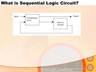
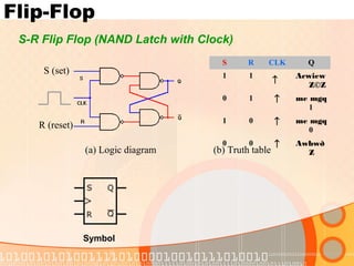
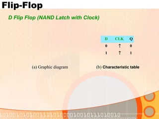
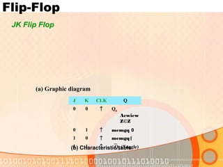
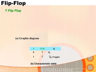
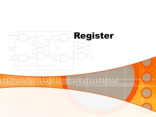
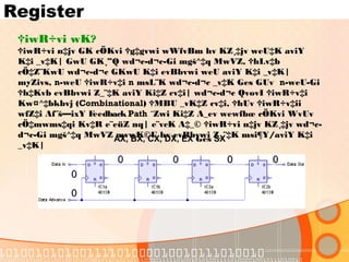
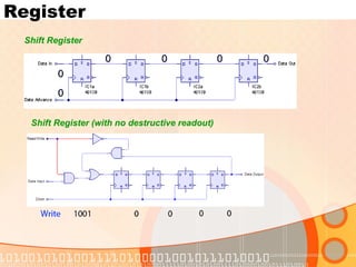
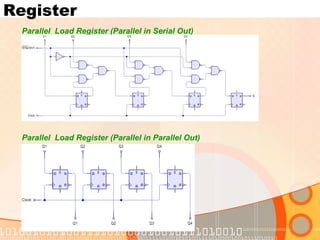
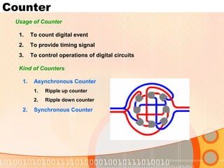
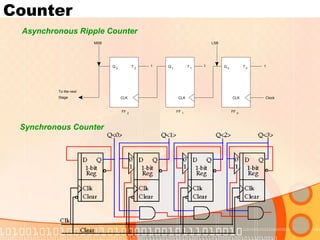
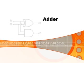
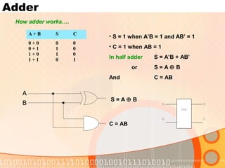
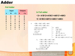
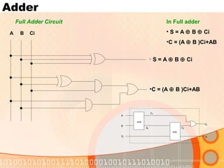
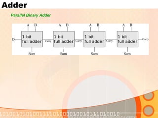
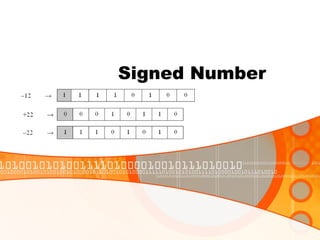
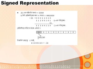
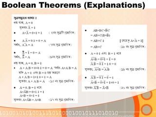
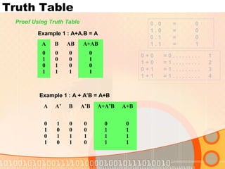
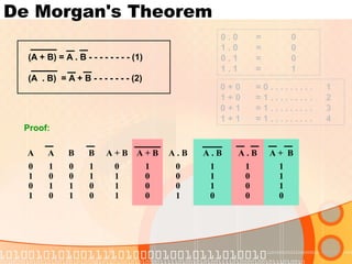
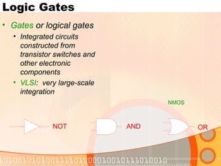
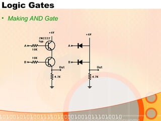
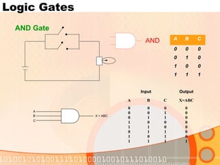
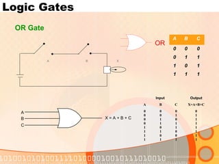
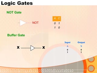
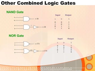
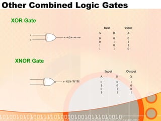
The document provides an overview of the topics covered in a digital logic design course, including Boolean algebra, logic gates, Karnaugh maps, encoders, decoders, flip-flops, registers, counters, adders, and signed number representation. The course syllabus covers basic concepts in digital logic like logic functions, logic gates, sequential logic circuits, and how to design combinational and sequential logic circuits using logic gates.


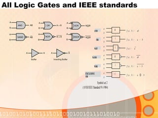
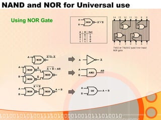
![NAND and NOR for Universal use
Using NAND Gate
[wW-giM¨v‡bi mÎvbymv‡i A.B
= A + B ]](https://image.slidesharecdn.com/digitallogic-160603031151/85/Digital-logic-25-320.jpg)