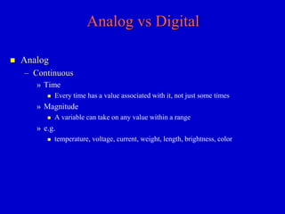
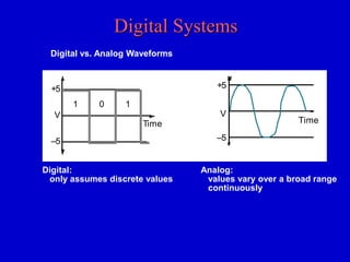
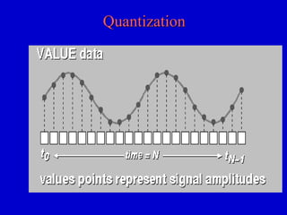
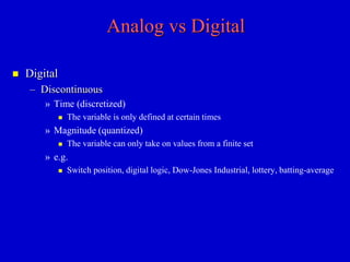
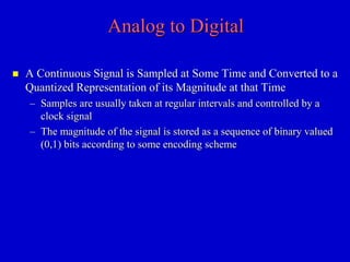
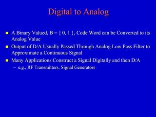
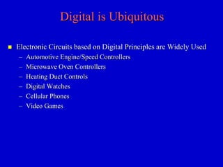
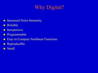
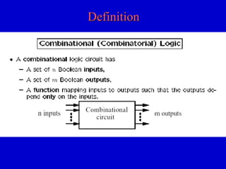
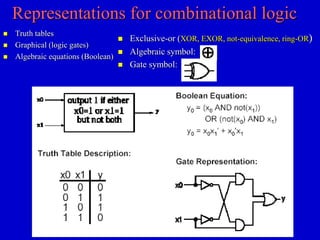
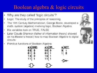
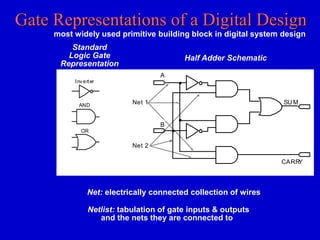
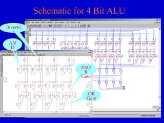
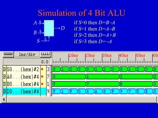
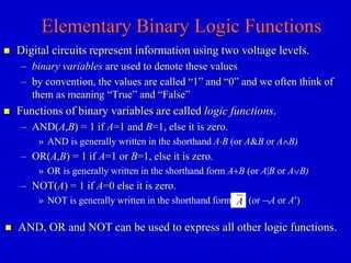
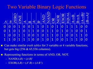
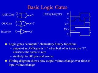
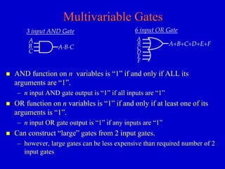
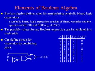
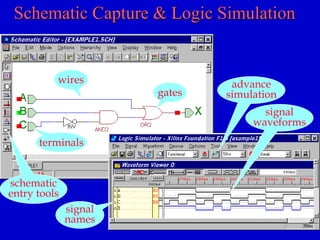
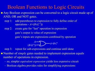
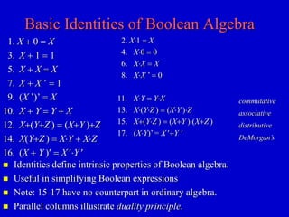
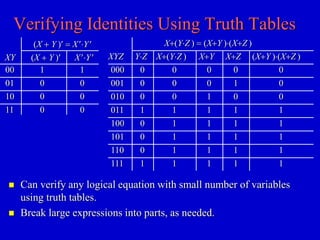
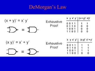
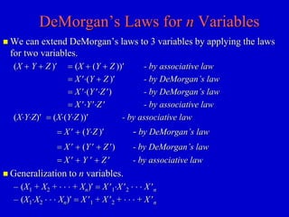
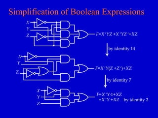
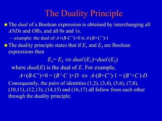
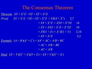
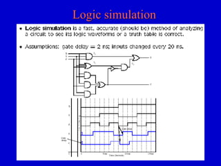
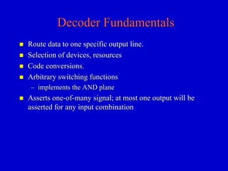
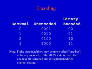
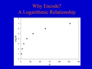
Digital Logic Circuits 
 Binary Logic and Gates 
 Logic Simulation 
 Boolean Algebra 
 NAND/NOR and XOR gates 
 Decoder fundamentals 
 Half Adder, Full Adder, Ripple Carry Adder
Analog vs Digital 
 Analog 
– Continuous 
» Time 
 Every time has a value associated with it, not just some times 
» Magnitude 
 A variable can take on any value within a range 
» e.g. 
 temperature, voltage, current, weight, length, brightness, color
Digital Systems 
Digital vs. Analog Waveforms 
Analog: 
values vary over a broad range 
continuously 
Digital: 
only assumes discrete values 
+5 
V 
–5 
T ime 
+5 
V 
–5 
1 0 1 
T ime
Quantization
Analog vs Digital 
 Digital 
– Discontinuous 
» Time (discretized) 
 The variable is only defined at certain times 
» Magnitude (quantized) 
 The variable can only take on values from a finite set 
» e.g. 
 Switch position, digital logic, Dow-Jones Industrial, lottery, batting-average
Analog to Digital 
 A Continuous Signal is Sampled at Some Time and Converted to a 
Quantized Representation of its Magnitude at that Time 
– Samples are usually taken at regular intervals and controlled by a 
clock signal 
– The magnitude of the signal is stored as a sequence of binary valued 
(0,1) bits according to some encoding scheme
Digital to Analog 
 A Binary Valued, B = { 0, 1 }, Code Word can be Converted to its 
Analog Value 
 Output of D/A Usually Passed Through Analog Low Pass Filter to 
Approximate a Continuous Signal 
 Many Applications Construct a Signal Digitally and then D/A 
– e.g., RF Transmitters, Signal Generators
Digital is Ubiquitous 
 Electronic Circuits based on Digital Principles are Widely Used 
– Automotive Engine/Speed Controllers 
– Microwave Oven Controllers 
– Heating Duct Controls 
– Digital Watches 
– Cellular Phones 
– Video Games
Why Digital? 
 Increased Noise Immunity 
 Reliable 
 Inexpensive 
 Programmable 
 Easy to Compute Nonlinear Functions 
 Reproducible 
 Small
Digital Design Process 
 Computer Aided Design Tools 
– Design entry 
– Synthesis 
– Verification and simulation 
– Physical design 
– Fabrication 
– Testing
Definition
Representations for combinational logic 
 Exclusive-or (XOR, EXOR, not-equivalence, ring-OR) 
 Algebraic symbol: 
 Gate symbol: 
 Truth tables 
 Graphical (logic gates) 
 Algebraic equations (Boolean)
Boolean algebra & logic circuits
Representations of a Digital Design 
Truth Tables 
tabulate all possible input combinations and their associated 
output values 
Example: half adder 
adds two binary digits 
to form Sum and Carry 
Example: full adder 
adds two binary digits and 
Carry in to form Sum and 
Carry Out 
A B 
0 
0 
0 
1 
1 
0 
1 
1 
Sum Carry 
0 
0 
1 
0 
1 
0 
0 
1 
NOTE: 1 plus 1 is 0 with a 
carry of 1 in binary 
A 
0 
0 
0 
0 
1 
1 
1 
1 
B 
0 
0 
1 
1 
0 
0 
1 
1 
C in 
0 
1 
0 
1 
0 
1 
0 
1 
S um 
0 
1 
1 
0 
1 
0 
0 
1 
C out 
0 
0 
0 
1 
0 
1 
1 
1
Representations of Digital Design: 
Boolean Algebra 
values: 0, 1 
variables: A, B, C, . . ., X, Y, Z 
operations: NOT, AND, OR, . . . 
NOT X is written as X 
X AND Y is written as X & Y, or sometimes X Y 
X OR Y is written as X + Y 
Deriving Boolean equations from truth tables: 
A 
0 
0 
1 
1 
B 
0 
1 
0 
1 
Sum 
0 
1 
1 
0 
Carry 
0 
0 
0 
1 
Sum = A B + A B 
Carry = A B 
OR'd together product terms 
for each truth table 
row where the function is 1 
if input variable is 0, it appears in 
complemented form; 
if 1, it appears uncomplemented
Representations of a Digital 
Design: Boolean Algebra 
A 
0 
0 
0 
0 
1 
1 
1 
1 
B 
0 
0 
1 
1 
0 
0 
1 
1 
Cin 
0 
1 
0 
1 
0 
1 
0 
1 
Sum 
0 
1 
1 
0 
1 
0 
0 
1 
Cout 
0 
0 
0 
1 
0 
1 
1 
1 
Another example: 
Sum = A B Cin + A B Cin + A B Cin + A B Cin 
Cout = A B Cin + A B Cin + A B Cin + A B Cin
Gate Representations of a Digital Design 
most widely used primitive building block in digital system design 
Standard 
Logic Gate 
Representation 
Half Adder Schematic 
Net: electrically connected collection of wires 
Netlist: tabulation of gate inputs & outputs 
and the nets they are connected to 
Inv erter 
AND 
OR 
Net 1 
Net 2 
A 
B 
SUM 
CARRY
Design methodology
Top-down vs. bottom-up design
Analysis procedures
Schematic for 4 Bit ALU 
AN 
D 
Gate 
EXO 
R 
Gate 
OR 
Gate 
Inverto 
r
Simulation of 4 Bit ALU 
if S=0 then D=B-A 
if S=1 then D=A-B 
if S=2 then D=A+B 
A 
B 
D 
4 
2 
4 
S if S=3 then D=-A
Elementary Binary Logic Functions 
 Digital circuits represent information using two voltage levels. 
– binary variables are used to denote these values 
– by convention, the values are called “1” and “0” and we often think of 
them as meaning “True” and “False” 
 Functions of binary variables are called logic functions. 
– AND(A,B) = 1 if A=1 and B=1, else it is zero. 
» AND is generally written in the shorthand AB (or A&B or AB) 
– OR(A,B) = 1 if A=1 or B=1, else it is zero. 
» OR is generally written in the shorthand form A+B (or A|B or AB) 
– NOT(A) = 1 if A=0 else it is zero. 
» NOT is generally written in the shorthand form (or A or A) A 
 AND, OR and NOT can be used to express all other logic functions.
Two Variable Binary Logic Functions 
ZERO 
0 
0 
0 
0 
A 
0 
0 
1 
1 
B 
0 
1 
0 
1 
 Can make similar truth tables for 3 variable or 4 variable functions, 
but gets big (256 & 65,536 columns). 
NOR 
1 
0 
0 
0 
A 
1 
1 
0 
0 
(BA) 
0 
1 
0 
0 
(AB) 
0 
0 
1 
0 
B 
1 
0 
1 
0 
NAND 
1 
1 
1 
0 
EXOR 
0 
1 
1 
0 
AND 
0 
0 
0 
1 
EQUAL 
1 
0 
0 
1 
AB 
1 
1 
0 
1 
B 
0 
1 
0 
1 
A 
0 
0 
1 
1 
BA 
1 
0 
1 
1 
ONE 
1 
1 
1 
1 
OR 
0 
1 
1 
1 
 Representing functions in terms of AND, OR, NOT. 
– NAND(A,B) = (AB) 
– EXOR(A,B) = (AB) + (AB )
Basic Logic Gates 
X 
Y AND Gate XY 
X+Y 
X 
Y 
OR Gate 
Inverter X X’ 
X 
Y 
XY 
X+Y 
 Logic gates “compute” elementary binary functions. 
– output of an AND gate is “1” when both of its inputs are “1”, 
otherwise the output is zero 
– similarly for OR gate and inverter 
 Timing diagram shows how output values change over time as 
input values change 
X’ 
Timing Diagram
Multivariable Gates 
3 input AND Gate 
6 input OR Gate 
 AND function on n variables is “1” if and only if ALL its 
arguments are “1”. 
– n input AND gate output is “1” if all inputs are “1” 
 OR function on n variables is “1” if and only if at least one of its 
arguments is “1”. 
– n input OR gate output is “1” if any inputs are “1” 
 Can construct “large” gates from 2 input gates. 
– however, large gates can be less expensive than required number of 2 
input gates 
ABC 
A+B+C+D+E+F 
A 
B 
C 
A 
C B 
D 
F E
Elements of Boolean Algebra 
 Boolean algebra defines rules for manipulating symbolic binary logic 
expressions. 
– a symbolic binary logic expression consists of binary variables and the 
operators AND, OR and NOT (e.g. A+BC) 
 The possible values for any Boolean expression can be tabulated in a 
truth table. 
A B C BC A+BC 
0 
0 
0 
0 
0 
0 
0 
1 
0 
0 
0 
1 
0 
1 
1 
0 
1 
1 
0 
0 
1 
0 
0 
0 
1 
1 
0 
1 
0 
1 
1 
1 
0 
1 
1 
1 
1 
1 
0 
1 
A 
B 
C 
A+BC 
 Can define circuit for 
expression by combining 
gates.
Schematic Capture & Logic Simulation 
gates 
wires 
terminals 
schematic 
entry tools 
signal 
waveforms 
signal 
names 
advance 
simulation
Boolean Functions to Logic Circuits 
 Any Boolean expression can be converted to a logic circuit made up of 
AND, OR and NOT gates. 
step 1: add parentheses to expression to fully define order of 
operations - A+(B(C)) 
step 2: create gate for “last” operation in expression 
gate’s output is value of expression 
gate’s inputs are expressions combined by operation 
A 
A+BC 
(B(C)) 
step 3: repeat for sub-expressions and continue until done 
 Number of simple gates needed to implement expression equals 
number of operations in expression. 
– so, simpler equivalent expression yields less expensive circuit 
– Boolean algebra provides rules for simplifying expressions
Basic Identities of Boolean Algebra 
1. X + 0 = X 
3. X + 1 = 1 
5. X + X = X 
7. X + X ’ = 1 
9. (X ’)’ = X 
10. X + Y = Y + X 
12. X+(Y+Z ) = (X+Y )+Z 
14. X(Y+Z ) = XY + XZ 
16. (X + Y ) = X Y  
2. X1 = X 
4. X0 = 0 
6. XX = X 
8. XX ’ = 0 
11. XY = YX 
13. X(YZ ) = (XY )Z 
15. X+(YZ ) = (X+Y )(X+Z ) 
17. (XY)’ = X +Y  
commutative 
associative 
distributive 
DeMorgan’s 
 Identities define intrinsic properties of Boolean algebra. 
 Useful in simplifying Boolean expressions 
 Note: 15-17 have no counterpart in ordinary algebra. 
 Parallel columns illustrate duality principle.
Verifying Identities Using Truth Tables 
X+(YZ ) = (X+Y )(X+Z ) 
YZ 
0 
0 
0 
1 
0 
0 
0 
1 
XYZ 
000 
001 
010 
011 
100 
101 
110 
111 
X+(YZ ) 
0 
0 
0 
1 
1 
1 
1 
1 
X+Y 
0 
0 
1 
1 
1 
1 
1 
1 
 Can verify any logical equation with small number of variables 
using truth tables. 
 Break large expressions into parts, as needed. 
X+Z 
0 
1 
0 
1 
1 
1 
1 
1 
(X+Y )(X+Z ) 
0 
0 
0 
1 
1 
1 
1 
1 
(X + Y ) = XY 
XY 
00 
01 
10 
11 
XY 
1 
0 
0 
0 
(X + Y ) 
1 
0 
0 
0
DeMorgan’s Law
DeMorgan’s Laws for n Variables 
 We can extend DeMorgan’s laws to 3 variables by applying the laws 
for two variables. 
(X + Y + Z ) = (X + (Y + Z )) - by associative law 
= X (Y + Z ) - by DeMorgan’s law 
= X (Y Z ) - by DeMorgan’s law 
= X YZ  - by associative law 
(XYZ) = (X(YZ )) - by associative law 
= X  + (YZ ) - by DeMorgan’s law 
= X  + (Y  + Z ) - by DeMorgan’s law 
= X  + Y  + Z  - by associative law 
 Generalization to n variables. 
– (X1 + X2 +    + Xn) = X 1X 2    X n 
– (X1X2    Xn) = X 1 + X 2 +    + X n
Simplification of Boolean Expressions 
F=X YZ +X YZ +XZ 
X 
Y 
Z 
X 
Y 
Z 
X 
Y 
Z 
by identity 14 
F=X Y(Z +Z )+XZ 
by identity 7 
F=X Y1+XZ 
=X Y +XZ by identity 2
The Duality Principle 
 The dual of a Boolean expression is obtained by interchanging all 
ANDs and ORs, and all 0s and 1s. 
– example: the dual of A+(BC )+0 is A(B+C )1 
 The duality principle states that if E1 and E2 are Boolean 
expressions then 
E1= E2  dual (E1)=dual (E2) 
where dual(E) is the dual of E. For example, 
A+(BC )+0 = (B C )+D  A(B+C)1 = (B +C )D 
Consequently, the pairs of identities (1,2), (3,4), (5,6), (7,8), 
(10,11), (12,13), (14,15) and (16,17) all follow from each other 
through the duality principle.
The Consensus Theorem 
Theorem. XY + X Z +YZ = XY + X Z 
Proof. XY + X Z +YZ = XY + X Z + YZ(X + X ) 2,7 
= XY + X Z + XYZ + X YZ 14 
= XY + XYZ + X Z + X YZ 10 
= XY(1 + Z ) + X Z(1 + Y ) 2,14 
= XY + X Z 3,2 
Example. (A + B )(A + C ) = AA + AC + AB + BC 
= AC + AB + BC 
= AC + AB 
Dual. (X + Y )(X  + Z )(Y + Z ) = (X + Y )(X  + Z )
Taking the Complement of a Function 
Method 1. Apply DeMorgan’s Theorem repeatedly. 
(X(YZ + YZ )) = X  + (YZ + YZ ) 
= X + (YZ)(YZ ) 
= X + (Y + Z )(Y + Z) 
Method 2. Complement literals and take dual 
(X (YZ + YZ ))= dual(X(YZ + YZ)) 
= X + (Y + Z )(Y + Z)
Sum of Products Form 
 The sum of products is one of two standard forms for Boolean 
expressions. 
sum-of-products-expression = term + term ... + term 
term = literal  literal    literal 
Example. X YZ + X Z + XY + XYZ 
 A minterm is a term that contains every variable, in either 
complemented or uncomplemented form. 
Example. in expression above, X YZ is minterm, but X Z is not 
 A sum of minterms expression is a sum of products expression in 
which every term is a minterm 
Example. X YZ + XYZ + XYZ  + XYZ is sum of minterms expression that is 
equivalent to expression above
Product of Sums Form 
 The product of sums is the second standard form for Boolean 
expressions. 
product-of-sums-expression = s-term  s-term ...  s-term 
s-term = literal + literal +  + literal 
Example. (X+Y+Z )(X+Z)(X+Y)(X+Y+Z) 
 A maxterm is a sum term that contains every variable, in 
complemented or uncomplemented form. 
Example. in exp. above, X+Y+Z is a maxterm, but X+Z is not 
 A product of maxterms expression is a product of sums expression in 
which every term is a maxterm 
Example. (X+Y+Z )(X+Y+Z)(X+Y+Z)(X+Y+Z) is product of maxterms 
expression that is equivalent to expression above
NAND and NOR Gates 
NAND Gate X 
X 
Y (XY) NOR Gate 
(X+Y) 
Y 
 In certain technologies (including CMOS), a NAND (NOR) gate is 
simpler & faster than an AND (OR) gate. 
 Consequently circuits are often constructed using NANDs and NORs 
directly, instead of ANDs and ORs. 
 Alternative gate representations makes this easier. 
= = 
= =
Exclusive Or and Odd Function 
A 
AB  
+AB 
B 
 The odd function on n variables is 1 when an odd number of its 
variables are 1. 
– odd(X,Y,Z ) = XY Z + X Y Z  + X Y Z + X Y Z = X Y Z 
– similarly for 4 or more variables 
 Parity checking circuits use the odd function to provide a simple 
integrity check to verify correctness of data. 
– any erroneous single bit change will alter value of odd function, allowing 
detection of the change 
EXOR gate 
Alternative Implementation 
A 
B 
 The EXOR function is defined by AB = AB  + AB.
Positive and Negative Logic 
 In positive logic systems, a high voltage is associated with a logic 1, 
and a low voltage with a logic 0. 
– positive logic is just one of two conventions that can be used to associate 
a logic value with a voltage 
– sometimes it is more convenient to use the opposite convention 
 In logic diagrams that use negative logic, a polarity indicator is used 
to indicate the correct logical interpretation for a signal. 
X 
Y XY X+Y 
X 
Y 
 Circuits commonly use a combination of positive and negative logic.
Analysis example
Truth tables from logic diagram
Logic simulation
Decoder Fundamentals 
 Route data to one specific output line. 
 Selection of devices, resources 
 Code conversions. 
 Arbitrary switching functions 
– implements the AND plane 
 Asserts one-of-many signal; at most one output will be 
asserted for any input combination
Encoding 
Binary 
Decimal Unencoded Encoded 
0 0001 00 
1 0010 01 
2 0100 10 
3 1000 11 
Note: Finite state machines may be unencoded ("one-hot") 
or binary encoded. If the all 0's state is used, then 
one less bit is needed and it is called modified 
one-hot coding.
Why Encode? 
A Logarithmic Relationship 
0 25 50 75 100 125 150 
N 
Log2(N) 
8 
7 
6 
5 
4 
3 
2 
1 
0
2:4 Decoder 
1 1 
1 0 
0 1 
00 
D 0 
D 1 
A 
B 
A 
B 
A 
B 
A 
B 
AND 2 
AND 2 A 
AND 2 A 
AND 2 B 
Y 
Y 
Y 
Y 
E Q 3 
E Q 2 
E Q 1 
E Q 0 
What happens when the inputs goes from 01 to 10?
2:4 Decoder with Enable 
1 1 
1 0 
0 1 
00 
D 0 
D 1 
ENABLE 
A 
B 
C 
A 
B 
C 
A 
B 
C 
A 
B 
C 
Y 
Y 
Y 
Y 
E Q 3 
E Q 2 
E Q 1 
E Q 0 
AND 3 
AND 3 A 
AND 3 A 
AND 3 B
2:1 Multiplexer 
A 
S 
B 
A 
B 
A 
B 
Y X1 
Y X2 
A 
B 
Y Y
Design synthesis procedure
Half Adder
Full Adder – with EXOR, AND and OR
Full Adder – with EXOR and NAND 
 One-bit Full Adder (FA) 
– 3 inputs: A, B, C 
– 2 outputs: S, Co 
– Truth table: 
 Schematic View: 
– cell-based approach 
A, B, C S, Co 
0, 0, 0 0, 0 
0, 0, 1 1, 0 
0, 1, 0 1, 0 
0, 1, 1 0, 1 
1, 0, 0 1, 0 
1, 0, 1 0, 1 
1, 1, 0 0, 1 
1, 1, 1 1, 1 
C S 
B 
A 
Co
Ripple Carry Adder

2dig circ

  • 1.
    Digital Logic Circuits  Binary Logic and Gates  Logic Simulation  Boolean Algebra  NAND/NOR and XOR gates  Decoder fundamentals  Half Adder, Full Adder, Ripple Carry Adder
  • 2.
    Analog vs Digital  Analog – Continuous » Time  Every time has a value associated with it, not just some times » Magnitude  A variable can take on any value within a range » e.g.  temperature, voltage, current, weight, length, brightness, color
  • 3.
    Digital Systems Digitalvs. Analog Waveforms Analog: values vary over a broad range continuously Digital: only assumes discrete values +5 V –5 T ime +5 V –5 1 0 1 T ime
  • 4.
  • 5.
    Analog vs Digital  Digital – Discontinuous » Time (discretized)  The variable is only defined at certain times » Magnitude (quantized)  The variable can only take on values from a finite set » e.g.  Switch position, digital logic, Dow-Jones Industrial, lottery, batting-average
  • 6.
    Analog to Digital  A Continuous Signal is Sampled at Some Time and Converted to a Quantized Representation of its Magnitude at that Time – Samples are usually taken at regular intervals and controlled by a clock signal – The magnitude of the signal is stored as a sequence of binary valued (0,1) bits according to some encoding scheme
  • 7.
    Digital to Analog  A Binary Valued, B = { 0, 1 }, Code Word can be Converted to its Analog Value  Output of D/A Usually Passed Through Analog Low Pass Filter to Approximate a Continuous Signal  Many Applications Construct a Signal Digitally and then D/A – e.g., RF Transmitters, Signal Generators
  • 8.
    Digital is Ubiquitous  Electronic Circuits based on Digital Principles are Widely Used – Automotive Engine/Speed Controllers – Microwave Oven Controllers – Heating Duct Controls – Digital Watches – Cellular Phones – Video Games
  • 9.
    Why Digital? Increased Noise Immunity  Reliable  Inexpensive  Programmable  Easy to Compute Nonlinear Functions  Reproducible  Small
  • 10.
    Digital Design Process  Computer Aided Design Tools – Design entry – Synthesis – Verification and simulation – Physical design – Fabrication – Testing
  • 11.
  • 12.
    Representations for combinationallogic  Exclusive-or (XOR, EXOR, not-equivalence, ring-OR)  Algebraic symbol:  Gate symbol:  Truth tables  Graphical (logic gates)  Algebraic equations (Boolean)
  • 13.
    Boolean algebra &logic circuits
  • 14.
    Representations of aDigital Design Truth Tables tabulate all possible input combinations and their associated output values Example: half adder adds two binary digits to form Sum and Carry Example: full adder adds two binary digits and Carry in to form Sum and Carry Out A B 0 0 0 1 1 0 1 1 Sum Carry 0 0 1 0 1 0 0 1 NOTE: 1 plus 1 is 0 with a carry of 1 in binary A 0 0 0 0 1 1 1 1 B 0 0 1 1 0 0 1 1 C in 0 1 0 1 0 1 0 1 S um 0 1 1 0 1 0 0 1 C out 0 0 0 1 0 1 1 1
  • 15.
    Representations of DigitalDesign: Boolean Algebra values: 0, 1 variables: A, B, C, . . ., X, Y, Z operations: NOT, AND, OR, . . . NOT X is written as X X AND Y is written as X & Y, or sometimes X Y X OR Y is written as X + Y Deriving Boolean equations from truth tables: A 0 0 1 1 B 0 1 0 1 Sum 0 1 1 0 Carry 0 0 0 1 Sum = A B + A B Carry = A B OR'd together product terms for each truth table row where the function is 1 if input variable is 0, it appears in complemented form; if 1, it appears uncomplemented
  • 16.
    Representations of aDigital Design: Boolean Algebra A 0 0 0 0 1 1 1 1 B 0 0 1 1 0 0 1 1 Cin 0 1 0 1 0 1 0 1 Sum 0 1 1 0 1 0 0 1 Cout 0 0 0 1 0 1 1 1 Another example: Sum = A B Cin + A B Cin + A B Cin + A B Cin Cout = A B Cin + A B Cin + A B Cin + A B Cin
  • 17.
    Gate Representations ofa Digital Design most widely used primitive building block in digital system design Standard Logic Gate Representation Half Adder Schematic Net: electrically connected collection of wires Netlist: tabulation of gate inputs & outputs and the nets they are connected to Inv erter AND OR Net 1 Net 2 A B SUM CARRY
  • 18.
  • 19.
  • 20.
  • 21.
    Schematic for 4Bit ALU AN D Gate EXO R Gate OR Gate Inverto r
  • 22.
    Simulation of 4Bit ALU if S=0 then D=B-A if S=1 then D=A-B if S=2 then D=A+B A B D 4 2 4 S if S=3 then D=-A
  • 23.
    Elementary Binary LogicFunctions  Digital circuits represent information using two voltage levels. – binary variables are used to denote these values – by convention, the values are called “1” and “0” and we often think of them as meaning “True” and “False”  Functions of binary variables are called logic functions. – AND(A,B) = 1 if A=1 and B=1, else it is zero. » AND is generally written in the shorthand AB (or A&B or AB) – OR(A,B) = 1 if A=1 or B=1, else it is zero. » OR is generally written in the shorthand form A+B (or A|B or AB) – NOT(A) = 1 if A=0 else it is zero. » NOT is generally written in the shorthand form (or A or A) A  AND, OR and NOT can be used to express all other logic functions.
  • 24.
    Two Variable BinaryLogic Functions ZERO 0 0 0 0 A 0 0 1 1 B 0 1 0 1  Can make similar truth tables for 3 variable or 4 variable functions, but gets big (256 & 65,536 columns). NOR 1 0 0 0 A 1 1 0 0 (BA) 0 1 0 0 (AB) 0 0 1 0 B 1 0 1 0 NAND 1 1 1 0 EXOR 0 1 1 0 AND 0 0 0 1 EQUAL 1 0 0 1 AB 1 1 0 1 B 0 1 0 1 A 0 0 1 1 BA 1 0 1 1 ONE 1 1 1 1 OR 0 1 1 1  Representing functions in terms of AND, OR, NOT. – NAND(A,B) = (AB) – EXOR(A,B) = (AB) + (AB )
  • 25.
    Basic Logic Gates X Y AND Gate XY X+Y X Y OR Gate Inverter X X’ X Y XY X+Y  Logic gates “compute” elementary binary functions. – output of an AND gate is “1” when both of its inputs are “1”, otherwise the output is zero – similarly for OR gate and inverter  Timing diagram shows how output values change over time as input values change X’ Timing Diagram
  • 26.
    Multivariable Gates 3input AND Gate 6 input OR Gate  AND function on n variables is “1” if and only if ALL its arguments are “1”. – n input AND gate output is “1” if all inputs are “1”  OR function on n variables is “1” if and only if at least one of its arguments is “1”. – n input OR gate output is “1” if any inputs are “1”  Can construct “large” gates from 2 input gates. – however, large gates can be less expensive than required number of 2 input gates ABC A+B+C+D+E+F A B C A C B D F E
  • 27.
    Elements of BooleanAlgebra  Boolean algebra defines rules for manipulating symbolic binary logic expressions. – a symbolic binary logic expression consists of binary variables and the operators AND, OR and NOT (e.g. A+BC)  The possible values for any Boolean expression can be tabulated in a truth table. A B C BC A+BC 0 0 0 0 0 0 0 1 0 0 0 1 0 1 1 0 1 1 0 0 1 0 0 0 1 1 0 1 0 1 1 1 0 1 1 1 1 1 0 1 A B C A+BC  Can define circuit for expression by combining gates.
  • 28.
    Schematic Capture &Logic Simulation gates wires terminals schematic entry tools signal waveforms signal names advance simulation
  • 29.
    Boolean Functions toLogic Circuits  Any Boolean expression can be converted to a logic circuit made up of AND, OR and NOT gates. step 1: add parentheses to expression to fully define order of operations - A+(B(C)) step 2: create gate for “last” operation in expression gate’s output is value of expression gate’s inputs are expressions combined by operation A A+BC (B(C)) step 3: repeat for sub-expressions and continue until done  Number of simple gates needed to implement expression equals number of operations in expression. – so, simpler equivalent expression yields less expensive circuit – Boolean algebra provides rules for simplifying expressions
  • 30.
    Basic Identities ofBoolean Algebra 1. X + 0 = X 3. X + 1 = 1 5. X + X = X 7. X + X ’ = 1 9. (X ’)’ = X 10. X + Y = Y + X 12. X+(Y+Z ) = (X+Y )+Z 14. X(Y+Z ) = XY + XZ 16. (X + Y ) = X Y  2. X1 = X 4. X0 = 0 6. XX = X 8. XX ’ = 0 11. XY = YX 13. X(YZ ) = (XY )Z 15. X+(YZ ) = (X+Y )(X+Z ) 17. (XY)’ = X +Y  commutative associative distributive DeMorgan’s  Identities define intrinsic properties of Boolean algebra.  Useful in simplifying Boolean expressions  Note: 15-17 have no counterpart in ordinary algebra.  Parallel columns illustrate duality principle.
  • 31.
    Verifying Identities UsingTruth Tables X+(YZ ) = (X+Y )(X+Z ) YZ 0 0 0 1 0 0 0 1 XYZ 000 001 010 011 100 101 110 111 X+(YZ ) 0 0 0 1 1 1 1 1 X+Y 0 0 1 1 1 1 1 1  Can verify any logical equation with small number of variables using truth tables.  Break large expressions into parts, as needed. X+Z 0 1 0 1 1 1 1 1 (X+Y )(X+Z ) 0 0 0 1 1 1 1 1 (X + Y ) = XY XY 00 01 10 11 XY 1 0 0 0 (X + Y ) 1 0 0 0
  • 32.
  • 33.
    DeMorgan’s Laws forn Variables  We can extend DeMorgan’s laws to 3 variables by applying the laws for two variables. (X + Y + Z ) = (X + (Y + Z )) - by associative law = X (Y + Z ) - by DeMorgan’s law = X (Y Z ) - by DeMorgan’s law = X YZ  - by associative law (XYZ) = (X(YZ )) - by associative law = X  + (YZ ) - by DeMorgan’s law = X  + (Y  + Z ) - by DeMorgan’s law = X  + Y  + Z  - by associative law  Generalization to n variables. – (X1 + X2 +    + Xn) = X 1X 2    X n – (X1X2    Xn) = X 1 + X 2 +    + X n
  • 34.
    Simplification of BooleanExpressions F=X YZ +X YZ +XZ X Y Z X Y Z X Y Z by identity 14 F=X Y(Z +Z )+XZ by identity 7 F=X Y1+XZ =X Y +XZ by identity 2
  • 35.
    The Duality Principle  The dual of a Boolean expression is obtained by interchanging all ANDs and ORs, and all 0s and 1s. – example: the dual of A+(BC )+0 is A(B+C )1  The duality principle states that if E1 and E2 are Boolean expressions then E1= E2  dual (E1)=dual (E2) where dual(E) is the dual of E. For example, A+(BC )+0 = (B C )+D  A(B+C)1 = (B +C )D Consequently, the pairs of identities (1,2), (3,4), (5,6), (7,8), (10,11), (12,13), (14,15) and (16,17) all follow from each other through the duality principle.
  • 36.
    The Consensus Theorem Theorem. XY + X Z +YZ = XY + X Z Proof. XY + X Z +YZ = XY + X Z + YZ(X + X ) 2,7 = XY + X Z + XYZ + X YZ 14 = XY + XYZ + X Z + X YZ 10 = XY(1 + Z ) + X Z(1 + Y ) 2,14 = XY + X Z 3,2 Example. (A + B )(A + C ) = AA + AC + AB + BC = AC + AB + BC = AC + AB Dual. (X + Y )(X  + Z )(Y + Z ) = (X + Y )(X  + Z )
  • 37.
    Taking the Complementof a Function Method 1. Apply DeMorgan’s Theorem repeatedly. (X(YZ + YZ )) = X  + (YZ + YZ ) = X + (YZ)(YZ ) = X + (Y + Z )(Y + Z) Method 2. Complement literals and take dual (X (YZ + YZ ))= dual(X(YZ + YZ)) = X + (Y + Z )(Y + Z)
  • 38.
    Sum of ProductsForm  The sum of products is one of two standard forms for Boolean expressions. sum-of-products-expression = term + term ... + term term = literal  literal    literal Example. X YZ + X Z + XY + XYZ  A minterm is a term that contains every variable, in either complemented or uncomplemented form. Example. in expression above, X YZ is minterm, but X Z is not  A sum of minterms expression is a sum of products expression in which every term is a minterm Example. X YZ + XYZ + XYZ  + XYZ is sum of minterms expression that is equivalent to expression above
  • 39.
    Product of SumsForm  The product of sums is the second standard form for Boolean expressions. product-of-sums-expression = s-term  s-term ...  s-term s-term = literal + literal +  + literal Example. (X+Y+Z )(X+Z)(X+Y)(X+Y+Z)  A maxterm is a sum term that contains every variable, in complemented or uncomplemented form. Example. in exp. above, X+Y+Z is a maxterm, but X+Z is not  A product of maxterms expression is a product of sums expression in which every term is a maxterm Example. (X+Y+Z )(X+Y+Z)(X+Y+Z)(X+Y+Z) is product of maxterms expression that is equivalent to expression above
  • 40.
    NAND and NORGates NAND Gate X X Y (XY) NOR Gate (X+Y) Y  In certain technologies (including CMOS), a NAND (NOR) gate is simpler & faster than an AND (OR) gate.  Consequently circuits are often constructed using NANDs and NORs directly, instead of ANDs and ORs.  Alternative gate representations makes this easier. = = = =
  • 41.
    Exclusive Or andOdd Function A AB  +AB B  The odd function on n variables is 1 when an odd number of its variables are 1. – odd(X,Y,Z ) = XY Z + X Y Z  + X Y Z + X Y Z = X Y Z – similarly for 4 or more variables  Parity checking circuits use the odd function to provide a simple integrity check to verify correctness of data. – any erroneous single bit change will alter value of odd function, allowing detection of the change EXOR gate Alternative Implementation A B  The EXOR function is defined by AB = AB  + AB.
  • 42.
    Positive and NegativeLogic  In positive logic systems, a high voltage is associated with a logic 1, and a low voltage with a logic 0. – positive logic is just one of two conventions that can be used to associate a logic value with a voltage – sometimes it is more convenient to use the opposite convention  In logic diagrams that use negative logic, a polarity indicator is used to indicate the correct logical interpretation for a signal. X Y XY X+Y X Y  Circuits commonly use a combination of positive and negative logic.
  • 43.
  • 44.
    Truth tables fromlogic diagram
  • 45.
  • 46.
    Decoder Fundamentals Route data to one specific output line.  Selection of devices, resources  Code conversions.  Arbitrary switching functions – implements the AND plane  Asserts one-of-many signal; at most one output will be asserted for any input combination
  • 47.
    Encoding Binary DecimalUnencoded Encoded 0 0001 00 1 0010 01 2 0100 10 3 1000 11 Note: Finite state machines may be unencoded ("one-hot") or binary encoded. If the all 0's state is used, then one less bit is needed and it is called modified one-hot coding.
  • 48.
    Why Encode? ALogarithmic Relationship 0 25 50 75 100 125 150 N Log2(N) 8 7 6 5 4 3 2 1 0
  • 49.
    2:4 Decoder 11 1 0 0 1 00 D 0 D 1 A B A B A B A B AND 2 AND 2 A AND 2 A AND 2 B Y Y Y Y E Q 3 E Q 2 E Q 1 E Q 0 What happens when the inputs goes from 01 to 10?
  • 50.
    2:4 Decoder withEnable 1 1 1 0 0 1 00 D 0 D 1 ENABLE A B C A B C A B C A B C Y Y Y Y E Q 3 E Q 2 E Q 1 E Q 0 AND 3 AND 3 A AND 3 A AND 3 B
  • 51.
    2:1 Multiplexer A S B A B A B Y X1 Y X2 A B Y Y
  • 52.
  • 53.
  • 54.
    Full Adder –with EXOR, AND and OR
  • 55.
    Full Adder –with EXOR and NAND  One-bit Full Adder (FA) – 3 inputs: A, B, C – 2 outputs: S, Co – Truth table:  Schematic View: – cell-based approach A, B, C S, Co 0, 0, 0 0, 0 0, 0, 1 1, 0 0, 1, 0 1, 0 0, 1, 1 0, 1 1, 0, 0 1, 0 1, 0, 1 0, 1 1, 1, 0 0, 1 1, 1, 1 1, 1 C S B A Co
  • 56.