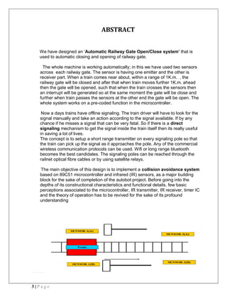
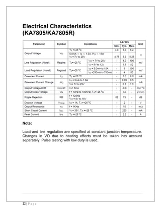
1 | P a g e
Student’s Declaration
I/We hereby declare that the work being presented in this report entitled
“AUTOMATIC BARRIER SYSTEM, DIRECT SIGNALLING
AND COLLISION CONTROL FOR TRAINS” is an authentic record of
my / our own work carried out under the supervision of Mrs. “K.NISHA”
The matter embodied in this report has not been submitted by me / us for the award
of any other degree.
Date:
Signature of student Signature of student
(Name: AFZAL ISHTIAQ USMANI) (Name: AMIT KUMAR)
Roll no :0903221006 Roll no :0903221011
Department: EEE Department :EEE
Signature of student Signature of student
(Name: AVNEESH TYAGI) (Name: ABHINAV DUBEY)
Roll no :09032210038 Roll no :0903221003
Department: EEE Department :EEE
This is to certify that the above statement made by the candidate(s) is correct to the
best of my knowledge.
Signature of Supervisor
(Mrs. K.Nisha) :
(Designation)
Signature of Head of Department
Prof. (Dr.) Amul Kumar Agrawal
Department of ELECTRICAL & ELECTRONICS ENGINEERING
Date............................
2 | P a g e
ACKNOWLEDGEMENT
We are very happy on the completion of the mini Project
‘Automatic Railway Gate Open/Close System’ at Academy Of
Business and Engineering Sciences, Ghaziabad, for which I Would
like to thank Mrs K.nisha ,under whose visionary enlightenment I
was able to complete this report. I would also like to acknowledge
the help and support by Respected HOD sir Mr.Amul kr.
Agarwal who spared his precious time for the sake of this report.
Making this project without the help of my
teammates wouldn’t had been possible so we would also like to
thank each other for that.
We would also like to thank our college for the
help and resources they have provided to us without which our
dream to complete this project wouldn’t had been completed
Date:
Signature of student Signature of student
(Name: AFZAL ISHTIAQ USMANI) (Name: AMIT KUMAR)
Roll no :0903221006 Roll no :0903221011
Department: EEE Department :EEE
Signature of student Signature of student
(Name: AVNEESH TYAGI) (Name: ABHINAV
DUBEY)
Roll no :09032210038 Roll no :0903221003
Department: EEE Department :EEE
3 | P a g e
ABSTRACT
We have designed an ‘Automatic Railway Gate Open/Close system’ that is
used to automatic closing and opening of railway gate.
The whole machine is working automatically; in this we have used two sensors
across each railway gate. The sensor is having one emitter and the other is
receiver part. When a train comes near about, within a range of 1K.m. , the
railway gate will be closed and after that when train moves further 1K.m. ahead
then the gate will be opened, such that when the train crosses the sensors then
an interrupt will be generated so at the same moment the gate will be close and
further when train passes the sensors at the other end the gate will be open. The
whole system works on a pre-coded function in the microcontroller.
Now a days trains have offline signaling. The train driver will have to look for the
signal manually and take an action according to the signal available. If by any
chance if he misses a signal that can be very fatal. So if there is a direct
signaling mechanism to get the signal inside the train itself then its really useful
in saving a lot of lives.
The concept is to setup a short range transmitter on every signaling pole so that
the train can pick up the signal as it approaches the pole. Any of the commercial
wireless communication protocols can be used. Wifi or long range bluetooth
becomes the best candidates. The signaling poles can be reached through the
railnet optical fibre cables or by using satellite relays.
The main objective of this design is to implement a collision avoidance system
based on 89C51 microcontroller and infrared (IR) sensors, as a major building
block for the sake of completion of the autobot project. Before going into the
depths of its constructional characteristics and functional details, few basic
perceptions associated to the microcontroller, IR transmitter, IR receiver, timer IC
and the theory of operation has to be revived for the sake of its profound
understanding
4 | P a g e
Table Of Contents
CHAPTER NO. CHAPTER NAME PAGE NO
1 Basic concepts 5-6
2. Hardware used 7
3. 89S52 µC 8-15
4. L293D IC 16-19
5. L7805IC 20-22
6. Simple 5V
supply for direct
current
23-24
7. Relay 25
8. 12 E encoder 26-31
9. 12 D decoder 32-36
10. Block diagrams 37-42
11. IR sensor based
object
orientation and
collision control
for trains
43-47
Conclusion 48
Appendix 49-53
Reference 54
5 | P a g e
CHAPTER 1
Basic concepts
1.1 INFRARED BASICS
As illustrated in Figure 1.1, Infrared is an energy radiation with a frequency below our eyes
sensitivity level, thus can’t be seen with naked eyes. Infrared waves can be easily generated
and does not undergo electromagnetic interference, so it can be used abundantly for
communication and control oriented operations. There are some potentially constraining
sources of infrared emission also, such as sunlight (a major source of infrared), or any other
heat radiating body in the vicinity that can cause severe interference to infrared energy levels.
Despite of the presence of these restraining aspects Infrared wave finds hand full of
applications in the field of electronics and can easily be opted as a far better means to
implement the line of sight collision detection scheme over the existing alternatives.
Figure 1.1: Light Spectrum
1.2 OBJECT DETECTIONAND COLLISION AVOIDANCE
The principle of object detection is carried out by infrared waves radiated from IR light
emitting diodes (LEDs) and monitoring the reflected light by means of IR sensors to
detect the presence of any obstacle on the line of sight path. Thereafter, depending
upon it, the microcontroller makes a befitting decision to avoid the collision. The
concept of obstacle detection and collision avoidance is depicted in Figure 1.2.
Figure 1.2: Principle of Operation
Here the phrase ‘befitting decision’ means to make the robotic cart to take a turn towards the
correct direction or to stall its motion and to take a ‘U-turn’ depending upon the obstacle’s
dimensions and its location in the path.
6 | P a g e
1.3 IR LED
TSAL6200 by VISHAY Semiconductors is a high efficiency infrared emitting diode in
Gallium Aluminum Arsenide (GaAlAs) on Gallium Arsenide (GaAs) technology, molded in
clear, blue-grey tinted plastic packages. These IR LEDs provide high radiant at a low forward
voltage. They emit IR waves of 760 nm wavelength.
Figure 1.3: TSAL6200 IR LED
1.4 IR SENSOR
TSOP1738 by VISHAY Semiconductors is an ambient light immune low power consumptive
photo detector and pre amplifier embedded in the single epoxy package for IR wave reception
and demodulation. The pinnacle of this IR sensor is that the demodulated output signal can
directly be fed to the controller unit as it supports both TTL and CMOS logics reducing the
requirement of additional hardware for decoding. This sensor can demodulate IR wave of
frequency 38 kHz accurately. Pin 1 is GND, Pin 2 is Vs and Pin 3 is OUT.
Figure 1.4: TSOP1738 IR Sensor
7 | P a g e
CHAPTER 2
Hardware used
 89S52 Microcontroller
 L293D IC
 LM7805 Voltage Regulator
 Buzzer
 Crystal Oscillator
 Resistor
 Switch
 Capacitor
 LED
 Diode
 DC Motor
 Transformer
 12 D decoder
 12 E encoder.
8 | P a g e
CHAPTER 3
89S52 MICROCONTROLLER
Features
• Compatible with MCS®-51 Products
• 8K Bytes of In-System Programmable (ISP) Flash Memory
– Endurance: 1000 Write/Erase Cycles
• 4.0V to 5.5V Operating Range
• Fully Static Operation: 0 Hz to 33 MHz
• Three-level Program Memory Lock
• 256 x 8-bit Internal RAM
• 32 Programmable I/O Lines
• Three 16-bit Timer/Counters
• Eight Interrupt Sources
• Full Duplex UART Serial Channel
• Low-power Idle and Power-down Modes
• Interrupt Recovery from Power-down Mode
• Watchdog Timer
• Dual Data Pointer
• Power-off Flag
• Fast Programming Time
• Flexible ISP Programming (Byte and Page Mode)
• Green (Pb/Halide-free) Packaging Option
9 | P a g e
Description
The AT89S52 is a low-power, high-performance CMOS 8-bit microcontroller with 8K
bytes of in-system programmable Flash memory. The device is manufactured using
Atmel’s high-density nonvolatile memory technology and is compatible with the
industry-standard 80C51 instruction set and pinout. The on-chip Flash allows the
program memory to be reprogrammed in-system or by a conventional nonvolatile
memory programmer. By combining a versatile 8-bit CPU with in-system
programmable Flash on a monolithic chip, the Atmel AT89S52 is a powerful
microcontroller which provides a highly-flexible and cost-effective solution to many
embedded control applications. The AT89S52 provides the following standard
features: 8K bytes of Flash, 256 bytes of RAM, 32 I/O lines, Watchdog timer, two
data pointers, three 16-bit timer/counters, a six-vector two-level interrupt architecture,
a full duplex serial port, on-chip oscillator, and clock circuitry. In addition, the
AT89S52 is designed with static logic for operation down to zero frequency and
supports two software selectable power saving modes. The Idle Mode stops the CPU
while allowing the RAM, timer/counters, serial port, and interrupt system to continue
functioning. The Power-down mode saves the RAM contents but freezes the
oscillator, disabling all other chip functions until the next interrupt or hardware reset.
Pin Configurations
40 lead PDIP-
10 | P a g e
Block Diagram
11 | P a g e
Pin Description
VCC - Supply voltage.
GND - Ground.
Port 0 is an 8-bit open drain bidirectional I/O port. As an output port, each pin can
sink eight TTL inputs. When 1s are written to port 0 pins, the pins can be used as
high-impedance inputs. Port 0 can also be configured to be the multiplexed low-order
address/data bus during accesses to external program and data memory. In this
mode, P0 has internal pull-ups. Port 0 also receives the code bytes during Flash
programming and outputs the code bytes during program verification. External pull-
ups are required during program verification.
Port 1
Port 1 is an 8-bit bidirectional I/O port with internal pull-ups. The Port 1 output buffers
can sink/source four TTL inputs. When 1s are written to Port 1 pins, they are pulled
high by the internal pull-ups and can be used as inputs. As inputs, Port 1 pins that are
externally being pulled low will source current (IIL) because of the internal pull-ups. In
addition, P1.0 and P1.1 can be configured to be the timer/counter 2 external count
input (P1.0/T2) and the timer/counter 2 trigger input (P1.1/T2EX), respectively, as
shown in the following table. Port 1 also receives the low-order address bytes during
Flash programming and verification.
Port Pin Alternate Functions
P1.0 T2 (external count input to Timer/Counter 2), clock-out
P1.1 T2EX (Timer/Counter 2 capture/reload trigger and direction control)
P1.5 MOSI (used for In-System Programming)
P1.6 MISO (used for In-System Programming)
P1.7 SCK (used for In-System Programming
Port 2
Port 2 is an 8-bit bidirectional I/O port with internal pull-ups. The Port 2 output buffers
can sink/source four TTL inputs. When 1s are written to Port 2 pins, they are pulled
high by the internal pull-ups and can be used as inputs. As inputs, Port 2 pins that are
externally being pulled low will source current (IIL) because of the internal pull-ups.
Port 2 emits the high-order address byte during fetches from external program
memory and during accesses to external data memory that use 16-bit addresses
(MOVX @ DPTR). In this application, Port 2 uses strong internal pull-ups when
emitting 1s. During accesses to external data memory that use 8-bit addresses
12 | P a g e
(MOVX @ RI), Port 2 emits the contents of the P2 Special Function Register. Port 2
also receives the high-order address bits and some control signals during Flash
programming and verification.
Port 3
Port 3 is an 8-bit bidirectional I/O port with internal pull-ups. The Port 3 output buffers
can sink/source four TTL inputs. When 1s are written to Port 3 pins, they are pulled
high by the internal pull-ups and can be used as inputs. As inputs, Port 3 pins that are
externally being pulled low will source current (IIL) because of the pull-ups. Port 3
receives some control signals for Flash programming and verification. Port 3 also
serves the functions of various special features of the AT89S52, as shown in the
following table.
Port Pin Alternate Functions
P3.0 RXD (serial input port)
P3.1 TXD (serial output port)
P3.2 INT0 (external interrupt 0)
P3.3 INT1 (external interrupt 1)
P3.4 T0 (timer 0 external input)
P3.5 T1 (timer 1 external input)
P3.6 WR (external data memory write strobe)
P3.7 RD (external data memory read strobe)
RST
Reset input. A high on this pin for two machine cycles while the oscillator is running
resets the device. This pin drives high for 98 oscillator periods after the Watchdog
times out. The DISRTO bit in SFR AUXR (address 8EH) can be used to disable this
feature. In the default state of bit DISRTO, the RESET HIGH out feature is enabled.
ALE/PROG
Address Latch Enable (ALE) is an output pulse for latching the low byte of the
address during accesses to external memory. This pin is also the program pulse input
(PROG) during Flash programming. In normal operation, ALE is emitted at a constant
rate of 1/6 the oscillator frequency and may be used for external timing or clocking
purposes. Note, however, that one ALE pulse is skipped during each access to
external data memory. If desired, ALE operation can be disabled by setting bit 0 of
SFR location 8EH. With the bit set, ALE is active only during a MOVX or MOVC
instruction. Otherwise, the pin is weakly pulled high. Setting the ALE-disable bit has
no effect if the microcontroller is in external execution mode.
PSEN
Program Store Enable (PSEN) is the read strobe to external program memory. When
the AT89S52 is executing code from external program memory, PSEN is activated
13 | P a g e
twice each machine cycle, except that two PSEN activations are skipped during each
access to external data memory.
EA/VPP
External Access Enable. EA must be strapped to GND in order to enable the device
to fetch code from external program memory locations starting at 0000H up to
FFFFH. Note, however, that if lock bit 1 is programmed, EA will be internally latched
on reset. EA should be strapped to VCC for internal program executions. This pin
also receives the 12-volt programming enable voltage (VPP) during Flash
programming.
XTAL1
Input to the inverting oscillator amplifier and input to the internal clock operating
circuit.
XTAL2
Output from the inverting oscillator amplifier.
Oscillator Characteristics
XTAL1 and XTAL2 are the input and output, respectively, of an inverting amplifier that
can be configured for use as an on-chip oscillator, as shown in Figure below. Either a
quartz crystal or ceramic resonator may be used. To drive the device from an
external clock source, XTAL2 should be left unconnected while XTAL1 is driven, as
shown in Figure below. There are no requirements on the duty cycle of the external
clock signal, since the input to the internal clocking circuitry is through a divide-by-two
flip-flop, but minimum and maximum voltage high and low time specifications must be
observed.
14 | P a g e
15 | P a g e
Basic
Diagram
Absolute Maximum Ratings*
16 | P a g e
CHAPTER 4
L293D IC
 600mA OUTPUT CURRENT CAPABILITY PER CHANNEL
 1.2A PEAK OUTPUT CURRENT (non repetitive) PER CHANNEL
 ENABLE FACILITY
 OVERTEMPERATURE PROTECTION
 LOGICAL "0" INPUT VOLTAGE UP TO 1.5 V (HIGH NOISE IMMUNITY)
 I NTERNAL CLAMP DIODES
DESCRIPTION
The device is a monolithic integrated high voltage,high current four channel driver
designed to accept standard DTL or TTL logic levels and drive inductive loads ( such
as relay solenoids, DC and stepping motors) and switching power transistors.
To simplify use as two bridges each pair of channels is equipped with an enable
input. A separate supply input is provided for the logic, allowing operation at a lower
voltage and internal clamp diodes are included.
This device is suitable for use in switching applications at frequency up to 5 kHz.
The l293d is assembled in a 16 lead plastic package which has 4 center pins
connected to gather and used for heatsinking
17 | P a g e
18 | P a g e
19 | P a g e
20 | P a g e
CHAPTER 5
L 7805 VOLTAGE REGULATOR
Features
• Output Current up to 1A
• Output Voltages of 5, 6, 8, 9, 10, 12, 15, 18, 24V
• Thermal Overload Protection
• Short Circuit Protection
• Output Transistor Safe Operating Area Protection
Description
The KA78XX/KA78XXA series of three-terminal positive regulator are
available in the TO-220/D-PAK package and with several fixed output
voltages, making them useful in a wide range of applications. Each type
employs internal current limiting, thermal shut down and safe operating
area protection, making it essentially indestructible. If adequate heat
sinking is provided, they can deliver over 1A output current. Although
designed primarily as fixed voltage regulators, these devices can be used
with external components to obtain adjustable voltages and currents.
TO-220 D-PAK
1 1
1. Input 2. GND 3. Output
21 | P a g e
Internal Block Diagram
Absolute Maximum Ratings
22 | P a g e
Electrical Characteristics
(KA7805/KA7805R)
Note:
Load and line regulation are specified at constant junction temperature.
Changes in VO due to heating effects must be taken into account
separately. Pulse testing with low duty is used.
23 | P a g e
CHAPTER 6
Simple 5V power supply for digital circuits
Summary of circuit features
 Brief description of operation: Gives out well regulated +5V output, output current
capability of 100 mA
 Circuit protection: Built-in overheating protection shuts down output when
regulator IC gets too hot
 Circuit complexity: Very simple and easy to build
 Circuit performance: Very stable +5V output voltage, reliable operation
 Availability of components: Easy to get, uses only very common basic
components
 Design testing: Based on datasheet example circuit, I have used this circuit
succesfully as part of many electronics projects
 Applications: Part of electronics devices, small laboratory power supply
 Power supply voltage: Unreglated DC 8-18V power supply
 Power supply current: Needed output current + 5 mA
 Component costs: Few dollars for the electronics components + the input
transformer cost
Circuit description
This circuit is a small +5V power supply, which is useful when experimenting with
digital electronics. Small inexpensive wall tranformers with variable output voltage are
available from any electronics shop and supermarket. Those transformers are easily
available, but usually their voltage regulation is very poor, which makes then not very
usable for digital circuit experimenter unless a better regulation can be achieved in
some way. The following circuit is the answer to the problem.
This circuit can give +5V output at about 150 mA current, but it can be increased to 1
A when good cooling is added to 7805 regulator chip. The circuit has over overload
and terminal protection.
Circuit diagram of the power supply.
24 | P a g e
The capacitors must have enough high voltage rating to safely handle the input
voltage feed to circuit. The circuit is very easy to build for example into a piece of
Vero board.
Pin out of the 7805 regulator IC.
1. Unregulated voltage in
2. Ground
3. Regulated voltage out
Component list
7805 regulator IC
1000 uF electrolytic capacitor, at least 16V voltage rating
10 uF electrolytic capacitor, at least 63V voltage rating
100 nF ceramic or polyester capacitor
Modification ideas
More output current
If you need more than 150 mA of output current, you can update the output current
up to 1A doing the following modifications:
 Change the transformer from where you take the power to the circuit to a
model which can give as much current as you need from output
 Put a heatsink to the 7805 regulator (so big that it does not overheat because
of the extra losses in the regulator)
Other output voltages
If you need other voltages than +5V, you can modify the circuit by replacing the 7805
chips with another regulator with different output voltage from regulator 78xx chip
family. The last numbers in the chip code tells the output voltage. Remember that the
input voltage must be at least 3V greater than regulator output voltage or otherwise
the regulator does not work well.
25 | P a g e
CHAPTER 7
Relay
A relay is an electrical switch that opens and closes under the control of
another electrical circuit. In the original form, the switch is operated by an
electromagnet to open or close one or many sets of contacts. Because a relay is able
to control an output circuit of higher power than the input circuit, it can be considered,
in a broad sense, to be a form of an electrical amplifier.
When a current flows through the coil, the
resulting magnetic field attracts an armature that is mechanically linked to a moving
contact. The movement either makes or breaks a connection with a fixed contact.
When the current to the coil is switched off, the armature is returned by a force
approximately half as strong as the magnetic force to its relaxed position. Usually this
is a spring, but gravity is also used commonly in industrial motor starters. Most relays
are manufactured to operate quickly. In a low voltage application, this is to reduce
noise.In a high voltage or high current application, this is to reduce arcing.
If the coil is energized with DC, a diode is
frequently installed across the coil, to dissipate the energy from the collapsing
magnetic field at deactivation, which would otherwise generate a spike of voltage and
might cause damage to circuit components. If the coil is designed to be energized
with AC, a small copper ring can be crimped to the end of the solenoid. This "shading
ring" creates a small out-of-phase current, which increases the minimum pull on the
armature during the AC cycle.
Pole & Throw
SPST - Single Pole Single Throw. These have two terminals which can be switched
on/off. In total, four terminals when the coil is also included.
SPDT - Single Pole Double Throw. These have one row of three terminals. One
terminal (common) switches between the other two poles. It is the same as a single
change-over switch. In total, five terminals when the coil is also included.
DPST - Double Pole Single Throw. These have two pairs of terminals. Equivalent to
two SPST switches or relays actuated by a single coil. In total, six terminals when the
coil is also included. This configuration may also be referred to as DPNO Circuit
symbols of relays.
The contacts can be either Normally Open (NO), Normally
Closed (NC), or change-over (CO) contacts
26 | P a g e
CHAPTER 8
12E ENCODER
FEATURES
Operating voltage
2.4V~5V for the HT12A
2.4V~12V for the HT12E
Minimum transmission word
Four words for the HT12E
One word for the HT12A
Low power and high noise immunity CMOS
Built-in oscillator needs only 5% resistor technology
Data code has positive polarity
Low standby current: 0.1mA (typ.) at VDD=5V
Minimal external components
HT12A/E: 18-pin DIP/20-pin SOP package
HT12A with a 38kHz carrier for infrared transmission medium
APPLICATIONS
Burglar alarm system
Car alarm system
Smoke and fire alarm system
Security system
Garage door controllers
Cordless telephones
Car door controllers
Other remote control systems
GENERAL DESCRIPTION
The 212
encoders are a series of CMOS LSIs for remote control system applications.
They are capable of encoding information which consists of N address bits and 12-N
data bits. Each address/data input can be set to one of the two logic states. The
programmed addresses/data are transmitted together with the header bits via an RF
or an infrared transmission medium upon receipt of a trigger signal. The capability to
select a TE trigger on the HT12E or a DATA trigger on the HT12A further enhances
the application flexibility of the 212
series of encoders. The HT12A additionally provides
a 38kHz carrier for infrared systems.
27 | P a g e
PIN ASSIGNMENT
28 | P a g e
29 | P a g e
·
30 | P a g e
FLOWCHART
APPLICATION CIRCUIT
31 | P a g e
32 | P a g e
CHAPTER 9
12D DECODER
Features
Operating voltage: 2.4V~12V
Built-in oscillator needs only 5% resistor ·
Low power and high noise immunity CMOS technology
Valid transmission indicator ·
Easy interface with an RF or an infrared transmission medium ·
Low standby current ·
Capable of decoding 12 bits of information
Minimal external components · ·
Received codes are checked 3 times ·
18-pin DIP, 20-pin SOP package ·
Address/Data number combination ·
HT12D: 8 address bits and 4 data bits –
HT12F: 12 address bits only
Binary address setting ·
Pair with Holtek¢s212
series of encoders ·
Applications
Burglar alarm system
Car alarm system · ·
Smoke and fire alarm system
Security system · ·
Garage door controllers
Cordless telephones ·
Car door controllers
Other remote control systems
GENERAL DESCRIPTION
The 212
decoders are a series of CMOS LSIs for remote control system applications.
They are paired with Holtek¢s212
series of encoders (refer to the encoder/decoder
cross reference table). For proper operation, a pair of encoder/decoder with the same
number of addresses and data format should be chosen.The decoders receive serial
addresses and data from a programmed 212
series of encoders that are transmitted
by a carrier using an RF or an IR transmission medium.
They compare the serial input data three times continuously with their local
addresses. If no error orunmatched codes are found, the input data codes are
decoded and then transferred to the output pins. The VT pin also goes high to
indicate a valid transmission 12 The 2 series of decoders are capable of decoding
informations that consist of N bits of address and 12-N bits of data. Of this series, the
HT12D is arranged to provide 8 address bits and 4 data bits,and HT12F is used to
decode 12 bits of address information.
33 | P a g e
34 | P a g e
35 | P a g e
FLOWCHART
36 | P a g e
37 | P a g e
CHAPTER 10
BLOCK DIAGRAMS
1.BUILDING BLOCK
89C51
31
19
18
9
37
38
39
29
21
22
23
24
25
26
27
28
1
2
3
4
5
6
7
8
10
11
12
13
14
15
16
17
32
30
33
34
35
36
40
20
EA/VP
X1
X2
RESET
P0.2
P0.1
P0.0
PSEN
P2.0
P2.1
P2.2
P2.3
P2.4
P2.5
P2.6
P2.7
P1.0
P1.1
P1.2
P1.3
P1.4
P1.5
P1.6
P1.7
P3.0
P3.1
P3.2
P3.3
P3.4
P3.5
P3.6
P3.7
P0.7
ALE/PROG
P0.6
P0.5
P0.4
P0.3
VCC
GND
U3
L293D
2
7
10
15
1
9
3
6
11
14
16
8
4
5
13
12
1A
2A
3A
4A
1,2EN
3,4EN
1Y
2Y
3Y
4Y
VCC1
VCC2
GND
GND
GND
GND
BUZZER
Sensor A
XL1
12MHZ
10KSW3
1 2
22pf
5VOLT
DC
Sensor B
10M/63V
SW4
1 2
5VOLT
DC
10K
10K
DC
Motor
22pf
38 | P a g e
2. BLOCK 1
AT89S52
Power Supply unit
(PSU).
OPEN
SENSOR
CLOSE
SENSOR
DC MOTOR
SENSOR
2
SENSOR
1
39 | P a g e
3.BLOCK 2
89S52
RX 433
+
12d
LED
RELAY
CW-CCW
RELAY
MOTOR
ON-OFF
40 | P a g e
4. RELAY CIRCUIT
R9
10k
10K
R5
10k
C2 22pf
BT1
BATTERY
12
4
C1 22pf
R7
10k
MOTOR CW CCW
6
DC MOTOR
7
K4A
RELAY 4PST HE
3
4
9
R6
10k
+
330E
2
R1
R5
10k
MOTOR ON OFF
R4
10k
BUZZER
DC MOTOR GATE
R3
10k
1
2
3
4
5
6
7
8
9
R2
10k
MOTOR CW CCW
K3
RELAY DPDT
3
4
5
6
8
7
1
2
IR
-
K2
RELAY DPDT
3
4
5
6
8
7
1
2
K2
RELAY DPDT
3
4
5
6
8
7
1
2
READ RELAY
LCD
5
VCC
8
DC MOTOR
U1
89C51
31
19
18
9
37
38
39
29
21
22
23
24
25
26
27
28
1
2
3
4
5
6
7
8
10
11
12
13
14
15
16
17
32
30
33
34
35
36
40
20
EA/VP
X1
X2
RESET
P0.2
P0.1
P0.0
PSEN
P2.0
P2.1
P2.2
P2.3
P2.4
P2.5
P2.6
P2.7
P1.0
P1.1
P1.2
P1.3
P1.4
P1.5
P1.6
P1.7
P3.0
P3.1
P3.2
P3.3
P3.4
P3.5
P3.6
P3.7
P0.7
ALE/PROG
P0.6
P0.5
P0.4
P0.3
VCC
GND
IR D
C3
10M/63V
R1
10k
XL1
12MHZ
U19
ULN2003
1
2
3
4
5
6
7 10
11
12
13
14
15
16
8
9
I1
I2
I3
I4
I5
I6
I7 /O7
/O6
/O5
/O4
/O3
/O2
/O1
GND
SUPLY.
K3
RELAY DPDT
3
4
5
6
8
7
1
2
1
MOTOR ON OFF
J7
LCD
1
2
3
4
5
6
7
8
9
10
11
12
13
14
GND
VCC
VEE
RS
R/W
E
DB0
DB1
DB2
DB3
DB4
DB5
DB6
DB7
BL1
BL2
3
41 | P a g e
5. RFID CIRCUIT
TRANSMISSION UNIT
BC547
3
2
1
330E
330E
U15
HT12E
1
2
3
4
5
6
15
16
910
11
12
13
14
17
8
7
18
A0
A1
A2
A3
A4
A5
OSC1
OSC2
GNDAD8
AD9
AD10
AD11
TE
DOUT
A7
A6
VDD
TX UNIT
100MFD/25V
VCC
ANT.
330E
TX 433
1
2
3
4
1M
VCC
10K
10K
BC547
3
2
1
330E
42 | P a g e
RECEPTION UNIT
1
2
3
4
5
6
7
8
9
ANT.
RX 433
DC MOTOR GATE
R2
10K
MOTOR CW CCW
BT1
BATTERY
12
IR
U1
89C51
31
19
18
9
37
38
39
29
21
22
23
24
25
26
27
28
1
2
3
4
5
6
7
8
10
11
12
13
14
15
16
17
32
30
33
34
35
36
40
20
EA/VP
X1
X2
RESET
P0.2
P0.1
P0.0
PSEN
P2.0
P2.1
P2.2
P2.3
P2.4
P2.5
P2.6
P2.7
P1.0
P1.1
P1.2
P1.3
P1.4
P1.5
P1.6
P1.7
P3.0
P3.1
P3.2
P3.3
P3.4
P3.5
P3.6
P3.7
P0.7
ALE/PROG
P0.6
P0.5
P0.4
P0.3
VCC
GND
Rx
U19
ULN2003
1
2
3
4
5
6
7 10
11
12
13
14
15
16
8
9
I1
I2
I3
I4
I5
I6
I7 /O7
/O6
/O5
/O4
/O3
/O2
/O1
GND
SUPLY.
R5
10k
U15
HT12D
1
2
3
4
5
6
15
16
9
10
11
12
13
14
17
8
7
18
A0
A1
A2
A3
A4
A5
OSC1
OSC2
GND
AD8
AD9
AD10
AD11
IN
VT
A7
A6
VDD
C1 22pf
1
2
3
4
12
330E
XL1
12MHZ
VCC
K2
RELAY DPDT
3
4
5
6
8
7
1
2
K3
RELAY DPDT
3
4
5
6
8
7
1
2
10K
C2 22pf
C3
10M/63V
MOTOR ON OFF
43 | P a g e
CHAPTER 11
IR Sensor Based Object Detection and Collision Avoidance System
The major constituents devised in this project are: AT89C51 microcontroller IC to
control the rest of the blocks and to perform collision detection and avoidance, 555
timer IC for the sake of triggering the IR LEDs. TSAL 6200 IR LEDs, used as infrared
emitter and TSAL 1738 IR sensor, used to receive the reflected IR waves.
11.1 IR LED
TSAL6200 by VISHAY Semiconductors is a high efficiency infrared emitting diode in
Gallium Aluminum Arsenide (GaAlAs) on Gallium Arsenide (GaAs) technology,
molded in clear, blue-grey tinted plastic packages. These IR LEDs provide high
radiant at a low forward voltage. They emit IR waves of 760 nm wavelength.
Figure 11.1: TSAL6200 IR LED
11.2 IR SENSOR
TSOP1738 by VISHAY Semiconductors is an ambient light immune low power
consumptive photo detector and pre amplifier embedded in the single epoxy package
for IR wave reception and demodulation. The pinnacle of this IR sensor is that the
demodulated output signal can directly be fed to the controller unit as it supports both
TTL and CMOS logics reducing the requirement of additional hardware for decoding.
This sensor can demodulate IR wave of frequency 38 kHz accurately. Pin 1 is GND,
Pin 2 is Vs and Pin 3 is OUT.
Figure 11.2: TSOP1738 IR Sensor
11.3 TIMER IC
The 555 timer IC has become a mainstay in electronics design. The timer produces a
pulse when a trigger signal is applied to it. The pulse length is determined by
charging and discharging a capacitor connected to the timer. The 555 timer can
operate in a monostable (one-shot) or astable (oscillatory) or time-delay mode. Here
the astable mode of operation is opted for the project. The IC looks as given in Figure
11.3.
44 | P a g e
Figure 11.3: 555 Timer Pin Details
As output pin oscillates from high to low creating a series of output pulses, the
duration for which output stays high is tHIGH=0.67.C.(R1+R2) and the duration for
which it stays low is tLOW= 0.67.C.R2. Then the frequency for the series of pulses
will be (Figure 11.4):
The IR sensor can detect IR signal of 38 kHz so components has to be rigged in such
a way so that the frequency of the output signal (in turn the IR wave) will be 38 kHz
only for the train of IR pulses get detected accurately.
Figure 11.4: Astable Mode Circuit
11.4 MICROCONTROLLER
The Atmel 89C51 microcontroller is used for controlling the peripherals and the
relevant program is written in assembly level language. Figure 2.5 shows the pin
details of this dual inline package.
Figure 11.5: AT89C51 Pin Details
45 | P a g e
11.5 HARDWARE & THEORY
The discussion of hardware and the underlying theory is broadly classified into two
major parts: transmitter section (IR LED and related triggering issues) and receiver
section (IR sensor and microcontroller functionality). The transmitter section is more
or less independent, because it is triggered using 555 timer IC and only thing to do
with this is to tune its frequency to 38 kHz to be exact. And there onwards its job is to
emit IR waves of that frequency.
Comparatively, the receiver section seems to be a little complicated because it has to
do sack full of jobs and that too with sheer precision: like sensing the reflected IR
wave and then forwarding it to the microcontroller. The microcontroller by means of
duly coded program interprets the data and makes the decision on behalf of the
robotic cart.
11.6 TRANSMITTER SECTION
The IR based emitter circuit is illustrated in Figure 3.1. Values of R1, R2 and C has to
be such that frequency of the modulated infrared light wave equals 38 kHz (Formula
mentioned in section 2.4 are used for the calculation). Despite of all the calculation,
discrepancies may arise. To avoid that, the 10 KΩ POT has to be tuned to get the
exact value on a CRO first then that resistance value can be used for the transmitter.
As we can see in Figure 11.6 there are
three IR LEDs used here one is for any obstacle coming on the right side another two
are for left sided and central object detection.
11.7 RECEIVER SECTION
The receiver circuit is depicted in Figure 11.7. Two TSOP1738 IR demodulator is
used to monitor the three IR LEDs distinctly. Accordingly the sensor outputs are fed
to the Port pins 3.4 and 3.5 (T0 and T1 respectively) of the microcontroller which are
then used for decision making purpose and to control the movement of the robot’s
wheels connected via unipolar stepper motors. Depending upon the sensed data, the
microcontroller notifies the motor’s wheel controller through Port pins 1.0 and1.1 in
the form of an interrupt whether a turn has to be taken or not. In case of a turn, it
notifies the motor controller about the turn’s direction by raising the respective Port 1
pin high. Accordingly the motor’s controller will adjust the stepper motor’s rotation to
perform a turn in the correct direction to avoid the probable collision.
46 | P a g e
Figure 11.7: Receiver Section
ALGORITHM & CODING
This chapter highlights the algorithm of sensing any obstacle coming on the way and
making the cart’s wheel to take a turn for the sake of avoiding collision with that
obstacle along with the assembly level code to implement the algorithm.
11.8 FLOW DIAGRAM
11.9 CALCULATION AND PRESUMES
47 | P a g e
We know that the operating frequency of TSOP1738 is 38 kHz. So, the time period
for a single pulse will be its inverse: T=1/f =0.026315789 ms. Let there be 80 such
pulses in a single burst, bringing the burst length to B =80 x T=2.105263158 ms. In
the presence of an obstacle there will be pulses at the detector output, let the pulse
detection threshold be 50 pulses per burst. So, 51 or more pulses in a single burst
will invoke a turning action. Considering the fact that due to the presence of noise in
the surroundings there will be around 30 pulses received by the detector for every
burst. There will be an inter burst gap of 40 cycles. This concept holds good for a
single IR sensor. To implement more than one sensors all we have to do is just to
switch from one sensor to another after every burst (with an inter burst gap obviously)
and this operation has to be performed continuously in a cyclic manner on every IR
demodulator.
11.10 CIRCUIT DIAGRAM
The following circuit diagram comprises both the transmitter and receiver section
along with the power supply module also.
48 | P a g e
CONCLUSION
Thus we have designed ‘Automatic Railway Gate Open/Close System’ that will
replace manual work.
Our main focus was for the village areas where there is no person present at the gate
to open/close the railway gate which will result in accidents. So simply by
implementing this system we can avoid accidents.
We have developed a system where signaling can be done automatically based on
RFIR
Last but not the least we have developed an anti collision system to protect the trains
to collide and result in loss of life and trains…
Future Prospects
 The whole system will simulate a real-world operation in railways.
 The system along with the microcontroller and sensor network could be made
in order to avoid manual work.
 This system will help us to avoid accidents since whole process is automatic.
49 | P a g e
APPENDIX
1.FOR ANTI COLLISION SYSTEM
ASSEMBLY LANGUAGE PROGRAM
The following code is written for the prototype in the standard assembly
programming language for 8051 series of microcontrollers. This assembly coding
conforms to the design stated above but due to dependency on other module such as
the motor controller, the delay value required for that module to perform turning
operation has to be calculated separately and should be fed to the DELAY entitled
portion for its proper functionality.
ORG 0000H
MOV P1,#00H ; port 1 as output
//for left side obstacle checking//
RPT: MOV TMOD,#15H ; timer1= timer, timer0= counter
SETB P3.4 ; p3.4= input for counter 0
MOV TL0,#00H ; initialize counter
MOV TH0,#00H ;
MOV TL1,#6BH ; time delay for one burst
MOV TH1,#0F8H ;
SETB TR1 ; start timer 1
BACK1: JNB TF1,BACK1 ; check for timer 1 overflow
CLR TF1
CLR TR1 ; stop timer 1
MOV A,TL0 ; take count value and do collision
CLR C ; check for left side obstacle
SUBB A,#1FH ;
JNB PSW.2,ROTRYT ;
CLR PSW.2 ;
ACALL DELAY1 ; inter burst delay
//for right side obstacle checking//
MOV TMOD,#51H ; timer0= timer, timer1= counter
SETB P3.5 ; p3.5= input for counter 1
MOV TL1,#00H ; initialize counter
MOV TH1,#00H ;
MOV TL0,#6BH ; time delay for one burst
MOV TH0,#0F8H ;
SETB TR0 ; start timer 0
BACK2: JNB TF0,BACK2 ; check for timer 0 overflow
CLR TF0 ;
CLR TR0 ; stop timer 0
MOV A,TL1 ; take count value and do collision
CLR C ; check for right side obstacle
SUBB A,#1FH ;
JNB PSW.2,ROTLFT ;
CLR PSW.2 ;
ACALL DELAY2 ; inter burst delay
SJMP RPT ; repeat the same
50 | P a g e
END
//delay for left side obstacle case//
DELAY1: MOV TMOD,#10H ; inter burst delay for left check
MOV TL1,#35H ; it is half of the burst length
MOV TH1,#0FCH ;
SETB TR1 ;
BACK3: JNB TF1,BACK3 ;
CLR TF1 ;
CLR TR1 ;
RET
//delay for right side obstacle case//
DELAY2: MOV TMOD,#01H ; inter burst delay for right check
MOV TL0,#35H ; it is half of the burst length
MOV TH0,#0FCH ;
SETB TR0 ;
BACK4: JNB TF0,BACK4 ;
CLR TF0 ;
CLR TR0 ;
RET
//right turn for left side obstacle//
ROTRYT: SETB P1.0 ; if obstacle on left
ACALL DELAY ; raise p1.0 high
CLR P1.0 ; to perform
RET ; right turn
//left turn for right side obstacle//
ROTLFT: SETB P1.1 ; if obstacle on left
ACALL DELAY ; raise p1.1 high
CLR P1.1 ; to perform
RET ; left turn
//delay for motor controller to do its job//
DELAY: MOV R1,#IMM_VAL1 ; let the motor controller
HERE1: MOV R2,#IMM_VAL2 ; module do its job
HERE2: DJNZ R2,HERE2 ; delay value is calculated
DJNZ R1,HERE1 ; on the basis of that code
RET
2. FOR AUTOMATIC BARRIER SYSTEM
Program in C:
//12 MHz
//one motor
#include <REG52.H> /* special function register declarations */
/* for the intended 8051 derivative */
#include <stdio.h> /* prototype declarations for I/O functions */
/* standard I/O .h-file */
#include <ctype.h> /* character functions */
#include <string.h>
51 | P a g e
void cw_1(void);
void ccw_1(void);
void stop_1(void);
void start (void);
void delay (void);
void delay_l (void);
sbit a1_1=P0^2;
sbit a2_1=P0^1;
sbit power_1=P0^0;
sbit sensor1=P2^0;
sbit sensor2=P2^1; // when on =0
sbit open=P2^2;
sbit close=P2^3;
sbit buzzer=P2^6;
sbit led=P2^7;
void main (void)
{
unsigned int x;
buzzer=1;
led=1;
stop_1();
cw_1();
while (open ==1);
stop_1();
while(1)
{
if(sensor1==1)
{
buzzer=0;
led=0;
ccw_1();
while (close ==1);
stop_1();
delay_l();
delay_l();
delay_l();
52 | P a g e
delay_l();
buzzer=1;
while(sensor2==0);
led=1;
cw_1();
while (open ==1);
stop_1();
}
if(sensor2==1)
{
buzzer=0;
led=0;
ccw_1();
while (close ==1);
stop_1();
delay_l();
delay_l();
delay_l();
delay_l();
buzzer=1;
while(sensor1==0);
led=1;
cw_1();
while (open ==1);
stop_1();
}
}
}
void delay_l (void)
{
unsigned int x,y;
for (x=0;x<200;x++)
for (y=0;y<255;y++);
}
void cw_1(void)
{
53 | P a g e
a1_1=0;
a2_1=1;
power_1=1;
}
void ccw_1(void)
{a1_1=1;
a2_1=0;
power_1=1;
}
void stop_1(void)
{
power_1=0;
54 | P a g e
REFERENCES
 www.wikipedia.com
 Insectronics- Karl Williams
 www.images.google.co.in
 Google Search Results
 IEEE Research Papers.
 Application Notes & Datasheets of ST Microelectronics
 Application Notes & Datasheets of Atmel 89s52 Microcontroller
 Application Notes & Datasheets of Holtek Inc.
 Application Notes & Datasheets of California Microdevices
 Stanford University Open Courseware

FINAL REPORT_B.tech

  • 1.
    1 | Pa g e Student’s Declaration I/We hereby declare that the work being presented in this report entitled “AUTOMATIC BARRIER SYSTEM, DIRECT SIGNALLING AND COLLISION CONTROL FOR TRAINS” is an authentic record of my / our own work carried out under the supervision of Mrs. “K.NISHA” The matter embodied in this report has not been submitted by me / us for the award of any other degree. Date: Signature of student Signature of student (Name: AFZAL ISHTIAQ USMANI) (Name: AMIT KUMAR) Roll no :0903221006 Roll no :0903221011 Department: EEE Department :EEE Signature of student Signature of student (Name: AVNEESH TYAGI) (Name: ABHINAV DUBEY) Roll no :09032210038 Roll no :0903221003 Department: EEE Department :EEE This is to certify that the above statement made by the candidate(s) is correct to the best of my knowledge. Signature of Supervisor (Mrs. K.Nisha) : (Designation) Signature of Head of Department Prof. (Dr.) Amul Kumar Agrawal Department of ELECTRICAL & ELECTRONICS ENGINEERING Date............................
  • 2.
    2 | Pa g e ACKNOWLEDGEMENT We are very happy on the completion of the mini Project ‘Automatic Railway Gate Open/Close System’ at Academy Of Business and Engineering Sciences, Ghaziabad, for which I Would like to thank Mrs K.nisha ,under whose visionary enlightenment I was able to complete this report. I would also like to acknowledge the help and support by Respected HOD sir Mr.Amul kr. Agarwal who spared his precious time for the sake of this report. Making this project without the help of my teammates wouldn’t had been possible so we would also like to thank each other for that. We would also like to thank our college for the help and resources they have provided to us without which our dream to complete this project wouldn’t had been completed Date: Signature of student Signature of student (Name: AFZAL ISHTIAQ USMANI) (Name: AMIT KUMAR) Roll no :0903221006 Roll no :0903221011 Department: EEE Department :EEE Signature of student Signature of student (Name: AVNEESH TYAGI) (Name: ABHINAV DUBEY) Roll no :09032210038 Roll no :0903221003 Department: EEE Department :EEE
  • 3.
    3 | Pa g e ABSTRACT We have designed an ‘Automatic Railway Gate Open/Close system’ that is used to automatic closing and opening of railway gate. The whole machine is working automatically; in this we have used two sensors across each railway gate. The sensor is having one emitter and the other is receiver part. When a train comes near about, within a range of 1K.m. , the railway gate will be closed and after that when train moves further 1K.m. ahead then the gate will be opened, such that when the train crosses the sensors then an interrupt will be generated so at the same moment the gate will be close and further when train passes the sensors at the other end the gate will be open. The whole system works on a pre-coded function in the microcontroller. Now a days trains have offline signaling. The train driver will have to look for the signal manually and take an action according to the signal available. If by any chance if he misses a signal that can be very fatal. So if there is a direct signaling mechanism to get the signal inside the train itself then its really useful in saving a lot of lives. The concept is to setup a short range transmitter on every signaling pole so that the train can pick up the signal as it approaches the pole. Any of the commercial wireless communication protocols can be used. Wifi or long range bluetooth becomes the best candidates. The signaling poles can be reached through the railnet optical fibre cables or by using satellite relays. The main objective of this design is to implement a collision avoidance system based on 89C51 microcontroller and infrared (IR) sensors, as a major building block for the sake of completion of the autobot project. Before going into the depths of its constructional characteristics and functional details, few basic perceptions associated to the microcontroller, IR transmitter, IR receiver, timer IC and the theory of operation has to be revived for the sake of its profound understanding
  • 4.
    4 | Pa g e Table Of Contents CHAPTER NO. CHAPTER NAME PAGE NO 1 Basic concepts 5-6 2. Hardware used 7 3. 89S52 µC 8-15 4. L293D IC 16-19 5. L7805IC 20-22 6. Simple 5V supply for direct current 23-24 7. Relay 25 8. 12 E encoder 26-31 9. 12 D decoder 32-36 10. Block diagrams 37-42 11. IR sensor based object orientation and collision control for trains 43-47 Conclusion 48 Appendix 49-53 Reference 54
  • 5.
    5 | Pa g e CHAPTER 1 Basic concepts 1.1 INFRARED BASICS As illustrated in Figure 1.1, Infrared is an energy radiation with a frequency below our eyes sensitivity level, thus can’t be seen with naked eyes. Infrared waves can be easily generated and does not undergo electromagnetic interference, so it can be used abundantly for communication and control oriented operations. There are some potentially constraining sources of infrared emission also, such as sunlight (a major source of infrared), or any other heat radiating body in the vicinity that can cause severe interference to infrared energy levels. Despite of the presence of these restraining aspects Infrared wave finds hand full of applications in the field of electronics and can easily be opted as a far better means to implement the line of sight collision detection scheme over the existing alternatives. Figure 1.1: Light Spectrum 1.2 OBJECT DETECTIONAND COLLISION AVOIDANCE The principle of object detection is carried out by infrared waves radiated from IR light emitting diodes (LEDs) and monitoring the reflected light by means of IR sensors to detect the presence of any obstacle on the line of sight path. Thereafter, depending upon it, the microcontroller makes a befitting decision to avoid the collision. The concept of obstacle detection and collision avoidance is depicted in Figure 1.2. Figure 1.2: Principle of Operation Here the phrase ‘befitting decision’ means to make the robotic cart to take a turn towards the correct direction or to stall its motion and to take a ‘U-turn’ depending upon the obstacle’s dimensions and its location in the path.
  • 6.
    6 | Pa g e 1.3 IR LED TSAL6200 by VISHAY Semiconductors is a high efficiency infrared emitting diode in Gallium Aluminum Arsenide (GaAlAs) on Gallium Arsenide (GaAs) technology, molded in clear, blue-grey tinted plastic packages. These IR LEDs provide high radiant at a low forward voltage. They emit IR waves of 760 nm wavelength. Figure 1.3: TSAL6200 IR LED 1.4 IR SENSOR TSOP1738 by VISHAY Semiconductors is an ambient light immune low power consumptive photo detector and pre amplifier embedded in the single epoxy package for IR wave reception and demodulation. The pinnacle of this IR sensor is that the demodulated output signal can directly be fed to the controller unit as it supports both TTL and CMOS logics reducing the requirement of additional hardware for decoding. This sensor can demodulate IR wave of frequency 38 kHz accurately. Pin 1 is GND, Pin 2 is Vs and Pin 3 is OUT. Figure 1.4: TSOP1738 IR Sensor
  • 7.
    7 | Pa g e CHAPTER 2 Hardware used  89S52 Microcontroller  L293D IC  LM7805 Voltage Regulator  Buzzer  Crystal Oscillator  Resistor  Switch  Capacitor  LED  Diode  DC Motor  Transformer  12 D decoder  12 E encoder.
  • 8.
    8 | Pa g e CHAPTER 3 89S52 MICROCONTROLLER Features • Compatible with MCS®-51 Products • 8K Bytes of In-System Programmable (ISP) Flash Memory – Endurance: 1000 Write/Erase Cycles • 4.0V to 5.5V Operating Range • Fully Static Operation: 0 Hz to 33 MHz • Three-level Program Memory Lock • 256 x 8-bit Internal RAM • 32 Programmable I/O Lines • Three 16-bit Timer/Counters • Eight Interrupt Sources • Full Duplex UART Serial Channel • Low-power Idle and Power-down Modes • Interrupt Recovery from Power-down Mode • Watchdog Timer • Dual Data Pointer • Power-off Flag • Fast Programming Time • Flexible ISP Programming (Byte and Page Mode) • Green (Pb/Halide-free) Packaging Option
  • 9.
    9 | Pa g e Description The AT89S52 is a low-power, high-performance CMOS 8-bit microcontroller with 8K bytes of in-system programmable Flash memory. The device is manufactured using Atmel’s high-density nonvolatile memory technology and is compatible with the industry-standard 80C51 instruction set and pinout. The on-chip Flash allows the program memory to be reprogrammed in-system or by a conventional nonvolatile memory programmer. By combining a versatile 8-bit CPU with in-system programmable Flash on a monolithic chip, the Atmel AT89S52 is a powerful microcontroller which provides a highly-flexible and cost-effective solution to many embedded control applications. The AT89S52 provides the following standard features: 8K bytes of Flash, 256 bytes of RAM, 32 I/O lines, Watchdog timer, two data pointers, three 16-bit timer/counters, a six-vector two-level interrupt architecture, a full duplex serial port, on-chip oscillator, and clock circuitry. In addition, the AT89S52 is designed with static logic for operation down to zero frequency and supports two software selectable power saving modes. The Idle Mode stops the CPU while allowing the RAM, timer/counters, serial port, and interrupt system to continue functioning. The Power-down mode saves the RAM contents but freezes the oscillator, disabling all other chip functions until the next interrupt or hardware reset. Pin Configurations 40 lead PDIP-
  • 10.
    10 | Pa g e Block Diagram
  • 11.
    11 | Pa g e Pin Description VCC - Supply voltage. GND - Ground. Port 0 is an 8-bit open drain bidirectional I/O port. As an output port, each pin can sink eight TTL inputs. When 1s are written to port 0 pins, the pins can be used as high-impedance inputs. Port 0 can also be configured to be the multiplexed low-order address/data bus during accesses to external program and data memory. In this mode, P0 has internal pull-ups. Port 0 also receives the code bytes during Flash programming and outputs the code bytes during program verification. External pull- ups are required during program verification. Port 1 Port 1 is an 8-bit bidirectional I/O port with internal pull-ups. The Port 1 output buffers can sink/source four TTL inputs. When 1s are written to Port 1 pins, they are pulled high by the internal pull-ups and can be used as inputs. As inputs, Port 1 pins that are externally being pulled low will source current (IIL) because of the internal pull-ups. In addition, P1.0 and P1.1 can be configured to be the timer/counter 2 external count input (P1.0/T2) and the timer/counter 2 trigger input (P1.1/T2EX), respectively, as shown in the following table. Port 1 also receives the low-order address bytes during Flash programming and verification. Port Pin Alternate Functions P1.0 T2 (external count input to Timer/Counter 2), clock-out P1.1 T2EX (Timer/Counter 2 capture/reload trigger and direction control) P1.5 MOSI (used for In-System Programming) P1.6 MISO (used for In-System Programming) P1.7 SCK (used for In-System Programming Port 2 Port 2 is an 8-bit bidirectional I/O port with internal pull-ups. The Port 2 output buffers can sink/source four TTL inputs. When 1s are written to Port 2 pins, they are pulled high by the internal pull-ups and can be used as inputs. As inputs, Port 2 pins that are externally being pulled low will source current (IIL) because of the internal pull-ups. Port 2 emits the high-order address byte during fetches from external program memory and during accesses to external data memory that use 16-bit addresses (MOVX @ DPTR). In this application, Port 2 uses strong internal pull-ups when emitting 1s. During accesses to external data memory that use 8-bit addresses
  • 12.
    12 | Pa g e (MOVX @ RI), Port 2 emits the contents of the P2 Special Function Register. Port 2 also receives the high-order address bits and some control signals during Flash programming and verification. Port 3 Port 3 is an 8-bit bidirectional I/O port with internal pull-ups. The Port 3 output buffers can sink/source four TTL inputs. When 1s are written to Port 3 pins, they are pulled high by the internal pull-ups and can be used as inputs. As inputs, Port 3 pins that are externally being pulled low will source current (IIL) because of the pull-ups. Port 3 receives some control signals for Flash programming and verification. Port 3 also serves the functions of various special features of the AT89S52, as shown in the following table. Port Pin Alternate Functions P3.0 RXD (serial input port) P3.1 TXD (serial output port) P3.2 INT0 (external interrupt 0) P3.3 INT1 (external interrupt 1) P3.4 T0 (timer 0 external input) P3.5 T1 (timer 1 external input) P3.6 WR (external data memory write strobe) P3.7 RD (external data memory read strobe) RST Reset input. A high on this pin for two machine cycles while the oscillator is running resets the device. This pin drives high for 98 oscillator periods after the Watchdog times out. The DISRTO bit in SFR AUXR (address 8EH) can be used to disable this feature. In the default state of bit DISRTO, the RESET HIGH out feature is enabled. ALE/PROG Address Latch Enable (ALE) is an output pulse for latching the low byte of the address during accesses to external memory. This pin is also the program pulse input (PROG) during Flash programming. In normal operation, ALE is emitted at a constant rate of 1/6 the oscillator frequency and may be used for external timing or clocking purposes. Note, however, that one ALE pulse is skipped during each access to external data memory. If desired, ALE operation can be disabled by setting bit 0 of SFR location 8EH. With the bit set, ALE is active only during a MOVX or MOVC instruction. Otherwise, the pin is weakly pulled high. Setting the ALE-disable bit has no effect if the microcontroller is in external execution mode. PSEN Program Store Enable (PSEN) is the read strobe to external program memory. When the AT89S52 is executing code from external program memory, PSEN is activated
  • 13.
    13 | Pa g e twice each machine cycle, except that two PSEN activations are skipped during each access to external data memory. EA/VPP External Access Enable. EA must be strapped to GND in order to enable the device to fetch code from external program memory locations starting at 0000H up to FFFFH. Note, however, that if lock bit 1 is programmed, EA will be internally latched on reset. EA should be strapped to VCC for internal program executions. This pin also receives the 12-volt programming enable voltage (VPP) during Flash programming. XTAL1 Input to the inverting oscillator amplifier and input to the internal clock operating circuit. XTAL2 Output from the inverting oscillator amplifier. Oscillator Characteristics XTAL1 and XTAL2 are the input and output, respectively, of an inverting amplifier that can be configured for use as an on-chip oscillator, as shown in Figure below. Either a quartz crystal or ceramic resonator may be used. To drive the device from an external clock source, XTAL2 should be left unconnected while XTAL1 is driven, as shown in Figure below. There are no requirements on the duty cycle of the external clock signal, since the input to the internal clocking circuitry is through a divide-by-two flip-flop, but minimum and maximum voltage high and low time specifications must be observed.
  • 14.
    14 | Pa g e
  • 15.
    15 | Pa g e Basic Diagram Absolute Maximum Ratings*
  • 16.
    16 | Pa g e CHAPTER 4 L293D IC  600mA OUTPUT CURRENT CAPABILITY PER CHANNEL  1.2A PEAK OUTPUT CURRENT (non repetitive) PER CHANNEL  ENABLE FACILITY  OVERTEMPERATURE PROTECTION  LOGICAL "0" INPUT VOLTAGE UP TO 1.5 V (HIGH NOISE IMMUNITY)  I NTERNAL CLAMP DIODES DESCRIPTION The device is a monolithic integrated high voltage,high current four channel driver designed to accept standard DTL or TTL logic levels and drive inductive loads ( such as relay solenoids, DC and stepping motors) and switching power transistors. To simplify use as two bridges each pair of channels is equipped with an enable input. A separate supply input is provided for the logic, allowing operation at a lower voltage and internal clamp diodes are included. This device is suitable for use in switching applications at frequency up to 5 kHz. The l293d is assembled in a 16 lead plastic package which has 4 center pins connected to gather and used for heatsinking
  • 17.
    17 | Pa g e
  • 18.
    18 | Pa g e
  • 19.
    19 | Pa g e
  • 20.
    20 | Pa g e CHAPTER 5 L 7805 VOLTAGE REGULATOR Features • Output Current up to 1A • Output Voltages of 5, 6, 8, 9, 10, 12, 15, 18, 24V • Thermal Overload Protection • Short Circuit Protection • Output Transistor Safe Operating Area Protection Description The KA78XX/KA78XXA series of three-terminal positive regulator are available in the TO-220/D-PAK package and with several fixed output voltages, making them useful in a wide range of applications. Each type employs internal current limiting, thermal shut down and safe operating area protection, making it essentially indestructible. If adequate heat sinking is provided, they can deliver over 1A output current. Although designed primarily as fixed voltage regulators, these devices can be used with external components to obtain adjustable voltages and currents. TO-220 D-PAK 1 1 1. Input 2. GND 3. Output
  • 21.
    21 | Pa g e Internal Block Diagram Absolute Maximum Ratings
  • 22.
    22 | Pa g e Electrical Characteristics (KA7805/KA7805R) Note: Load and line regulation are specified at constant junction temperature. Changes in VO due to heating effects must be taken into account separately. Pulse testing with low duty is used.
  • 23.
    23 | Pa g e CHAPTER 6 Simple 5V power supply for digital circuits Summary of circuit features  Brief description of operation: Gives out well regulated +5V output, output current capability of 100 mA  Circuit protection: Built-in overheating protection shuts down output when regulator IC gets too hot  Circuit complexity: Very simple and easy to build  Circuit performance: Very stable +5V output voltage, reliable operation  Availability of components: Easy to get, uses only very common basic components  Design testing: Based on datasheet example circuit, I have used this circuit succesfully as part of many electronics projects  Applications: Part of electronics devices, small laboratory power supply  Power supply voltage: Unreglated DC 8-18V power supply  Power supply current: Needed output current + 5 mA  Component costs: Few dollars for the electronics components + the input transformer cost Circuit description This circuit is a small +5V power supply, which is useful when experimenting with digital electronics. Small inexpensive wall tranformers with variable output voltage are available from any electronics shop and supermarket. Those transformers are easily available, but usually their voltage regulation is very poor, which makes then not very usable for digital circuit experimenter unless a better regulation can be achieved in some way. The following circuit is the answer to the problem. This circuit can give +5V output at about 150 mA current, but it can be increased to 1 A when good cooling is added to 7805 regulator chip. The circuit has over overload and terminal protection. Circuit diagram of the power supply.
  • 24.
    24 | Pa g e The capacitors must have enough high voltage rating to safely handle the input voltage feed to circuit. The circuit is very easy to build for example into a piece of Vero board. Pin out of the 7805 regulator IC. 1. Unregulated voltage in 2. Ground 3. Regulated voltage out Component list 7805 regulator IC 1000 uF electrolytic capacitor, at least 16V voltage rating 10 uF electrolytic capacitor, at least 63V voltage rating 100 nF ceramic or polyester capacitor Modification ideas More output current If you need more than 150 mA of output current, you can update the output current up to 1A doing the following modifications:  Change the transformer from where you take the power to the circuit to a model which can give as much current as you need from output  Put a heatsink to the 7805 regulator (so big that it does not overheat because of the extra losses in the regulator) Other output voltages If you need other voltages than +5V, you can modify the circuit by replacing the 7805 chips with another regulator with different output voltage from regulator 78xx chip family. The last numbers in the chip code tells the output voltage. Remember that the input voltage must be at least 3V greater than regulator output voltage or otherwise the regulator does not work well.
  • 25.
    25 | Pa g e CHAPTER 7 Relay A relay is an electrical switch that opens and closes under the control of another electrical circuit. In the original form, the switch is operated by an electromagnet to open or close one or many sets of contacts. Because a relay is able to control an output circuit of higher power than the input circuit, it can be considered, in a broad sense, to be a form of an electrical amplifier. When a current flows through the coil, the resulting magnetic field attracts an armature that is mechanically linked to a moving contact. The movement either makes or breaks a connection with a fixed contact. When the current to the coil is switched off, the armature is returned by a force approximately half as strong as the magnetic force to its relaxed position. Usually this is a spring, but gravity is also used commonly in industrial motor starters. Most relays are manufactured to operate quickly. In a low voltage application, this is to reduce noise.In a high voltage or high current application, this is to reduce arcing. If the coil is energized with DC, a diode is frequently installed across the coil, to dissipate the energy from the collapsing magnetic field at deactivation, which would otherwise generate a spike of voltage and might cause damage to circuit components. If the coil is designed to be energized with AC, a small copper ring can be crimped to the end of the solenoid. This "shading ring" creates a small out-of-phase current, which increases the minimum pull on the armature during the AC cycle. Pole & Throw SPST - Single Pole Single Throw. These have two terminals which can be switched on/off. In total, four terminals when the coil is also included. SPDT - Single Pole Double Throw. These have one row of three terminals. One terminal (common) switches between the other two poles. It is the same as a single change-over switch. In total, five terminals when the coil is also included. DPST - Double Pole Single Throw. These have two pairs of terminals. Equivalent to two SPST switches or relays actuated by a single coil. In total, six terminals when the coil is also included. This configuration may also be referred to as DPNO Circuit symbols of relays. The contacts can be either Normally Open (NO), Normally Closed (NC), or change-over (CO) contacts
  • 26.
    26 | Pa g e CHAPTER 8 12E ENCODER FEATURES Operating voltage 2.4V~5V for the HT12A 2.4V~12V for the HT12E Minimum transmission word Four words for the HT12E One word for the HT12A Low power and high noise immunity CMOS Built-in oscillator needs only 5% resistor technology Data code has positive polarity Low standby current: 0.1mA (typ.) at VDD=5V Minimal external components HT12A/E: 18-pin DIP/20-pin SOP package HT12A with a 38kHz carrier for infrared transmission medium APPLICATIONS Burglar alarm system Car alarm system Smoke and fire alarm system Security system Garage door controllers Cordless telephones Car door controllers Other remote control systems GENERAL DESCRIPTION The 212 encoders are a series of CMOS LSIs for remote control system applications. They are capable of encoding information which consists of N address bits and 12-N data bits. Each address/data input can be set to one of the two logic states. The programmed addresses/data are transmitted together with the header bits via an RF or an infrared transmission medium upon receipt of a trigger signal. The capability to select a TE trigger on the HT12E or a DATA trigger on the HT12A further enhances the application flexibility of the 212 series of encoders. The HT12A additionally provides a 38kHz carrier for infrared systems.
  • 27.
    27 | Pa g e PIN ASSIGNMENT
  • 28.
    28 | Pa g e
  • 29.
    29 | Pa g e ·
  • 30.
    30 | Pa g e FLOWCHART APPLICATION CIRCUIT
  • 31.
    31 | Pa g e
  • 32.
    32 | Pa g e CHAPTER 9 12D DECODER Features Operating voltage: 2.4V~12V Built-in oscillator needs only 5% resistor · Low power and high noise immunity CMOS technology Valid transmission indicator · Easy interface with an RF or an infrared transmission medium · Low standby current · Capable of decoding 12 bits of information Minimal external components · · Received codes are checked 3 times · 18-pin DIP, 20-pin SOP package · Address/Data number combination · HT12D: 8 address bits and 4 data bits – HT12F: 12 address bits only Binary address setting · Pair with Holtek¢s212 series of encoders · Applications Burglar alarm system Car alarm system · · Smoke and fire alarm system Security system · · Garage door controllers Cordless telephones · Car door controllers Other remote control systems GENERAL DESCRIPTION The 212 decoders are a series of CMOS LSIs for remote control system applications. They are paired with Holtek¢s212 series of encoders (refer to the encoder/decoder cross reference table). For proper operation, a pair of encoder/decoder with the same number of addresses and data format should be chosen.The decoders receive serial addresses and data from a programmed 212 series of encoders that are transmitted by a carrier using an RF or an IR transmission medium. They compare the serial input data three times continuously with their local addresses. If no error orunmatched codes are found, the input data codes are decoded and then transferred to the output pins. The VT pin also goes high to indicate a valid transmission 12 The 2 series of decoders are capable of decoding informations that consist of N bits of address and 12-N bits of data. Of this series, the HT12D is arranged to provide 8 address bits and 4 data bits,and HT12F is used to decode 12 bits of address information.
  • 33.
    33 | Pa g e
  • 34.
    34 | Pa g e
  • 35.
    35 | Pa g e FLOWCHART
  • 36.
    36 | Pa g e
  • 37.
    37 | Pa g e CHAPTER 10 BLOCK DIAGRAMS 1.BUILDING BLOCK 89C51 31 19 18 9 37 38 39 29 21 22 23 24 25 26 27 28 1 2 3 4 5 6 7 8 10 11 12 13 14 15 16 17 32 30 33 34 35 36 40 20 EA/VP X1 X2 RESET P0.2 P0.1 P0.0 PSEN P2.0 P2.1 P2.2 P2.3 P2.4 P2.5 P2.6 P2.7 P1.0 P1.1 P1.2 P1.3 P1.4 P1.5 P1.6 P1.7 P3.0 P3.1 P3.2 P3.3 P3.4 P3.5 P3.6 P3.7 P0.7 ALE/PROG P0.6 P0.5 P0.4 P0.3 VCC GND U3 L293D 2 7 10 15 1 9 3 6 11 14 16 8 4 5 13 12 1A 2A 3A 4A 1,2EN 3,4EN 1Y 2Y 3Y 4Y VCC1 VCC2 GND GND GND GND BUZZER Sensor A XL1 12MHZ 10KSW3 1 2 22pf 5VOLT DC Sensor B 10M/63V SW4 1 2 5VOLT DC 10K 10K DC Motor 22pf
  • 38.
    38 | Pa g e 2. BLOCK 1 AT89S52 Power Supply unit (PSU). OPEN SENSOR CLOSE SENSOR DC MOTOR SENSOR 2 SENSOR 1
  • 39.
    39 | Pa g e 3.BLOCK 2 89S52 RX 433 + 12d LED RELAY CW-CCW RELAY MOTOR ON-OFF
  • 40.
    40 | Pa g e 4. RELAY CIRCUIT R9 10k 10K R5 10k C2 22pf BT1 BATTERY 12 4 C1 22pf R7 10k MOTOR CW CCW 6 DC MOTOR 7 K4A RELAY 4PST HE 3 4 9 R6 10k + 330E 2 R1 R5 10k MOTOR ON OFF R4 10k BUZZER DC MOTOR GATE R3 10k 1 2 3 4 5 6 7 8 9 R2 10k MOTOR CW CCW K3 RELAY DPDT 3 4 5 6 8 7 1 2 IR - K2 RELAY DPDT 3 4 5 6 8 7 1 2 K2 RELAY DPDT 3 4 5 6 8 7 1 2 READ RELAY LCD 5 VCC 8 DC MOTOR U1 89C51 31 19 18 9 37 38 39 29 21 22 23 24 25 26 27 28 1 2 3 4 5 6 7 8 10 11 12 13 14 15 16 17 32 30 33 34 35 36 40 20 EA/VP X1 X2 RESET P0.2 P0.1 P0.0 PSEN P2.0 P2.1 P2.2 P2.3 P2.4 P2.5 P2.6 P2.7 P1.0 P1.1 P1.2 P1.3 P1.4 P1.5 P1.6 P1.7 P3.0 P3.1 P3.2 P3.3 P3.4 P3.5 P3.6 P3.7 P0.7 ALE/PROG P0.6 P0.5 P0.4 P0.3 VCC GND IR D C3 10M/63V R1 10k XL1 12MHZ U19 ULN2003 1 2 3 4 5 6 7 10 11 12 13 14 15 16 8 9 I1 I2 I3 I4 I5 I6 I7 /O7 /O6 /O5 /O4 /O3 /O2 /O1 GND SUPLY. K3 RELAY DPDT 3 4 5 6 8 7 1 2 1 MOTOR ON OFF J7 LCD 1 2 3 4 5 6 7 8 9 10 11 12 13 14 GND VCC VEE RS R/W E DB0 DB1 DB2 DB3 DB4 DB5 DB6 DB7 BL1 BL2 3
  • 41.
    41 | Pa g e 5. RFID CIRCUIT TRANSMISSION UNIT BC547 3 2 1 330E 330E U15 HT12E 1 2 3 4 5 6 15 16 910 11 12 13 14 17 8 7 18 A0 A1 A2 A3 A4 A5 OSC1 OSC2 GNDAD8 AD9 AD10 AD11 TE DOUT A7 A6 VDD TX UNIT 100MFD/25V VCC ANT. 330E TX 433 1 2 3 4 1M VCC 10K 10K BC547 3 2 1 330E
  • 42.
    42 | Pa g e RECEPTION UNIT 1 2 3 4 5 6 7 8 9 ANT. RX 433 DC MOTOR GATE R2 10K MOTOR CW CCW BT1 BATTERY 12 IR U1 89C51 31 19 18 9 37 38 39 29 21 22 23 24 25 26 27 28 1 2 3 4 5 6 7 8 10 11 12 13 14 15 16 17 32 30 33 34 35 36 40 20 EA/VP X1 X2 RESET P0.2 P0.1 P0.0 PSEN P2.0 P2.1 P2.2 P2.3 P2.4 P2.5 P2.6 P2.7 P1.0 P1.1 P1.2 P1.3 P1.4 P1.5 P1.6 P1.7 P3.0 P3.1 P3.2 P3.3 P3.4 P3.5 P3.6 P3.7 P0.7 ALE/PROG P0.6 P0.5 P0.4 P0.3 VCC GND Rx U19 ULN2003 1 2 3 4 5 6 7 10 11 12 13 14 15 16 8 9 I1 I2 I3 I4 I5 I6 I7 /O7 /O6 /O5 /O4 /O3 /O2 /O1 GND SUPLY. R5 10k U15 HT12D 1 2 3 4 5 6 15 16 9 10 11 12 13 14 17 8 7 18 A0 A1 A2 A3 A4 A5 OSC1 OSC2 GND AD8 AD9 AD10 AD11 IN VT A7 A6 VDD C1 22pf 1 2 3 4 12 330E XL1 12MHZ VCC K2 RELAY DPDT 3 4 5 6 8 7 1 2 K3 RELAY DPDT 3 4 5 6 8 7 1 2 10K C2 22pf C3 10M/63V MOTOR ON OFF
  • 43.
    43 | Pa g e CHAPTER 11 IR Sensor Based Object Detection and Collision Avoidance System The major constituents devised in this project are: AT89C51 microcontroller IC to control the rest of the blocks and to perform collision detection and avoidance, 555 timer IC for the sake of triggering the IR LEDs. TSAL 6200 IR LEDs, used as infrared emitter and TSAL 1738 IR sensor, used to receive the reflected IR waves. 11.1 IR LED TSAL6200 by VISHAY Semiconductors is a high efficiency infrared emitting diode in Gallium Aluminum Arsenide (GaAlAs) on Gallium Arsenide (GaAs) technology, molded in clear, blue-grey tinted plastic packages. These IR LEDs provide high radiant at a low forward voltage. They emit IR waves of 760 nm wavelength. Figure 11.1: TSAL6200 IR LED 11.2 IR SENSOR TSOP1738 by VISHAY Semiconductors is an ambient light immune low power consumptive photo detector and pre amplifier embedded in the single epoxy package for IR wave reception and demodulation. The pinnacle of this IR sensor is that the demodulated output signal can directly be fed to the controller unit as it supports both TTL and CMOS logics reducing the requirement of additional hardware for decoding. This sensor can demodulate IR wave of frequency 38 kHz accurately. Pin 1 is GND, Pin 2 is Vs and Pin 3 is OUT. Figure 11.2: TSOP1738 IR Sensor 11.3 TIMER IC The 555 timer IC has become a mainstay in electronics design. The timer produces a pulse when a trigger signal is applied to it. The pulse length is determined by charging and discharging a capacitor connected to the timer. The 555 timer can operate in a monostable (one-shot) or astable (oscillatory) or time-delay mode. Here the astable mode of operation is opted for the project. The IC looks as given in Figure 11.3.
  • 44.
    44 | Pa g e Figure 11.3: 555 Timer Pin Details As output pin oscillates from high to low creating a series of output pulses, the duration for which output stays high is tHIGH=0.67.C.(R1+R2) and the duration for which it stays low is tLOW= 0.67.C.R2. Then the frequency for the series of pulses will be (Figure 11.4): The IR sensor can detect IR signal of 38 kHz so components has to be rigged in such a way so that the frequency of the output signal (in turn the IR wave) will be 38 kHz only for the train of IR pulses get detected accurately. Figure 11.4: Astable Mode Circuit 11.4 MICROCONTROLLER The Atmel 89C51 microcontroller is used for controlling the peripherals and the relevant program is written in assembly level language. Figure 2.5 shows the pin details of this dual inline package. Figure 11.5: AT89C51 Pin Details
  • 45.
    45 | Pa g e 11.5 HARDWARE & THEORY The discussion of hardware and the underlying theory is broadly classified into two major parts: transmitter section (IR LED and related triggering issues) and receiver section (IR sensor and microcontroller functionality). The transmitter section is more or less independent, because it is triggered using 555 timer IC and only thing to do with this is to tune its frequency to 38 kHz to be exact. And there onwards its job is to emit IR waves of that frequency. Comparatively, the receiver section seems to be a little complicated because it has to do sack full of jobs and that too with sheer precision: like sensing the reflected IR wave and then forwarding it to the microcontroller. The microcontroller by means of duly coded program interprets the data and makes the decision on behalf of the robotic cart. 11.6 TRANSMITTER SECTION The IR based emitter circuit is illustrated in Figure 3.1. Values of R1, R2 and C has to be such that frequency of the modulated infrared light wave equals 38 kHz (Formula mentioned in section 2.4 are used for the calculation). Despite of all the calculation, discrepancies may arise. To avoid that, the 10 KΩ POT has to be tuned to get the exact value on a CRO first then that resistance value can be used for the transmitter. As we can see in Figure 11.6 there are three IR LEDs used here one is for any obstacle coming on the right side another two are for left sided and central object detection. 11.7 RECEIVER SECTION The receiver circuit is depicted in Figure 11.7. Two TSOP1738 IR demodulator is used to monitor the three IR LEDs distinctly. Accordingly the sensor outputs are fed to the Port pins 3.4 and 3.5 (T0 and T1 respectively) of the microcontroller which are then used for decision making purpose and to control the movement of the robot’s wheels connected via unipolar stepper motors. Depending upon the sensed data, the microcontroller notifies the motor’s wheel controller through Port pins 1.0 and1.1 in the form of an interrupt whether a turn has to be taken or not. In case of a turn, it notifies the motor controller about the turn’s direction by raising the respective Port 1 pin high. Accordingly the motor’s controller will adjust the stepper motor’s rotation to perform a turn in the correct direction to avoid the probable collision.
  • 46.
    46 | Pa g e Figure 11.7: Receiver Section ALGORITHM & CODING This chapter highlights the algorithm of sensing any obstacle coming on the way and making the cart’s wheel to take a turn for the sake of avoiding collision with that obstacle along with the assembly level code to implement the algorithm. 11.8 FLOW DIAGRAM 11.9 CALCULATION AND PRESUMES
  • 47.
    47 | Pa g e We know that the operating frequency of TSOP1738 is 38 kHz. So, the time period for a single pulse will be its inverse: T=1/f =0.026315789 ms. Let there be 80 such pulses in a single burst, bringing the burst length to B =80 x T=2.105263158 ms. In the presence of an obstacle there will be pulses at the detector output, let the pulse detection threshold be 50 pulses per burst. So, 51 or more pulses in a single burst will invoke a turning action. Considering the fact that due to the presence of noise in the surroundings there will be around 30 pulses received by the detector for every burst. There will be an inter burst gap of 40 cycles. This concept holds good for a single IR sensor. To implement more than one sensors all we have to do is just to switch from one sensor to another after every burst (with an inter burst gap obviously) and this operation has to be performed continuously in a cyclic manner on every IR demodulator. 11.10 CIRCUIT DIAGRAM The following circuit diagram comprises both the transmitter and receiver section along with the power supply module also.
  • 48.
    48 | Pa g e CONCLUSION Thus we have designed ‘Automatic Railway Gate Open/Close System’ that will replace manual work. Our main focus was for the village areas where there is no person present at the gate to open/close the railway gate which will result in accidents. So simply by implementing this system we can avoid accidents. We have developed a system where signaling can be done automatically based on RFIR Last but not the least we have developed an anti collision system to protect the trains to collide and result in loss of life and trains… Future Prospects  The whole system will simulate a real-world operation in railways.  The system along with the microcontroller and sensor network could be made in order to avoid manual work.  This system will help us to avoid accidents since whole process is automatic.
  • 49.
    49 | Pa g e APPENDIX 1.FOR ANTI COLLISION SYSTEM ASSEMBLY LANGUAGE PROGRAM The following code is written for the prototype in the standard assembly programming language for 8051 series of microcontrollers. This assembly coding conforms to the design stated above but due to dependency on other module such as the motor controller, the delay value required for that module to perform turning operation has to be calculated separately and should be fed to the DELAY entitled portion for its proper functionality. ORG 0000H MOV P1,#00H ; port 1 as output //for left side obstacle checking// RPT: MOV TMOD,#15H ; timer1= timer, timer0= counter SETB P3.4 ; p3.4= input for counter 0 MOV TL0,#00H ; initialize counter MOV TH0,#00H ; MOV TL1,#6BH ; time delay for one burst MOV TH1,#0F8H ; SETB TR1 ; start timer 1 BACK1: JNB TF1,BACK1 ; check for timer 1 overflow CLR TF1 CLR TR1 ; stop timer 1 MOV A,TL0 ; take count value and do collision CLR C ; check for left side obstacle SUBB A,#1FH ; JNB PSW.2,ROTRYT ; CLR PSW.2 ; ACALL DELAY1 ; inter burst delay //for right side obstacle checking// MOV TMOD,#51H ; timer0= timer, timer1= counter SETB P3.5 ; p3.5= input for counter 1 MOV TL1,#00H ; initialize counter MOV TH1,#00H ; MOV TL0,#6BH ; time delay for one burst MOV TH0,#0F8H ; SETB TR0 ; start timer 0 BACK2: JNB TF0,BACK2 ; check for timer 0 overflow CLR TF0 ; CLR TR0 ; stop timer 0 MOV A,TL1 ; take count value and do collision CLR C ; check for right side obstacle SUBB A,#1FH ; JNB PSW.2,ROTLFT ; CLR PSW.2 ; ACALL DELAY2 ; inter burst delay SJMP RPT ; repeat the same
  • 50.
    50 | Pa g e END //delay for left side obstacle case// DELAY1: MOV TMOD,#10H ; inter burst delay for left check MOV TL1,#35H ; it is half of the burst length MOV TH1,#0FCH ; SETB TR1 ; BACK3: JNB TF1,BACK3 ; CLR TF1 ; CLR TR1 ; RET //delay for right side obstacle case// DELAY2: MOV TMOD,#01H ; inter burst delay for right check MOV TL0,#35H ; it is half of the burst length MOV TH0,#0FCH ; SETB TR0 ; BACK4: JNB TF0,BACK4 ; CLR TF0 ; CLR TR0 ; RET //right turn for left side obstacle// ROTRYT: SETB P1.0 ; if obstacle on left ACALL DELAY ; raise p1.0 high CLR P1.0 ; to perform RET ; right turn //left turn for right side obstacle// ROTLFT: SETB P1.1 ; if obstacle on left ACALL DELAY ; raise p1.1 high CLR P1.1 ; to perform RET ; left turn //delay for motor controller to do its job// DELAY: MOV R1,#IMM_VAL1 ; let the motor controller HERE1: MOV R2,#IMM_VAL2 ; module do its job HERE2: DJNZ R2,HERE2 ; delay value is calculated DJNZ R1,HERE1 ; on the basis of that code RET 2. FOR AUTOMATIC BARRIER SYSTEM Program in C: //12 MHz //one motor #include <REG52.H> /* special function register declarations */ /* for the intended 8051 derivative */ #include <stdio.h> /* prototype declarations for I/O functions */ /* standard I/O .h-file */ #include <ctype.h> /* character functions */ #include <string.h>
  • 51.
    51 | Pa g e void cw_1(void); void ccw_1(void); void stop_1(void); void start (void); void delay (void); void delay_l (void); sbit a1_1=P0^2; sbit a2_1=P0^1; sbit power_1=P0^0; sbit sensor1=P2^0; sbit sensor2=P2^1; // when on =0 sbit open=P2^2; sbit close=P2^3; sbit buzzer=P2^6; sbit led=P2^7; void main (void) { unsigned int x; buzzer=1; led=1; stop_1(); cw_1(); while (open ==1); stop_1(); while(1) { if(sensor1==1) { buzzer=0; led=0; ccw_1(); while (close ==1); stop_1(); delay_l(); delay_l(); delay_l();
  • 52.
    52 | Pa g e delay_l(); buzzer=1; while(sensor2==0); led=1; cw_1(); while (open ==1); stop_1(); } if(sensor2==1) { buzzer=0; led=0; ccw_1(); while (close ==1); stop_1(); delay_l(); delay_l(); delay_l(); delay_l(); buzzer=1; while(sensor1==0); led=1; cw_1(); while (open ==1); stop_1(); } } } void delay_l (void) { unsigned int x,y; for (x=0;x<200;x++) for (y=0;y<255;y++); } void cw_1(void) {
  • 53.
    53 | Pa g e a1_1=0; a2_1=1; power_1=1; } void ccw_1(void) {a1_1=1; a2_1=0; power_1=1; } void stop_1(void) { power_1=0;
  • 54.
    54 | Pa g e REFERENCES  www.wikipedia.com  Insectronics- Karl Williams  www.images.google.co.in  Google Search Results  IEEE Research Papers.  Application Notes & Datasheets of ST Microelectronics  Application Notes & Datasheets of Atmel 89s52 Microcontroller  Application Notes & Datasheets of Holtek Inc.  Application Notes & Datasheets of California Microdevices  Stanford University Open Courseware