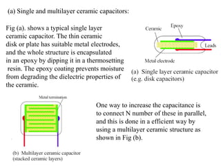
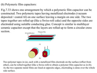
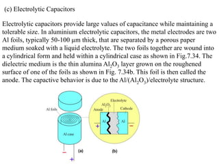
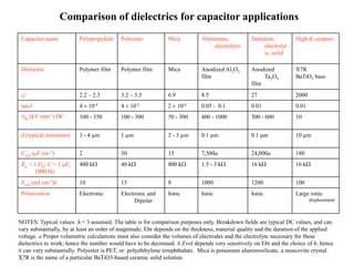
Downloaded 104 times

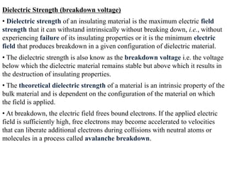
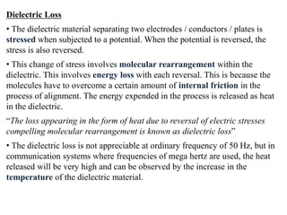
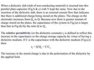
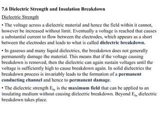
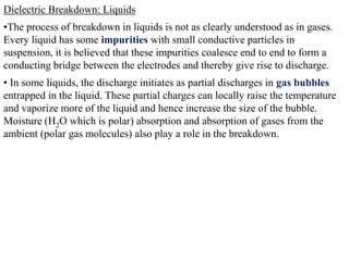
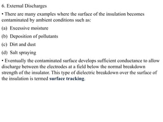
![Table: Dielectric strength (in MV/m) of various common materials:
Substance Dielectric Strength (MV/m)
Helium 0.15
Air 3.0 (depends on pressure)
Alumina 13.4
Window glass 9.8 - 13.8
Silicone oil, Mineral oil 10 - 15
Benzene 16
Polystyrene 19.7
Polyethylene 18.9 - 21.7
Neoprene rubber 15.7 - 27.6
Ultra pure Water 30
High Vacuum (field emission limited) ] 20 - 40 (depends on electrode shape)
Fused silica 25 - 40
Waxed paper 40 - 60
PTFE (Teflon) 60
Mica [11] 20 - 70
Thin films of SiO2 in ICs > 1000](https://image.slidesharecdn.com/module7-121121015239-phpapp02/85/dieletric-materials-9-320.jpg)
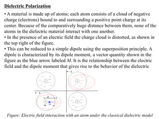
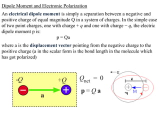
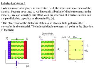
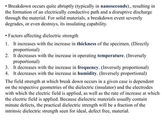
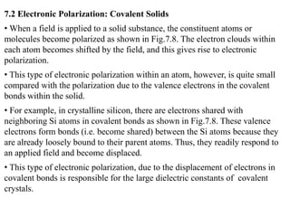
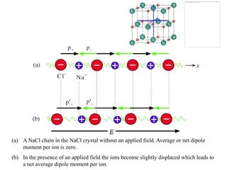
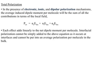
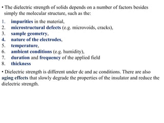
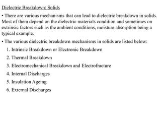
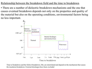
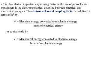
![• Consider a polarized medium alone, as shown in Fig.(b) in which every
positive charge has a negative charge next to it and vice versa. There is
therefore no net charge within the bulk. But the positive charges of the dipoles
appearing at the right hand face are not canceled by negative charges of any
dipoles at this face. There is therefore a surface charge +Qp on the right hand
face that results from the polarization of the medium.
• Similarly, there is a negative charge -Qp with the same magnitude appearing
on the left hand face due to the negative charges of the dipoles at this face.
These charges are bound and are a direct result of the polarization of the
molecules. They are termed surface polarization charges.
• Fig(c) emphasizes this aspect of dielectric behavior in an electric field by
showing the dielectric and its polarization charges only.
• We represent the polarization of a medium by a quantity called polarization
P, which is defined as the total dipole moment per unit volume,
P = 1 [p1 + p2 + ……+ pN]
Volume
Where p1, p2,….pN are the dipole moments induced at N molecules in the
volume.](https://image.slidesharecdn.com/module7-121121015239-phpapp02/85/dieletric-materials-20-320.jpg)


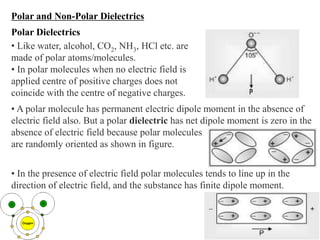
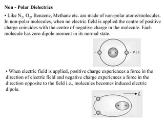
When a dielectric material is placed between the plates of a capacitor, its presence increases the capacitance compared to a vacuum. This is because the electric field causes polarization within the material by separating positive and negative charges. There are three main types of polarization in dielectric materials - electronic, ionic, and orientation. Electronic polarization occurs in all materials as the electron cloud of atoms is distorted by the electric field. Ionic polarization mainly occurs in ionic compounds as ions are displaced relative to each other. Orientation polarization involves the rotation of permanent dipoles in polar molecules to align with the electric field. The polarization ability and dielectric constant of a material depends on its atomic/molecular structure and bonding properties.