Synthesis & gate-level simulation is introduced. The key topics covered include basic concepts of logic synthesis using Design Compiler, including logic level optimization, mapping, boundary optimization, and static timing analysis. Simulation of the gate-level netlist generated after synthesis is also discussed. An example lab is outlined to synthesize a simple 8-bit microprocessor and simulate the gate-level netlist.
Define Width and Height of Core and Die (http://www.vlsisystemdesign.com/PD-F...VLSI SYSTEM Design
https://www.udemy.com/vlsi-academy
The very first step in chip design is floorplanning, in which the width and height of the chip, basically the area of the chip, is defined. A chip consists of two parts, 'core' and 'die'.
A typical design flow follows the below structure and can be broken down into multiple steps. Some of these phases happen in parallel and some in sequentially.
Requirements
A customer of a semiconductor firm is typically some other company who plans to use the chip in its systems or end products. So, the customer's requirements also play an important role in deciding how the chip should be designed.
The first step is to collect the requirements, estimate the end product's market value, and evaluate the number of resources required to do the project.
Specifications
The next step is to collect specifications that describe the functionality, interface abstractly, and over all architecture of the chip to be designed. This can be something along the lines such as:
Play
Next
Unmute
Current TimeÂ
0:00
/
DurationÂ
18:10
Â
Fullscreen
Backward Skip 10s
Play Video
Forward Skip 10s
Requires computational power to run imaging algorithms to support virtual reality.
Requires two ARM A53 processors with coherent interconnect and should run at 600 MHz.
Requires USB 3.0, Bluetooth, and PCIe 2nd gen interfaces.
It should support 1920x1080 pixel displays with an appropriate controller.
Digital Design
Because of the complex nature of modern chips, it's impossible to build something from scratch, and in many cases, many components will be reused.
For example, company A requires a FlexCAN module to interact with other modules in an automobile. They can either buy the FlexCAN design from another company to save time and effort or spend resources to build one.
It's not practical to design such a system from basic building blocks such as flip-flops and CMOS transistors.
Instead, a behavioral description is developed to analyze the design in terms of functionality, performance, and other high-level issues using a Hardware Description Language such as Verilog or VHDL.
This is usually done by a digital designer and is similar to a high-level computer programmer equipped with digital electronics skills.
Verification
Once the RTL design is ready, it needs to be verified for functional correctness.
For example, a DSP processor is expected to issue bus transactions with fetching instructions from memory and know that this will happen as expected.
The functional verification is required at this point, which is done with EDA simulators' help that can model the design and apply a different stimulus to it. This is the job of a pre-silicon verification engineer.
Logic Synthesis
Now we will convert this design into hardware schematic with real elements such as combinational gates and flip-flops. This step is called synthesis.
Logic synthesis tools enable the conversion of RTL description in HDL to a gate-level netlist. This netlist is a description of the circuit in terms of gates and connections between them.
Logic synthesis tools ensure that the netlist meets timing, area, and power specifications. Typically, they have access to different technology node
Formal equivalence checking process is a part of electronic design automation (EDA), commonly used during the development of digital integrated circuits, to formally prove that two representations of a circuit design exhibit exactly the same behavior.
Before 2000 area, delay and performance were the most important parameters, if anyone design circuit the main focus was on how much less area is occupied by the circuit on the chip and what the speed is. Now situation is changed, the performance and speed is a secondary concern. In all nanometer (deep sub-micron) technology power becomes the most important parameter in the design. Almost all portable devices run on battery power. Power consumption is a very big challenge in modern-day VLSI design as technology is going to shrinks Because of
Increasing transistors count on small chip
Higher speed of operations
Greater device leakage currents
Static Timing Analysis is a process of checking timing violation of a design by checking all possible paths under worst conditions.Any deisgn with out meeting timing requirements is undesirable.STA plays vital role in chip designing .
Visit https://www.vlsiuniverse.com/
https://www.vlsiuniverse.com/2020/05/complete-asic-design-flow.html
This is the standard VLSI design flow that every semiconductor company follows. The complete ASIC design flow is explained by considering each and every stage.
Physical verification will verify that the post-layout netlist and the layout are equivalent. i.e. all connections specified in the netlist is present in the layout. This article explains physical verification.
This is a custom GUI, which eases fixing violations either by adding buffer, cloning or sizing. Drop down menu item is created in ICC2 layout window. Desired terminals can be selected by dragging or adding points in rectilinear fashion and desired locations can be selected for adding new buffer.
Synthesis in VLSI is the process of converting your code (program) into a circuit. In terms of logic gates, synthesis is the process of translating an abstract design into a properly implemented chip. Hardware Description Languages (HDLs) are specific programming languages that are used to explain the hardware of a circuit, and the computer subsequently builds the circuit depending on the programme you provided. A “Gate Level Netlist” is what you get once you finish synthesising. This is how your circuit will appear. It demonstrates how everything is interconnected. You can alter it if you like; the computer just synthesizes this netlist based on its best judgement. The synthesizer generates better netlists as the abilities improve and they become more proficient at creating HDL programmes.
In this course, you
● Identify and apply timing arc information from a library, such as unateness, delays, and slew
● Identify cell delays from a library and calculate output slew degradation
● Use wire-load information to calculate net delays
● Identify the properties of a clock, including period, edges, and slew, and calculate the duty cycle
● Apply setup and hold checks to diagnose design violations
● Identify timing path types to calculate slack values
● Set environmental constraints, clocks constraints, and path exceptions
● Constrain a design using SDC
● Analyze reports to identify timing problems
Fusion Compiler is the next-generation RTL-to-GDSII implementation system architected to address the complexities of advanced node designs and deliver up to 20% improved PPA while reducing Time To Results (TTR) by 2X.
In VLSI design, Design for Testability (DFT) is an approach that aims to make digital circuits easier to test during the manufacturing and debugging process. DFT in VLSI design involves incorporating additional circuitry and design features such as scan chains, built-in self-test (BIST) circuits, and boundary scan cells into the chip design to facilitate testing. Design for testability in VLSI design is essential to ensure that the fabricated chips are free from any kind of manufacturing defects. It also reduces the overall test time and thereby the cost of testing, and debugging. By incorporating DFT techniques into the chip design, it becomes easier to test the structural correctness of the chip, leading to higher-quality products and faster time-to-market.
A VLSI (Very Large Scale Integration) system integrates millions of “electronic components” in a small area (few mm2 few cm2).
design “efficient” VLSI systems that has:
Circuit Speed ( high )
Power consumption ( low )
Design Area ( low )
In electronics, crosstalk is any phenomenon by which a signal transmitted on one circuit or channel of a transmission system creates an undesired effect in another circuit or channel. Crosstalk is usually caused by undesired capacitive, inductive, or conductive coupling from one circuit or channel to another.
Crosstalk is a significant issue in structured cabling, audio electronics, integrated circuit design, wireless communication and other communications systems.
Porting a Streaming Pipeline from Scala to RustEvan Chan
How we at Conviva ported a streaming data pipeline in months from Scala to Rust. What are the important human and technical factors in our port, and what did we learn?
Traditionally database systems were optimized either for OLAP either for OLTP workloads. Such mainstream DBMSes like Postgres,MySQL,... are mostly used for OLTP, while Greenplum, Vertica, Clickhouse, SparkSQL,... are oriented on analytic queries. But right now many companies do not want to have two different data stores for OLAP/OLTP and need to perform analytic queries on most recent data. I want to discuss which features should be added to Postgres to efficiently handle HTAP workload.
The increasing demand for computing power in fields such as biology, finance, machine learning is pushing the adoption of reconfigurable hardware in order to keep up with the required performance level at a sustainable power consumption. Within this context, FPGA devices represent an interesting solution as they combine the benefits of power efficiency, performance and flexibility. Nevertheless, the steep learning curve and experience needed to develop efficient FPGA-based systems represents one of the main limiting factor for a broad utilization of such devices.
In this talk, we present CAOS, a framework which helps the application designer in identifying acceleration opportunities and guides through the implementation of the final FPGA-based system. The CAOS platform targets the full stack of the application optimization process, starting from the identification of the kernel functions to accelerate, to the optimization of such kernels and to the generation of the runtime management and the configuration files needed to program the FPGA.
Taking Security Groups to Ludicrous Speed with OVS (OpenStack Summit 2015)Thomas Graf
Open vSwitch (OVS) has long been a critical component of the Neutron's reference implementation, offering reliable and flexible virtual switching for cloud environments.
Being an early adopter of the OVS technology, Neutron's reference implementation made some compromises to stay within the early, stable featureset OVS exposed. In particular, Security Groups (SG) have been so far implemented by leveraging hybrid Linux Bridging and IPTables, which come at a significant performance overhead. However, thanks to recent developments and ongoing improvements within the OVS community, we are now able to implement feature-complete security groups directly within OVS.
In this talk we will summarize the existing Security Groups implementation in Neutron and compare its performance with the Open vSwitch-only approach. We hope this analysis will form the foundation of future improvements to the Neutron Open vSwitch reference design.
Achitecture Aware Algorithms and Software for Peta and Exascaleinside-BigData.com
Jack Dongarra from the University of Tennessee presented these slides at Ken Kennedy Institute of Information Technology on Feb 13, 2014.
Listen to the podcast review of this talk: http://insidehpc.com/2014/02/13/week-hpc-jack-dongarra-talks-algorithms-exascale/
Tarantool как платформа для микросервисов / Антон Резников, Владимир Перепели...Ontico
NoSQL key-value — популярное решение, но какие преимущества и какой ценой оно даёт?
Скорость? Возможно, но ценой урезанного, по сравнению с реляционными базами данных, функционала. Но данные и приложение всё еще разделены сетевым стеком, а иногда и десятками километров оптоволокна. В крупном проекте, работающем на десятках или сотнях серверов нельзя обеспечить высокую скорость доступа к данным с каждой машины. Если хранилище достаточно быстро, то время обработки запроса окажется значительно меньше затрат на работу с сетью, а производительность приложения будут определять сетевые задержки и частота запросов к БД.
В проекте Облако@Mail.Ru мы ушли от использования чистых key-value хранилищ в пользу микросервисов на Tarantool, что позволило свести общение с хранилищем данных к минимуму.
Да, Tarantool — это еще одна NoSQL база данных, но еще это полноценный сервер приложений. Приложений, расположенных рядом с данными!
Я расскажу, как мы пришли к использованию микросервисов на основе Tarantool. Приведу несколько сценариев использования, которые работают в Облаке и могут быть легко адаптированы для другого web-проекта. Вы узнаете о компонентах, которые разработаны и опубликованы нами уже сейчас, и о дальнейших планах развития.
Regular Expressions (RE) are widely used to find patterns among data, like in genomic markers research for DNA analysis, deep packet inspection or signature-based detection for network intrusion detection system. This paper proposes a novel and efficient RE matching architecture for FPGAs, based on the concept of matching core. RE can be software-compiled into sequences of basic matching instructions that a matching core runs on input data, and can be replaced to change the RE to be matched. This architecture can easily scale up with the available resources and is customizable to multiple usage scenarios. We ran several experiments and compared the obtained results with a software solution, reaching speedups over 100x, while running at 130MHz, over a Flex-based matching application running on an Intel i7 CPU at 2.8GHz.
Fast Insights to Optimized Vectorization and Memory Using Cache-aware Rooflin...Intel® Software
Integrated into Intel® Advisor, Cache-aware Roofline Modeling (CARM) provides insight into how an application behaves by helping to determine a) how optimally it works on a given hardware, b) the main factors that limit performance, c) if the workload is memory or compute-bound, and d) the right strategy to improve application performance.
We updated the DLA system introductions here, from design, add-on functions, and applications. During the 2018~2019, we developed the tools needed for IC simulation and verification, constructed a quantize-aware & HW-aware training flow, and improved the automation of the verification. We have verified this system through FPGA and solid-state SoC.
Forklift Classes Overview by Intella PartsIntella Parts
Discover the different forklift classes and their specific applications. Learn how to choose the right forklift for your needs to ensure safety, efficiency, and compliance in your operations.
For more technical information, visit our website https://intellaparts.com
Water scarcity is the lack of fresh water resources to meet the standard water demand. There are two type of water scarcity. One is physical. The other is economic water scarcity.
Final project report on grocery store management system..pdfKamal Acharya
In today’s fast-changing business environment, it’s extremely important to be able to respond to client needs in the most effective and timely manner. If your customers wish to see your business online and have instant access to your products or services.
Online Grocery Store is an e-commerce website, which retails various grocery products. This project allows viewing various products available enables registered users to purchase desired products instantly using Paytm, UPI payment processor (Instant Pay) and also can place order by using Cash on Delivery (Pay Later) option. This project provides an easy access to Administrators and Managers to view orders placed using Pay Later and Instant Pay options.
In order to develop an e-commerce website, a number of Technologies must be studied and understood. These include multi-tiered architecture, server and client-side scripting techniques, implementation technologies, programming language (such as PHP, HTML, CSS, JavaScript) and MySQL relational databases. This is a project with the objective to develop a basic website where a consumer is provided with a shopping cart website and also to know about the technologies used to develop such a website.
This document will discuss each of the underlying technologies to create and implement an e- commerce website.
Welcome to WIPAC Monthly the magazine brought to you by the LinkedIn Group Water Industry Process Automation & Control.
In this month's edition, along with this month's industry news to celebrate the 13 years since the group was created we have articles including
A case study of the used of Advanced Process Control at the Wastewater Treatment works at Lleida in Spain
A look back on an article on smart wastewater networks in order to see how the industry has measured up in the interim around the adoption of Digital Transformation in the Water Industry.
Quality defects in TMT Bars, Possible causes and Potential Solutions.PrashantGoswami42
Maintaining high-quality standards in the production of TMT bars is crucial for ensuring structural integrity in construction. Addressing common defects through careful monitoring, standardized processes, and advanced technology can significantly improve the quality of TMT bars. Continuous training and adherence to quality control measures will also play a pivotal role in minimizing these defects.
Saudi Arabia stands as a titan in the global energy landscape, renowned for its abundant oil and gas resources. It's the largest exporter of petroleum and holds some of the world's most significant reserves. Let's delve into the top 10 oil and gas projects shaping Saudi Arabia's energy future in 2024.
Cosmetic shop management system project report.pdfKamal Acharya
Buying new cosmetic products is difficult. It can even be scary for those who have sensitive skin and are prone to skin trouble. The information needed to alleviate this problem is on the back of each product, but it's thought to interpret those ingredient lists unless you have a background in chemistry.
Instead of buying and hoping for the best, we can use data science to help us predict which products may be good fits for us. It includes various function programs to do the above mentioned tasks.
Data file handling has been effectively used in the program.
The automated cosmetic shop management system should deal with the automation of general workflow and administration process of the shop. The main processes of the system focus on customer's request where the system is able to search the most appropriate products and deliver it to the customers. It should help the employees to quickly identify the list of cosmetic product that have reached the minimum quantity and also keep a track of expired date for each cosmetic product. It should help the employees to find the rack number in which the product is placed.It is also Faster and more efficient way.
1. Synthesis &
Synthesis & Gate
Gate-
-Level
Level
Simulation
Simulation
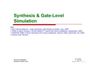
REF:
• CIC Training Manual – Logic Synthesis with Design Compiler, July, 2006
• TSMC 0.18um Process 1.8-Volt SAGE-XTM Stand Cell Library Databook, September, 2003
• TPZ973G TSMC 0.18um Standard I/O Library Databook, Version 240a, December 10, 2003
9 3G S C 0 8u Sta da d /O b a y ataboo , e s o 0a, ece be 0, 003
• Artisan User Manual
Advanced Reliable
Systems (ARES) Lab.
1
3. Outline
Basic Concept of the Synthesis
Synthesis Using Design Compiler
Synthesis Using Design Compiler
Simulation-Based Power Estimation Using PrimePower
Artisan Memory Compiler
y p
LAB
Advanced Reliable Systems (ARES) Lab. 3
4. Basic Concept of the Synthesis
Basic Concept of the Synthesis
Advanced Reliable Systems (ARES) Lab. 4
5. Cell-Based Design Flow
MATLAB/ C/ C++/ System C/
ADS/ Covergen (MaxSim)
Memory Generator
Spec.
System Level
ADS/ Covergen (MaxSim)
NC-Verilog/ ModelSim
Debussy (Verdi)/ VCS
Verilog/ VHDL Syntest
RTL Level
Design/ Power Compiler
DFT Compiler/ TetraMAX
mpiler/
Fusion
Conformal/
Formality
Logic Synthesis
Design for Test
NC-Verilog/ ModelSim
Debussy (Verdi)/ VCS
hysical
Com
gma
Blast
Gate Level
SOC Encounter/ Astro
DRC/ LVS (Calibre)
Ph
Mag
GDS II
Layout Level
Post-Layout
Verification
PVS: Calibre xRC/ NanoSim
(Time/ Power Mill)
Verification
Advanced Reliable Systems (ARES) Lab.
Tape Out
5
6. What is Synthesis
Synthesis = translation + optimization + mapping
if(high_bits == 2’b10)begin
residue = state table[i];
_ [ ];
end
else begin
residue = 16’h0000;
end Translate (HDL Compiler)
HDL Source
HDL Source
(RTL)
Optimize + Mapping
(HDL Compiler)
No Timing Info.
(HDL Compiler)
Generic Boolean
(GTECT)
Timing Info.
The synthesis is constraint driven
Advanced Reliable Systems (ARES) Lab.
Target Technology
and technology independent !!
6
7. Logic Synthesis Overview
RTL Design
HDL Design Ware
DW
Architecture
Compiler
Design Ware
Library
Developer
Optimization
Design
Compiler
Technology
Lib
Compiler
Logic
Optimization Compiler Library
p
Optimized
Optimization
Optimized
Gate-Level Netlist
Advanced Reliable Systems (ARES) Lab. 7
8. Compile
RTL code
or netlist
Optimized Design (Gate-Level Netlist)
Compile
Attributes &
Constraints
Schematic
Reports (Timing, Area, Power, …, etc)
Constraints Reports
Flatten
Technology
Lib
Structure
( g, , , , )
Logic Level Optimization
Library
(Can be set by the GUI
interface or user-defined
Script File !!)
Gate Level Optimization
Map
Technology
Library
Advanced Reliable Systems (ARES) Lab.
Library
8
9. Logic Level Optimization
Operate with Boolean representation of a circuit
Has a global effect on the overall area/speed
Has a global effect on the overall area/speed
characteristic of a design
Strategy
Strategy
Structure
Flatten (default OFF)
( )
If both are true, the design is “first flattened and then structured”
Ex:
f = acd + bcd +e
g = ae’ + be’
h = cde
f = xy + e
g = xe’
h = ye
f0 = at
f1 = d + t
f2 = t’e
f0 = ab + ac
f1 = b + c + d
f2 = b’c’e
h cde h ye
x = a + b
y = cd
(Structure)
f2 t e
t = b + c
f2 b c e
(Flatten)
Advanced Reliable Systems (ARES) Lab. 9
10. Gate Level Optimization - Mapping
Combinational Mapping
Mapping rearranges components combining and re-combining
Mapping rearranges components, combining and re-combining
logic into different components
May use different algorithms such as cloning, resizing, or
b ff i
buffering
Try to meet the design rule constraints and the timing/area goals
Sequential Mapping
Sequential Mapping
Optimize the mapping to sequential cells technology library
Analyze combinational logics surrounding a sequential cell to see
y g g q
if it can absorb the logic attribute with HDL
Try to save speed and area by using a more complex sequential
cells
cells
Advanced Reliable Systems (ARES) Lab. 10
11. Mapping
Combinational Mapping Sequential Mapping
a
a
a
b
a
b
c c
A
B D Q
AND_FF
Q
A
B
a
b
a
b
c c
a a c
c
x1 x1 x2 x4
D Q
A Q
A
B
Critical Path Critical Path
D Q
A
B
Loop_FF
Q
B
a f
g a
f
g
(assume g loading high)
Advanced Reliable Systems (ARES) Lab.
g
11
12. Boundary Optimization
Design Compiler can do some optimizations across boundaries
1. Removes logic driving unconnected output ports
2. Removes redundant inverters across boundaries
3. Propagates constants to reduce logic
Advanced Reliable Systems (ARES) Lab. 12
13. Static Timing Analysis
Main steps of STA
Break the design into sets of timing paths
Break the design into sets of timing paths
Calculate the delay of each path
Check all path delays to see if the given timing constraints are
met
Four types of paths
( )
Register - Register (Reg - Reg)
Primary Input - Register (PI - Reg)
Register - Primary Output (Reg - PO)
Register - Primary Output (Reg - PO)
Primary Input - Primary Output (PI - PO)
Advanced Reliable Systems (ARES) Lab. 13
14. Static Timing Analysis (Cont’)
To meet the setup time requirement:
Trequire >= Tarrival
- Setup Time
(T l k > 0 denotes
require arrival
Reg to Reg
Tarrival = Tclk1 + TDFF1(clk->Q) + TPATH
T T T
(Tslack > 0 denotes
“no timing violation”)
Trequire = Tclk2 - TDFF2(setup)
Tslack = Trequire - Tarrival
Clk_source
clk1
clk1
TDFF1 + Tpath
Tarrival
D Q
DFF1
D Q
DFF2
PATH
Tarrival
data
clk2
Trequire
Tsetup
Tslack
Q
clk1 Q
clk2
Advanced Reliable Systems (ARES) Lab. 14
15. Static Timing Analysis (Cont’)
PI to Reg
Tarrival = TPI(delay) + TPATH
T T T
- Setup Time
Trequire = Tclk1 - TDFF1(setup)
Tslack = Trequire - Tarrival
Clk_source
Tarrival
Tpath
D Q
DFF1
PATH
TPI(delay)
T
PI data
clk1
Trequire
Tslack
D Q
Q
clk1
Tsetup
Tarrival
Advanced Reliable Systems (ARES) Lab. 15
16. Static Timing Analysis (Cont’)
Reg to PO
Tarrival = Tclk1 + TDFF1(clk->Q) + TPATH
T T T
- Setup Time
Trequire = Tcycle - TPO(output delay)
Tslack = Trequire - Tarrival
Clk_source
clk1
clk1
TDFF1 + Tpath
T
D Q
DFF1
PATH
T
PO data
Tarrival
Trequire Tslack
D Q
Q
clk1
TPO(output delay)
Tarrival
Advanced Reliable Systems (ARES) Lab.
Tslack
16
17. Static Timing Analysis (Cont’)
PI to PO
Tarrival = TPI(delay) + TPATH
T = T - T
- Setup Time
Trequire = Tcycle - TPO(output delay)
Tslack = Trequire - Tarrival
Clk_source
TPI + Tpath
Tarrival
PATH
T
PO
PI data
Trequire Tslack
TPO(output delay)
Tarrival
Advanced Reliable Systems (ARES) Lab.
Tslack
17
18. Static Timing Analysis (Cont’)
To meet the hold time requirement:
Trequire <= Tarrival
- Hold Time
require arrival
Reg to Reg
Tarrival = Tclk1 + TDFF1(clk->Q) + TPATH
T T + T
Trequire = Tclk2 + TDFF2(hold)
Tslack = Tarrival - Trequire
Clk source
Clk_source
clk1
TDFF1 + Tpath
clk2
D Q
DFF1
D Q
DFF2
PATH
Tarrival
data 1
data 0
clk2
T i l
Trequire
Thold
Tslack
Q
clk1 Q
clk2
Advanced Reliable Systems (ARES) Lab.
Tarrival
18
19. Static Timing Analysis (Cont’)
PI to Reg
Tarrival = TPI(delay) + TPATH
- Hold Time
Trequire = Tclk1 + TDFF(hold)
Tslack = Tarrival - Trequire
Reg to PO
g
Tarrival = Tclk1 + TDFF(clk->Q) + TPATH
Trequire = - TPO(output delay)
T l k = T i l - T i
Tslack Tarrival Trequire
PI to PO
Tarrival = TPI(delay) + TPATH
T T
Trequire = - TPO(output delay)
Tslack = Tarrival - Trequire
Advanced Reliable Systems (ARES) Lab. 19
22. Notice Before Synthesis
Your RTL design
Area
Cycle
Better
Functional verification by some high-level language
Also, the code coverage of your test benches should be verified (i.e. VN)
Coding style checking (i.e. n-Lint)
Time
Coding style checking (i.e. n Lint)
Good coding style will reduce most hazards while synthesis
Better optimization process results in better circuit performance
E d b i f h i
Easy debugging after synthesis
Constraints
The area and timing of your circuit are mainly determined by your
The area and timing of your circuit are mainly determined by your
circuit architecture and coding style
There is always a trade-off between the circuit timing and area
In fact, a super tight timing constraint may be worked while synthesis,
but failed in the Place & Route (P&R) procedure
Advanced Reliable Systems (ARES) Lab. 22
23. Synthesis Using Design Compiler
Synthesis Using Design Compiler
Advanced Reliable Systems (ARES) Lab. 23
24. <.synopsys_dc.setup> File
Create individual synopsys setup file for each folder
link_library : the library used for interpreting input description
Any cells instantiated in your HDL code
y y
Wire load or operating condition modules used during synthesis
target_library : the ASIC technology which the design is mapped
f
symbol_library : used for schematic generation
search_path : the path for unsolved reference library
synthetic path : designware library
synthetic_path : designware library
Advanced Reliable Systems (ARES) Lab. 24
25. <.synopsys_dc.setup> File (Cont’)
MEMs libraries are also included in this file
Ex:
MEM Libraries (.db file)
Note that the MEM DB files are converted from
the LIB files which are generated from the Artisan !!
(.synopsys_dc.setup File)
the LIB files which are generated from the Artisan !!
Advanced Reliable Systems (ARES) Lab. 25
26. Hard Macro
Memory block
Memory library files (synopsys model) are generated by memory
il
compiler
Translate library files (.lib) to db files (.db) for synthesis
Four corners: fast@-40C fast@0C typical and slow
Four corners: fast@ 40C, fast@0C, typical, and slow
Memory block
Advanced Reliable Systems (ARES) Lab. 26
27. Settings for Using Memory
Convert *.lib to *.db
> dc shell
any memory LIB file
> dc_shell
dc_shell-t> read_lib t13spsram512x32_slow_syn.lib
dc_shell-t> write_lib t13spsram512x32 -output
t13spsram512x32_slow_syn.db
Modify <.synopsys_dc.setup> File:
“*
user library name, which should
be the same as the library name
in the Artisan
set link_library “* slow.db t13spsram512x32_slow.db
dw_foundation.sldb”
set target library “slow db t13spsram512x32 slow db”
memory DB file add to the file
set target_library slow.db t13spsram512x32_slow.db
Before the synthesis, the memory HDL model should be
blocked in your netlist
y
Advanced Reliable Systems (ARES) Lab. 27
28. Test Pins Reservation
You can add the floating test pins to your design before synthesis
se: scan enable
si: scan input
so: scan output
scantest: control signal for memory shadow wrapper (i e memory is used)
scantest: control signal for memory shadow wrapper (i.e. memory is used)
Ex:
Normal IO Declaration
Test IO Declaration
The pins will be connected to scans after the scan chain insertion
Advanced Reliable Systems (ARES) Lab.
p
28
29. CHIP-Level Netlist
The CHIP-level netlist consists of your Core-level netlist and the
PADs
E CHIPv
CORE
CORNER2
CORNER1
Ex: CHIP.v
CORE.v
(CHIP-Level Declaration)
CORE
I_CLK
CLK
CORNER3 CORNER4
O_CSO
CSO
CORNER3 CORNER4
(CORE-Level Design)
(Input PAD) I_CLK CLK
PAD C
(Output PAD) CSO O_CSO
I PAD
(IO PAD D l ti )
Advanced Reliable Systems (ARES) Lab.
(Output PAD) (IO PAD Declaration)
29
30. How To Choose the IO PAD
You can reference the Databook of the IO PAD in CIC Design Kit
Generally, the “PDIDGZ” is used as the input PAD
Trade-off when considering
the output PAD
High driving SSN
Ex:
High driving SSN
Low driving Delay
Note that the loading of the
Note that the loading of the
CIC tester is 40pf
[REF: TPZ973G TSMC 0.18um Standard
I/O Library Databook, Version 240a,
December 10, 2003]
Advanced Reliable Systems (ARES) Lab.
December 10, 2003]
30
32. Getting Started
Prepare Files:
*.v files
*.db files (i.e. memory is used)
S h i i fil (i d ib d l )
Synthesis script file (i.e. described later)
linux %> dv
Tool Bar
Logic Hierarchy
Vi
View
Log Window
(GUI view of the Design Vision)
Command Line
Advanced Reliable Systems (ARES) Lab. 32
33. Read File Design Import
Read netlists or other design descriptions into Design Compiler
File/Read
Supported formats
Verilog: .v
VHDL: .vhd
System Verilog: .sv
EDIF
PLA (Berkeley Espresso): .pla
Synopsys internal formats:
DB (binary): db
DB (binary): .db
Enhance db file: .ddc
Equation: .eqn
State table: st
State table: .st
read_file -format verilog file name.v (“/usr/LAB_DV/syn/cpu.v”)
read file -format ddc file name.ddc
{ Command Line }
Advanced Reliable Systems (ARES) Lab.
read_file format ddc file name.ddc
33
34. PAD Parameters Extraction
Input PAD
Input delay
p y
Input driving
Output PAD
O t t d l
Output delay
Output loading
CHIPv
CORE.v
(delay, loading)
(delay, driving) (chip_const.tcl)
{ Command Line }
CHIP.v
current_design CHIP
characterize [get_cells CORE]
current_design CORE
write script -format dctcl -o chip const.tcl
Advanced Reliable Systems (ARES) Lab.
write_script format dctcl o chip_const.tcl
34
35. Uniquify
Select the most top design of the hierarchy
Hierarchy/Uniquify/Hierarchy
uniquify
{ Command Line }
(Design View) (Log Window)
Advanced Reliable Systems (ARES) Lab.
uniquify
35
36. Design Environment Setting Design
Environment
Setting Operating Environment
Setting Don’t Used Cells
Setting Don t Used Cells
Setting Input Driving Strength
Setting Output Loading
Setting Output Loading
Setting Input/Output Delay
Setting Wire Load Model
Setting Wire Load Model
Advanced Reliable Systems (ARES) Lab. 36
37. Setting Operating Condition
Attributes/Operating Environment/Operating Conditions
Setup/Hold time is evaluated
set_operating_conditions -max “slow” -max_library “slow” -min “fast”
-min library “fast”
{ Command Line }
Advanced Reliable Systems (ARES) Lab.
min_library fast
37
38. Setting Don’t Used Cells
Some standard cells are for special purposes
Buffering clock
Buffering clock
CLKBUF*
Inverting clock
CLKINV*
Creating delay (delay cell)
Tie cells
Tie cells
TIE*
DFT cells
SDF* and SEDF*
{ Command Line }
set_dont_use slow/CLKBUF*
set_dont_use typical/CLKBUF*
set_dont_use fast/CLKBUF*
{ Command Line }
Advanced Reliable Systems (ARES) Lab. 38
39. Setting Drive Strength/Input Delay for PADs
Assume that we use the input PAD “PDIDGZ”
my design
PAD C
FF
Q
D
b
Input PAD
(PDIDGZ)
(PDIDGZ)
set_drive [expr 0.288001] [all_inputs]
set input delay [expr 0.34] [all inputs]
{ Command Line }
Advanced Reliable Systems (ARES) Lab.
_ p _ y [ p ] [ _ p ]
39
40. Setting Load/Output Delay for PADs
Assume that we use the output PAD “PDO24CDG”
my design
FF
Q
D d
clk
Output PAD PAD
I
(PDO24CDG)
clk
OEN
(PDO24CDG)
{ Command Line }
set_load [expr 0.06132] [all_outputs]
set_output_delay [expr 2] [all_outputs]
Advanced Reliable Systems (ARES) Lab. 40
41. Setting Wire Load Model
Attributes/Operating Environment/Wire Load
Recommend
(Worst Case)
set_wire_load_model -name “tsmc18_wl10” -library “slow”
set wire lode mode “top”
{ Command Line }
Advanced Reliable Systems (ARES) Lab.
set_wire_lode_mode top
41
43. Sequential Circuit Specify Clock
Select the “clk” pin on the symbol
Attributes/Specify Clock
set fix hold: respect the hold time
set_fix_hold: respect the hold time
requirement of all clocked flip-flops
set_dont_touch_network: do not re-buffer
th l k t k
{ Command Line }
the clock network
set sys_clk clk1
creat_clock -name $sys_clk -period 10 $sys_clk
set_dont_touch_network $sys_clk
t fi h ld $ lk
{ Command Line }
Advanced Reliable Systems (ARES) Lab.
set_fix_hold $sys_clk
43
44. Setting Clock Skew
Different clock arrival time
Ex:
FF
clk
FF
FF
FF
experience
Small circuit: 0.3 ns
Large circuit: 0 5 ns (Ti i R t)
set_clock_uncertainty -setup 0.6 $sys_clk
set clock uncertainty -hold 0.5 $sys clk
{ Command Line }
Large circuit: 0.5 ns (Timing Report)
Advanced Reliable Systems (ARES) Lab.
set_clock_uncertainty hold 0.5 $sys_clk
44
45. Setting Clock Latency
Source latency is the propagation time from the actual clock origin to
the clock definition point in the design
This setting can be avoid if the design is without the clock generator
Ex:
Your Design
Origin of Clock
Source Latency
3ns
experience
Small circuit: 1 ns
Large circuit: 3 ns
Source Latency
set clock latency 1 [get clocks clk]
{ Command Line }
Large circuit: 3 ns
Advanced Reliable Systems (ARES) Lab.
set_clock_latency 1 [get_clocks clk]
45
46. Setting Ideal Clock
Since we usually let the clock tree synthesis (CTS)
procedure performed in the P&R (i e
procedure performed in the P&R (i.e.
set_dont_touch_network), the clock source driving
capability is poor
Thus, we can set the clock tree as an ideal network
without driving issues
Avoid the hazard in the timing evaluation
set ideal network [get clocks clk]
{ Command Line }
Advanced Reliable Systems (ARES) Lab.
set_ideal_network [get_clocks clk]
46
47. Setting Don’t Touch Macro
Modules have been synthesized/optimized
S t d t t h t id ti i th ith
Set dont_touch to avoid optimize the macro with
other modules
Synthesized
core
core
set dont touch module name
{ Command Line }
Advanced Reliable Systems (ARES) Lab. 47
set_dont_touch module_name
49. Combination Circuit – Maximum Delay
Constraints
For combinational circuits primarily (i.e. design with no clock)
Select the start & end points of the timing path
Attributes/Optimization Constraints/Timing Constraints
Attributes/Optimization Constraints/Timing Constraints
Ex:
Maximum
Maximum
Delay
Constraint
(5ns = 200 MHz)
Minimum
Delay
Delay
Constraint
Advanced Reliable Systems (ARES) Lab. 49
51. Setting Area/Fanout Constraint
Attributes/Optimization
Constraints/Design
Constraints
If you only concern the circuit
area but don’t care about the
area, but don t care about the
timing
You can set the max area
constraints to 0
constraints to 0
set_max_area 0
set max fanout 32 [get designs CORE]
{ Command Line }
Advanced Reliable Systems (ARES) Lab.
set_max_fanout 32 [get_designs CORE]
51
52. Compile the Design Compile the
Design
Design/Compile Design
compile -map_effort high -boundary_optimization
compile ultra -no autoungroup (time consuming)
{ Command Line }
Advanced Reliable Systems (ARES) Lab.
compile_ultra -no_autoungroup (time consuming)
52
53. Example for DFT Insertion DFT Insertion
####DB mode####
set_dft_configuration -autofix
set dft configuration -shadow wrapper
DB
Mode
{ Command Line }
set_dft_configuration shadow_wrapper
set_scan_configuration -style multiplexed_flip_flop
set_scan_configuration -clock_mixing no_mix
set_scan_configuration -methodology full_scan
set scan signal test scan in -port si
Mode
set_scan_signal test_scan_in port si
set_scan_signal test_scan_out -port so
set_scan_signal test_scan_enable -port se
set_dft_signal test_mode -port scantest
set test hold 0 rst
set_test_hold 0 rst
set_test_hold 1 scantest
set_test_hold 1 se
create_test_clock -period 100 -waveform [list 40 60] [find port "clk"]
set port configuration -cell RA1SHD256x8 -clock clk
set_port_configuration cell RA1SHD256x8 clock clk
set_port_configuration -cell RA1SHD256x8 -port "Q" -tristate -read {"OEN" 0} -clock clk
set_port_configuration -cell RA1SHD256x8 -port "A" -write {"WEN" 0} -clock clk
set_port_configuration -cell RA1SHD256x8 -port "D" -write {"WEN" 0} -clock clk
set wrapper element RA1SHD256x8 -type shadow
set_ appe _e e e t S 56 8 type s ado
set_wrapper_element FJU_MEM -type shadow
set_fix_multiple_port_nets -all -constants -buffer_constants [get_designs *]
insert_dft
Advanced Reliable Systems (ARES) Lab. 53
54. Example for DFT Insertion (Cont’)
####XG mode####
create_port –dir in scan_in XG
Mode
{ Command Line }
create_port –dir out scan_out
create_port –dir in scan_en
compile –scan –boundary_optimization
set scan configuration –internal clocks single –chain count 1 –clock mixing no mix
Mode
set_scan_configuration –internal_clocks single –chain_count 1 –clock_mixing no_mix
set_dft_signal –view exist –type TestClock –timing {45 55} –port {clk}
set_dft_signal –view exist –type Reset –active 1 –port reset
set_dft_signal –view spec –type ScanEnable –port scan_en –active 1
g y
set_dft_signal –view spec –type ScanDataIn –port scan_in
set_dft_signal –view spec –type ScanDataOut –port scan_out
set_scan_path chain1 –view spec –scan_data_in scan_in –scan_data_out scan_out
create_test_protocol
dft_drc
preview_dft –show scan_clocks
set false path –from [get ports scan en]
set_false_path –from [get_ports scan_en]
insert_dft
Advanced Reliable Systems (ARES) Lab. 54
55. Compile After DFT Compile After
DFT
compile -scan
check_scan
{ Command Line }
report_test -scan_path
estimate_test_coverage
The fault coverage will be shown as below:
The fault coverage will be shown as below:
Advanced Reliable Systems (ARES) Lab. 55
57. Floating Port Removing
Due to some ports in the standard cells are not used in
your design
your design
remove_unconnected_ports -blast_buses [get_cells -hierarchical *]
{ Command Line }
Advanced Reliable Systems (ARES) Lab. 57
58. Chang Naming Rule Script Naming Rule
Changing
Purpose: Let the naming-rule definitions in the gate-level netlist are
the same as in the timing file (e.g. *.sdf file)
Also, the wrong naming rules may cause problems in the LVS
{ Command Line }
set bus_inference_style {%s[%d]}
set bus_naming_style {%s[%d]}
set hdlout_internal_busses true
{ Command Line }
change_names -hierarchy -rule verilog
define_name_rules name_rule -allowed "A-Z a-z 0-9 _" -max_length 255 -type cell
define_name_rules name_rule -allowed "A-Z a-z 0-9 _[]" -max_length 255 -type net
define name rules name rule -map {{"*cell*""cell"}}
define_name_rules name_rule -map {{ cell cell }}
define_name_rules name_rule -case_insensitive
change_names -hierarchy -rules name_rule
Advanced Reliable Systems (ARES) Lab. 58
59. Save Design Save Design
Five design files:
*.spf: test protocol file for ATPG tools (i.e. TetraMax)
*.sdc: timing constraint file for P&R
*.vg: gate-level netlist for P&R
* sdf: timing file for Verilog simulation
.sdf: timing file for Verilog simulation
*.ddc: binary file (i.e. all the constraints and synthesis results are
recorded)
{ C d Li }
REPORT WORK syn tbench script
write -f ddc -o [format "%s%s" [format "%s%s" "../WORK/" $TOP_BLOCK] ".ddc"] -
no_implicit -hier
write -f verilog -o [format "%s%s" [format "%s%s" "../WORK/" $TOP_BLOCK] “_syn.v"] -
{ Command Line }
g [ [ _ ] _ y ]
no_implicit -hier
write_sdc [format "%s%s" [format "%s%s" "../WORK/" $TOP_BLOCK] ".sdc"]
write_sdf -version 2.1 -context verilog [format "%s%s" [format "%s%s" "../WORK/"
$TOP BLOCK] “ sdf“]
Advanced Reliable Systems (ARES) Lab.
$TOP_BLOCK] .sdf ]
59
61. Report Design Hierarchy
Hierarchy report shows the component used in your each block & its
hierarchy
Design/Report Design Hierarchy
Ex:
Advanced Reliable Systems (ARES) Lab. 61
62. Report Area
Design/Report Area
2
Ex: (0.18um Cell-Library: 1 gate ≈ 10 um2)
(0.13um Cell-Library: 1 gate ≈ 5 um2)
Ex:
(um2)
Advanced Reliable Systems (ARES) Lab. 62
63. Design View
List/Design View
All the block area are listed !!
Ex:
Ex:
Advanced Reliable Systems (ARES) Lab. 63
64. Report Timing
Timing/Report Timing
setup time
Critical Path
Ex:
max: setup time
min: hold time
Slack = Data Require Time – Data Arrival Time
Advanced Reliable Systems (ARES) Lab. 64
66. Timing Slack Histogram
Timing/Endpoint Slack Totally 190 paths are in the slack range between
0 to 1.78
Ex:
Resolution
Advanced Reliable Systems (ARES) Lab. 66
67. Edit Your Own Script File
For convenient, you should edit your own synthesis script file.
Whenever you want to synthesis a new design, you just only change
some parameters in this file.
Execute Script File
Setup/Execute Script
Ex:
Setup/Execute Script
Or use “source your_
script.dc” in dc shell
p _
command line
Advanced Reliable Systems (ARES) Lab. 67
68. Gate-Level Simulation
Include the Verilog model of standard cell and gate-level netlist to
your test bench Standard Cell Library
Add the following Synopsys directives to the test bench
Gate- Level Netlist
Add the following Synopsys directives to the test bench
*.sdf File Instance Name
Delay
Advanced Reliable Systems (ARES) Lab. 68