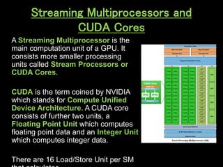
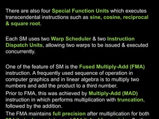
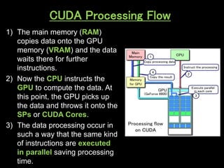
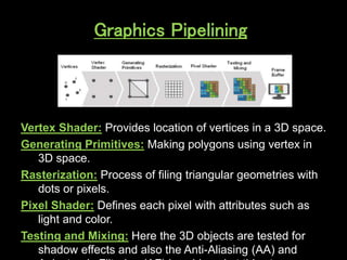
Downloaded 103 times


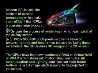
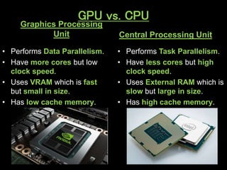


A GPU is an electronic circuit that rapidly manipulates memory to accelerate image processing and display. Modern GPUs use parallel processing, rendering each pixel and storing color, location and lighting data. GPUs have dedicated video memory and more cores than CPUs, making them better for processing large blocks of data. The Pascal GPU uses 16nm technology, HBM2 memory, NVLink interconnect and unified memory to improve performance for graphics and deep learning applications like physics simulations and image processing.