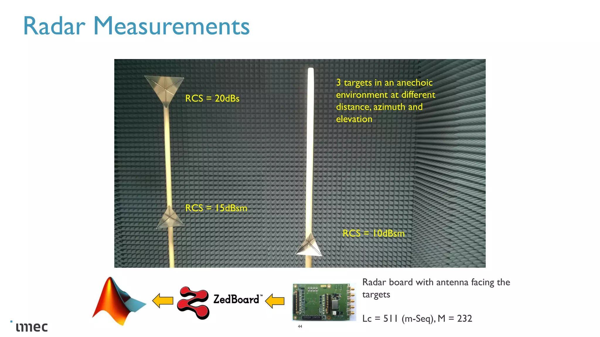
This document summarizes a public presentation about a 79GHz PMCW radar system-on-chip. Key points:
- The research investigates using nanoscale CMOS technology for 79GHz radar systems, which could enable cost-effective high-volume production and integration of large digital processing.
- A new phase-modulated continuous wave radar detection concept is introduced that is well-suited for CMOS integration.
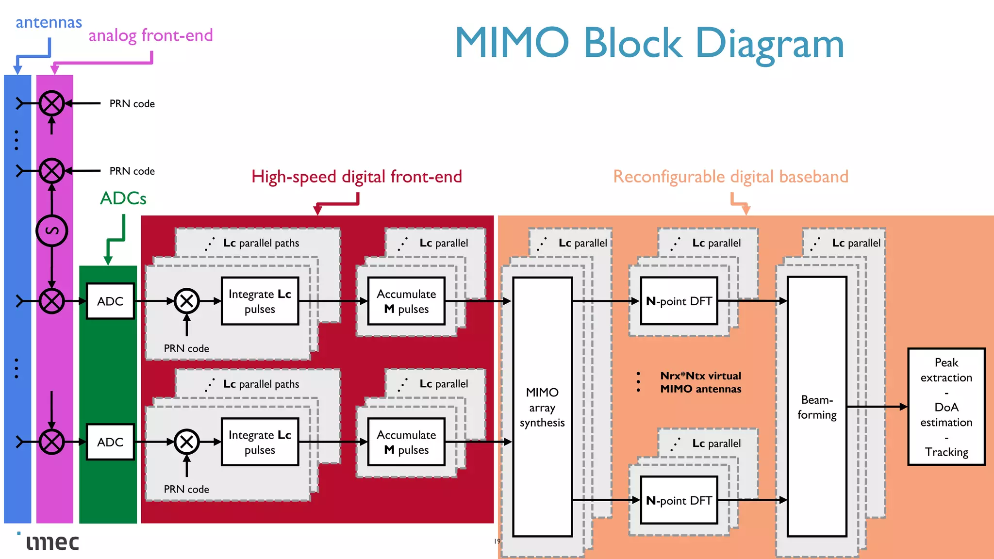
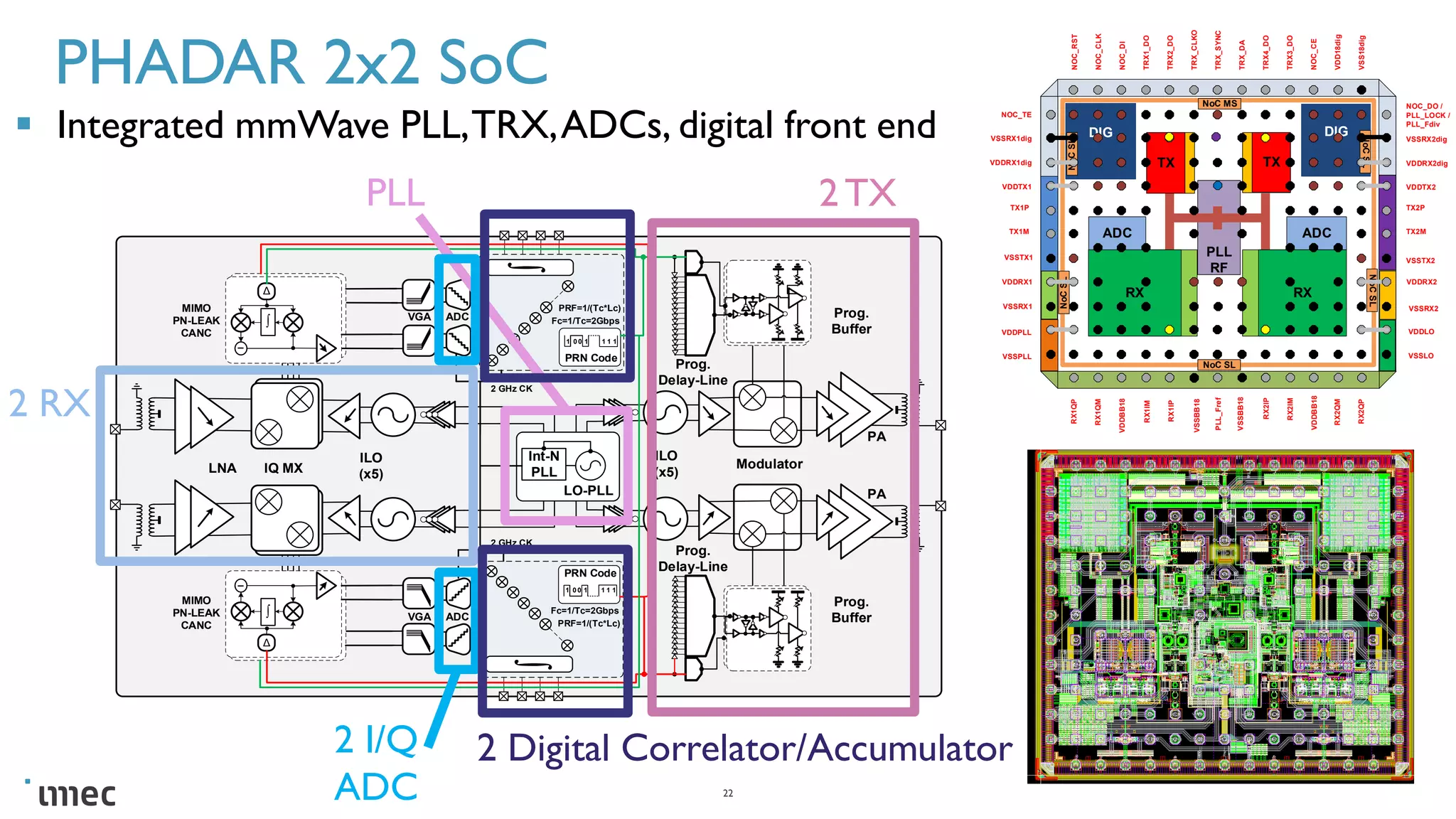
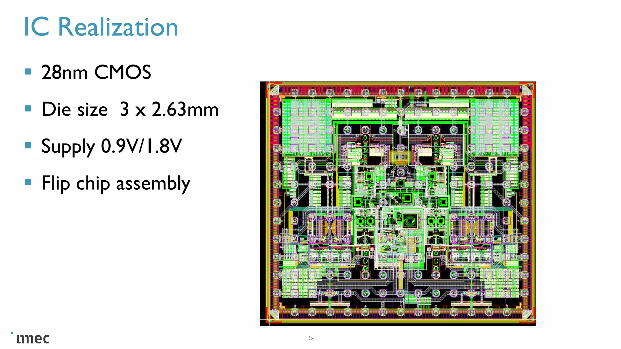
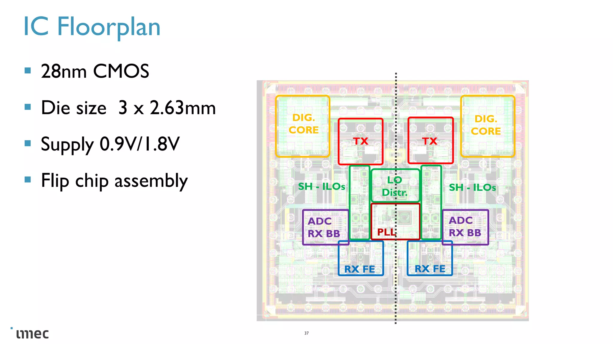
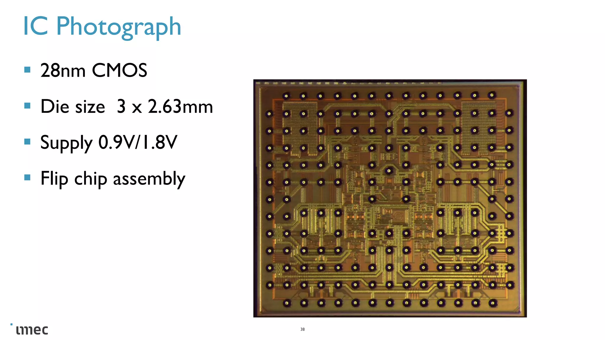
- The presented 79GHz PMCW radar SoC implements all radar functions including phased-array transceivers, ADCs, and a digital correlator on a single 3x2.63mm die using 28nm CMOS technology.


![Implementation
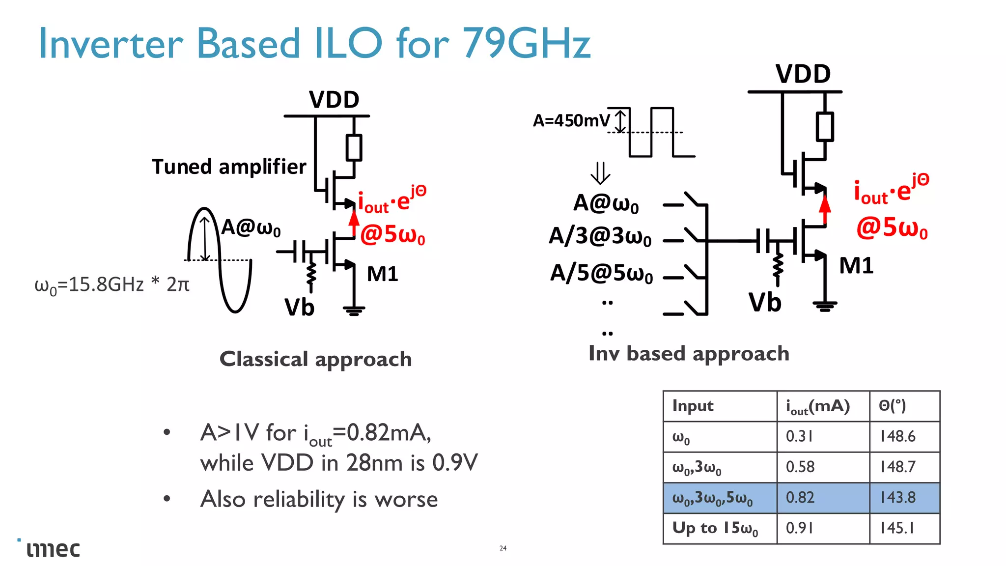
▪ Inverter chain
▪ WP/WN ratio is adjusted to have
50-50 duty cycle.
▪ Oscillator core
▪ VDC2 used to enhance self
resonance
2 2 3
20K
12um
9um
16um
13.5um
Lmos=35nm
3
VDCVDC VDC2
Vinj+
Vinj-
VCO+ VCO-
M1 M2
[3:0]
M1:M2=5:1
Qind=15 Qvar=8.5~20
Slice 25](https://image.slidesharecdn.com/acmos79ghzpmcwradarsoc-181130042259/75/A-CMOS-79GHz-PMCW-radar-SOC-25-2048.jpg)


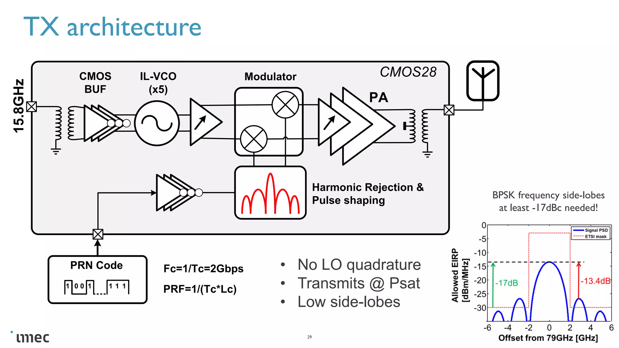


![Digital Core Block Diagram
▪ Digital core generates the sequence and performs correlation and
accumulation of the ADC samples
m’[k]
D<6:0>
(from ADC)
To TX
Out
interface
Correlator (Lc) Accumulator (M)
CK gen
CK (1.975 GHz)
Data Out
I and Q
CK CK/4
CK/<prog>
18 29
7
1
1+1
Clock Out
Data Available
TRX Sync
Other antenna path35](https://image.slidesharecdn.com/acmos79ghzpmcwradarsoc-181130042259/75/A-CMOS-79GHz-PMCW-radar-SOC-35-2048.jpg)

![A
EXTM IX ERef -17 dBm
EXT
1 GHz/Center 80 GHz Span 10 GHz
3DB
RBW 3 MHz
VBW 10 MHz
SWT 60 ms
2 AP
CLRWR
1 AP
VIEW
-110
-100
-90
-80
-70
-60
-50
-40
-30
-20
1
Marker 1 [T1 ]
-48.05 dBm
79.839743590 GHz
Date: 15.DEC.2015 15:19:49
Transmitter Measurements
▪ Pout > 10dBm
▪ 4 GHz BW
4 GHz BW
BPSK
SideLobe Supp
Measured with SAGE E band WR12 horn antenna, R&S FS-Z90 and FSU
40](https://image.slidesharecdn.com/acmos79ghzpmcwradarsoc-181130042259/75/A-CMOS-79GHz-PMCW-radar-SOC-40-2048.jpg)


![Multiband Transceivers - [Chapter 6] Multi-mode and Multi-band Transceivers](https://cdn.slidesharecdn.com/ss_thumbnails/ch6-150613070935-lva1-app6891-thumbnail.jpg?width=640&height=640&fit=bounds)


