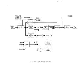
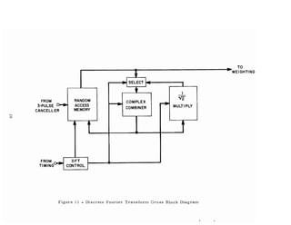
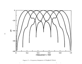
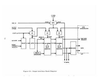
This document describes an improved radar signal processor for airport surveillance radars (ASR). It features spectral processing using a 3-pulse canceller combined with an 8-point discrete Fourier transform and adaptive thresholds. This provides a 20 dB increase in detection performance over existing ASR systems. The processor digitizes radar video signals, performs moving target indication processing, and outputs digital target reports to an air traffic control computer. It is designed to work with existing ASR systems to enhance detection of targets moving at low velocities or within ground clutter.


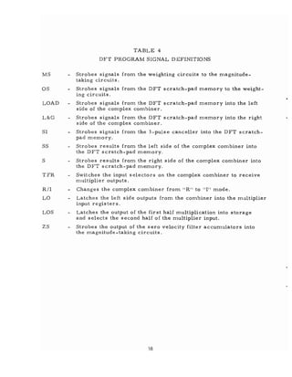
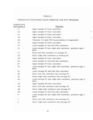
![4 9 14 19 1 7 13 19 5 16 8 19 6 4 2 19
3 8 13 18 15 2 8 14 18 10 2 13 14 12 10 8
2 7 12 17 10 16 3 9 12 4 15 7 3 1 18 16
1 6 11 16 5 11 17 4 6 17 9 1 11 9 7 5
o @]10 15 0@]1218 o IT:D 3 14 o ~15 13
-1- -2- -3- -4-
11 1 10 19 17 5 12 19 9 6 3 19 7 11 15 19
13 3 12 2 8 15 3 10 2 18 15 12 10 14 18 3
15 5 14 4 18 6 13 1 14 11 8 5 13 17 2 6
17 7 16 6 9 16 4 11 7 4 1 17 16 1 5 9
0~18 8 o 014 2 o ~13 10 0~8 12
-5- -6- -7- -8-
16 17 18 19
12 13 14 15
8 9 10 11
456 7
00] 2 3
-9-
4 9 14 19
3 8 13 18
2 7 12 17
1 6 11 16
o@]10 15
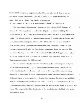
-1-
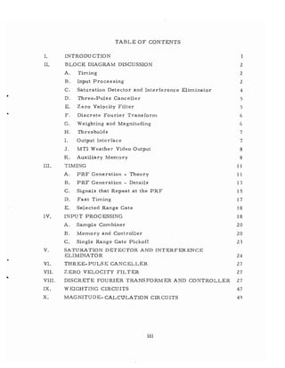
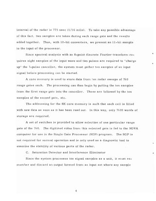
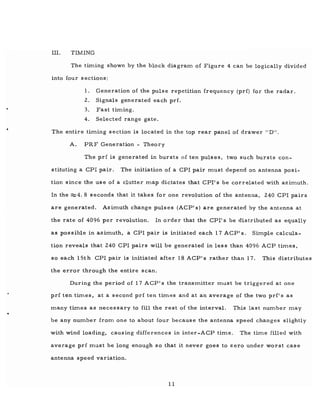
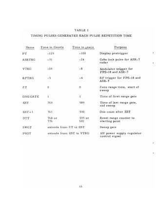
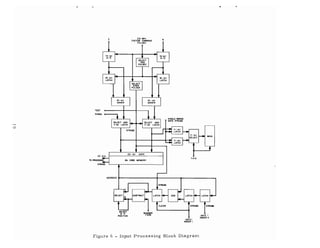
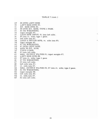
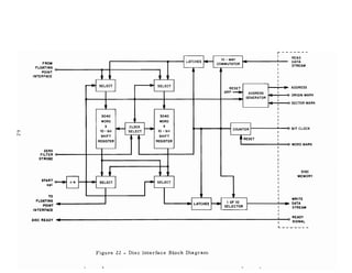
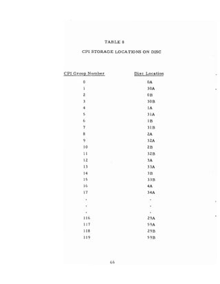
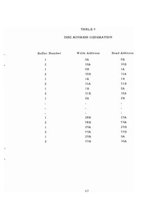
5 RANGE GATES
4 SWEEPS PER CPI
20 REQUIRED MEMORY CELLS
INCREMENT IS MODULO -19
Figure 8 - Representative Addressing - Small Array](https://image.slidesharecdn.com/drury1975atc-39ww-15318-150226001101-conversion-gate01/85/Drury-1975-atc-39_ww-15318-27-320.jpg)
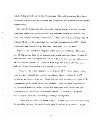
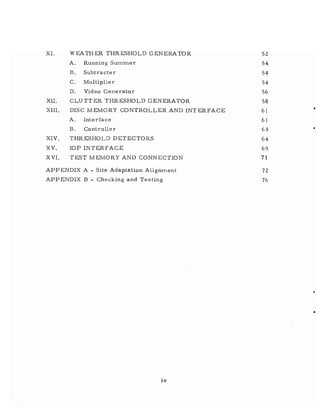
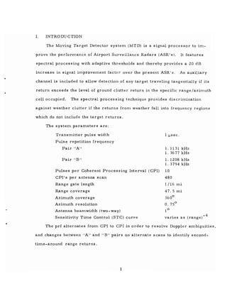
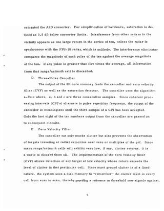
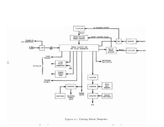
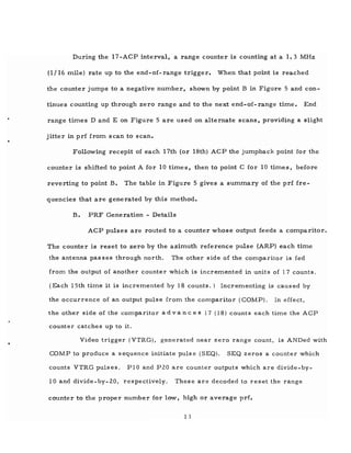
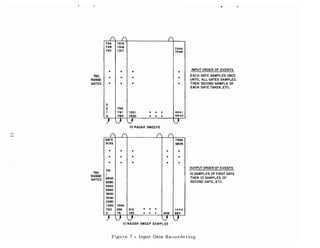
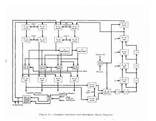
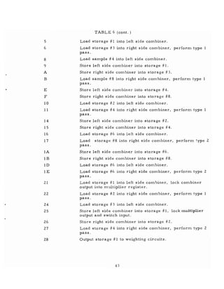
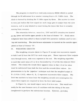
![3 pass is formed by using mode R and the multiplier, while a type 4 uses
mode I and the multiplier. Table 2 shows the complex mathematics for each
type of pass. Note that for types 3 and 4 the quantities in brackets are the sum
and difference of the parts of X2
• These are formed by putting X2
into both
sides of the combiner, placing it in the I mode and taking the result from the
left half of the combiner output as shown in Figure IZa. This complex num-
ber is then nlUltiplied by 1/ J2 and run through the combiner again in conjunc-
tion with X1 to fo rm the complete pas s.
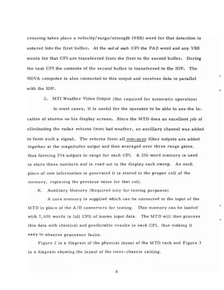
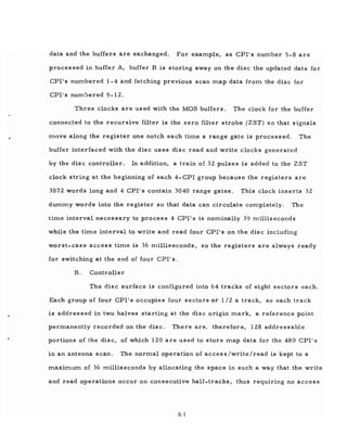
Figure 14 is a detailed block diagram of the DFT hardware. A pass
.through the combiner is performed by loading the complex number Xl from
.scratch ITlemory into a 32-bit register with strobe LOADl. Then X
2
is loaded
through selectors into a register with strobe LOAD2. This strobe also clocks
Xl along into its second input register. The two words, at this point, are pre-
sented to the various adders, negators and selectors that forITl the combiner
proper. A few hundred nsecs later the desired SUITlS and differences appear
at the output and are strobed back into meITlory. If a multiply is to take place,
the left half of the output inforITlation is clocked into a register by j2LOCK
puIs e. The ITlultiplication by IIJ2 is carried out by forming the SUITl of
(1/2 + 118 + 1/16 + 1/64 +1/256) which equals 0.707031, a reasonable approxi-
mation to the desired factor. Since there is time to spare, the real and
imaginary parts are ITlultiplied one after the other and the products stored.
The input selectors at the top of the combiner are then switched by the
jZTRANSFER signal and the new product l/Jz [R(X
2
) ±I(X
Z
)] is strobed into
32](https://image.slidesharecdn.com/drury1975atc-39ww-15318-150226001101-conversion-gate01/85/Drury-1975-atc-39_ww-15318-37-320.jpg)
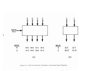
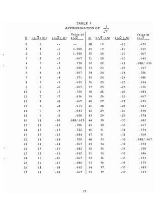
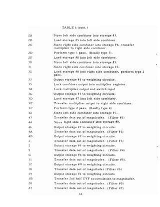
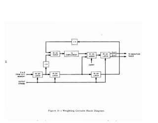
![TABLE 2
DFT PASS EQUATIONS
W has 4 values
W 1
o
W =1
W z 1/.[7: (l + j)
W
3
IIIT(-I+j)
Type 1
R(Y 1) = R(X
l
) + R(X
Z
)
I(Y
l
) = I(X
1
) + I(X
Z
)
R(Y
Z
) = R(X
l
) - R(X
Z
)
I(Y
Z
) = I(X
l
) - I(X
Z
)
Type Z
R(Y 1) = R(X
1
) - I (X
Z
)
I(Y
1
) = I(X
1
) + R(X
Z
)
R(Y
Z
) = R(X
1
) + I(X
Z
)
I(Y
Z
) = I(X
1
) - R(X
Z
)
Type 3
R(Y
1
) = R(X
1
) + IIIT[R(X
Z
) - I(X
Z
)]
I(Y
l
) = I(X
l
) + 1/;"r""[R(X
Z
) + I(X
Z
)]
R(Y
Z
) = R(X
1
) - lIlT [R(X
Z
) - I (X
Z
)]
I (YZ) I (Xl) lIlT [R (X
Z
) + I (X
Z
)]
Type 4
R(Y 1) = R(X
l
) - l/;"r"" [R(X
Z
) + I (X
Z
)]
I(Y
1
) = I(X
l
) + lIlT [R(X
Z
) - I(X
Z
)]
R(Y
Z
) = R(X
1
} + lIlT [R(X
Z
) + I(X
Z
)]
I(Y
Z
) = I(X
l
) - lIlT [R(X
Z
) - I(X
Z
)]
33](https://image.slidesharecdn.com/drury1975atc-39ww-15318-150226001101-conversion-gate01/85/Drury-1975-atc-39_ww-15318-38-320.jpg)
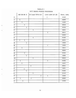
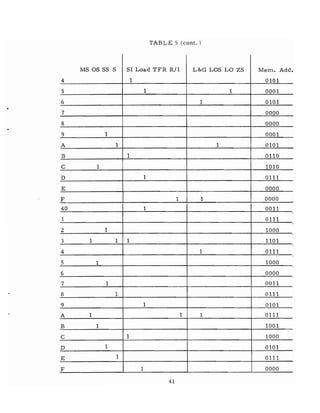
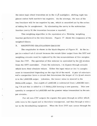
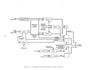

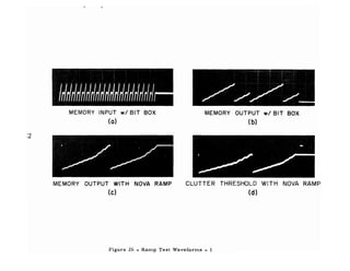
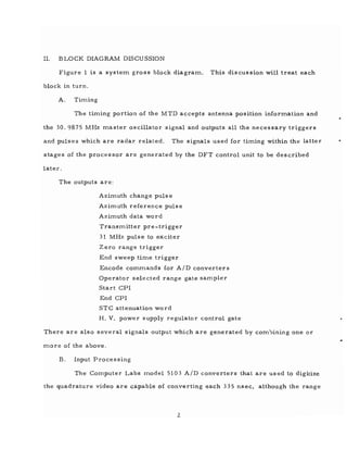
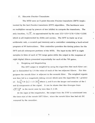
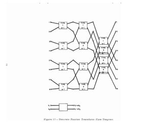
![Load program I'lumber 0025. RB and start at NOVA location 3, thus load-
ing the positive ramp into both I&Q sections of the test memory. This ramp
starts at zero level and is incremented one count in amplitude each range gate
until gate #511, then incremented two counts per gate throughout the rest of
range. The ramp therefore has a slope of 1 for the first 2/3 of range and a
slope of 2 thereafter. The signal represents DC levels in each gate with in-
creasing amplitude and with no AC components.
Each memory output (pins 15 and 13 of pos ition 14 on the upper out-
rigger) should present the waveform shown in Figure 26c. After allowing a
few minutes for the recursive filter to build up observe pin 9 of pattern 14.
The waveform is the filter output and should be like that shown in Figure 26 d.
It should be absolutely steady once the filter has stabilized. Note that Figure
26 shows two complete CP11
s in each photo and that the timing was strapped to
constant prf when the pictures were taken. If tests are made in the variable
prf mode, the first CPI will be expanded in tim,~ and the second CPI will be
compressed.
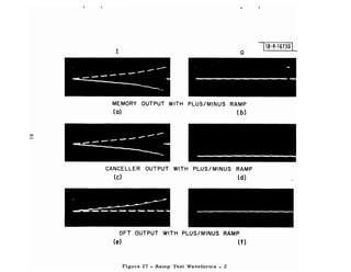
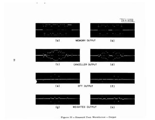
Next, the AC ramp should be loaded by restarting the NOVA at location
2. This signal is a sinewave designed to fall into filter #4 with an amplitude
that increases monotonically just as the previous ramp did. The memory out-
puts should look like Figure 27a, b. Note that t.he signal in the Q channel is al-
ways zero. Now observe the output of the three-pulse canceller by inserting
the DAC into locations 50 and 38 and probing location 14, pins 16 and 14
respectively. Tl].e waveforms should be as shown in Figure 27c, d. Next, move
the DAC to the lower outrigf!er panel positions 13 and 14 and observe pin three
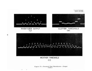
of each position. The real and imaginary parts of the discrete Fourier transform
80](https://image.slidesharecdn.com/drury1975atc-39ww-15318-150226001101-conversion-gate01/85/Drury-1975-atc-39_ww-15318-85-320.jpg)