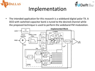
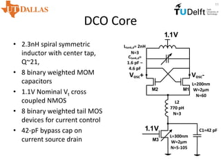
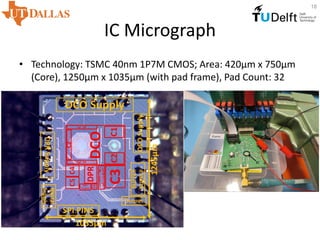
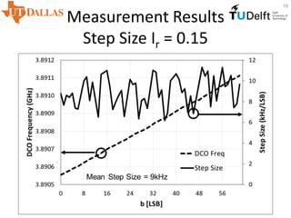
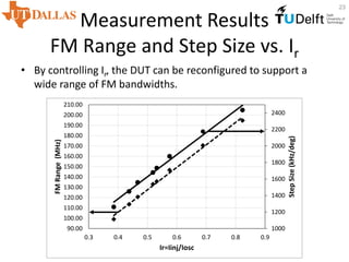
This document proposes a digitally controlled wideband frequency modulator using an injection-locked oscillator with fine frequency resolution. It achieves wideband FM modulation by controlling the phase between a delayed version of the oscillator output signal and the oscillator itself. The key advantages are scalable linear tuning range and fine frequency resolution without requiring large capacitor arrays. Simulation and measurement results show it can achieve frequency steps of 24.8 kHz and an FM range of over 2 GHz by adjusting the injection current ratio.

![Prior Art
• DCO utilizing switched capacitor array in the LC tank [1] to
modulate its’ frequency has non-linear transfer function over
a wide frequency range.
C.-M. Hung, et. al, "A digitally controlled oscillator system for SAW-less transmitters in cellular handsets,"
IEEE JSSC, vol. 41, no. 5, pp. 1160-1170, May 2006.
tanko C
C
f
f
3](https://image.slidesharecdn.com/d76c6fb2-01d3-4f56-8021-90b6497aa586-160414071905/85/Bashir_04142016-3-320.jpg)
![Prior Art
• Incrementally sized capacitor bank [3]
– Pros: Very small step size ~ 5kHz, monotonic TF
– Cons: Linear FM range 10.2 MHz, requires large number of
capacitor banks for WB modulation
J. Zhuang et al., "A 3.3 GHz LC-based digitally controlled oscillator with 5 kHz frequency resolution," in
Proc. IEEE ASSCC, 2007, pp. 428-431.
5](https://image.slidesharecdn.com/d76c6fb2-01d3-4f56-8021-90b6497aa586-160414071905/85/Bashir_04142016-5-320.jpg)
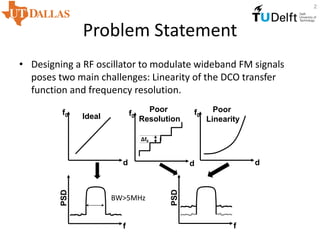
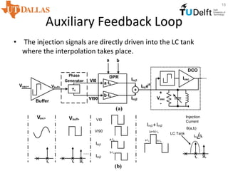
![Proposed Solution
• Oscillator is injection locked to a ‘phase delayed’ version of its’ output signal.
The output frequency ωout is given by Adler’s eqn.
• A properly calibrated time varying phase ‘θ[k]’ generates the desired FM
modulation. Within a reasonable range of θ around 0◦ generated by the Digital-
Phase Rotator (DPR), ωout increases linearly with θ.
AI
AI
kIkII
ka
kb
k
k
QI
I
k
u
u
injinjinj
o
o
osc
inj
out
31~
61~
][][
][
][
tan][
])[sin(
2
][
2
2
2
1
1
(wide-band FM)
(narrow-band FM)
LSB
ωout
Scalable linear tuning
range
τc
DPR
a b
0º
≈ 90º
τf
Iosc
+
Vosc
-
DCO
Iinj1
Iinj2
a·Iu
b·Iu
Iosc
Iinj1
Iinj2
0º-45º 45º
Iinjejθ
(Adler’s Eq.)
6
I. Bashir, R.B. Staszewski, P. T. Balsara, "A Digitally Controlled Injection-Locked Oscillator with Fine Frequency
Resolution," IEEE Journal of Solid-State Circuits, vol. 51, no. 6, pp. xxx-xxx, June 2016. (published)](https://image.slidesharecdn.com/d76c6fb2-01d3-4f56-8021-90b6497aa586-160414071905/85/Bashir_04142016-6-320.jpg)
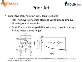
![Numerical Modeling of ILO
• Important characteristics of Injection Locked Oscillator (ILO) can be
studied through numerical modeling in MATLAB/Simulink.
(a) (b)
(c) (d)
Iinj
sgn()
R
C
L
-Iosc
X
+
Vosc
- Vosc
Itank
Iosc
Iinj
ϕ(t)
θ(t)
Iinj=Ir*Iosc
4.1 4.2 4.3 4.4 4.5 4.6 4.7 4.8
-120
-80
-40
0
40
80
120
160
Injection Frequency [GHz]
[deg]
Ir
0.5
Ir
0.8
Ir
1.0
4.1 4.2 4.3 4.4 4.5 4.6 4.7 4.8
-360
-270
-180
-90
0
90
180
270
360
[deg]
Injection Frequency [GHz]
Injection Locked
Injection Pulling
4.1 4.2 4.3 4.4 4.5 4.6 4.7 4.8
-50
-30
-10
10
30
50
[deg]
M. Heidari, A. A. Abidi, “Behavioral Models of Frequency Pulling in Oscillators,” Proc. IEEE Int. Behavioral
Modeling and Simulation Workshop (BMAS), pp. 100–104, Sept. 2007.
8](https://image.slidesharecdn.com/d76c6fb2-01d3-4f56-8021-90b6497aa586-160414071905/85/Bashir_04142016-8-320.jpg)
![Numerical Modeling of IL Oscillator
9
-180 -135 -90 -45 0 45 90 135 180
4300
4350
4400
4450
4500
4550
4600
4650
DCOFrequency[MHz]
Theta [deg]
-180 -135 -90 -45 0 45 90 135 180
0
0.2
0.4
0.6
0.8
1
NormalizedPeakVoltage
DCO Frequency
Peak Voltage
(a) (b)
Iosc
Itank
AuxiliaryLoop
sgn()
Ir· ejθ
+
Io
Ctank
tank
L
1
s
1
dt
d
х
+-
+-
Rtank
gm Differential Pair
LC Tank
Vosc
Iinj
• The conventional model is modified by adding an auxiliary
feedback loop with a controlled delay θ and the resulting transfer
function is simulated in MATLAB/Simulink.
• Desired modulation bandwidth can be achieved by adjusting Ir.
• In order to limit the loss of oscillator amplitude, -45◦ < θ < 45◦.](https://image.slidesharecdn.com/d76c6fb2-01d3-4f56-8021-90b6497aa586-160414071905/85/Bashir_04142016-9-320.jpg)
![1 2 3 4 5 6 7 8 9
0
5
10
15
20
25
Frequency [GHz]
Q
Q vs. Frequency
Qbw
Qconv
Qps
Inductor Design
• P-cell parameters:
Width=12μm, Inner
Radius = 60μm, Turns = 3,
Spacing = 2 μm
• Qbw is calculated by
resonating the inductor
with a shunt capacitor [6]
K. O, "Estimation methods for quality factors of inductors fabricated in silicon integrated circuit process technologies,"
IEEE JSSC, vol. 33, no. 8, pp. 1249-1252, Aug. 1998
12
)Re(Y
)Im(Y
atan
dω
d
2
ω
Q
11
11o
ps
)Re(Z
)Im(Z
Q
diff
diff
conv
21122211
diff
YYYY
Z
4
)()(
)(2
222113121123
1323
YYYYYY
YY
Zdiff
2-Port Inductor
Model
3-Port Inductor
Model](https://image.slidesharecdn.com/d76c6fb2-01d3-4f56-8021-90b6497aa586-160414071905/85/Bashir_04142016-12-320.jpg)
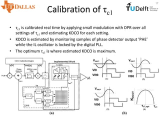
![Phase Generator (PG) Circuit
• The PG circuit
– Generates approximately quadrature signals for the DPR.
– Sets optimum phase relationship between VI0, VI90, and Vosc as shown
in Fig(b).
(c)
(b)
τc1 α1 α2 α1 + α2
Delays [deg] [deg] [deg]
1 194.6 100.5 94.1
2 129.7 35.5 94.1
3 65.8 28.4 94.2
4 2.0 92.1 94.2
V osc +
VI0
VI90
α1 α2
τc1 τc2
VI0
VI90
VI180
VI270
τc1
0: 37ps
1: 52.5ps
2: 72.7ps
3: 83.7ps
τc2
0: 55ps
1: 67ps
2: 80.5ps
3: 89.5ps
dk
IN
OUT
Vosc+
Vosc-
(a)
Vbuff+
Vbuff-
13](https://image.slidesharecdn.com/d76c6fb2-01d3-4f56-8021-90b6497aa586-160414071905/85/Bashir_04142016-13-320.jpg)
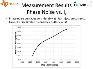
![Measurement Results
Comparison Table
[2] [5] [4] [3]
65nm 65nm 65nm 90nm
1.25 1.2 1.2
3 2.5 8 3.3
Coarse (MHz) 780 140 600
Fine (MHz) 2-12(a)
NBM WBM
0.558(a)
200(a)
60 12
9(a)
2280(a)
0.15-1.5(a)
270 5
1MHz -118 -103 -127.5 -115.1 -118
20MHz -130(c)
-130(c)
-138
26.9 16.7 16 10 2
0.27 0.27 0.32 0.18 0.18
(a) Without ΣΔ dithering.
(b) All phase noise data at DCO output.
(c) Output buffer limited.
Injection Locked
Capacitive
Tuning
Capacitive
Tuning
Injection
Locked
Capacitive
Tuning
Tuning Range (Injection Locked) (MHz)
Fine Freq Resolution (kHz)
Phase noise (dBc/Hz)(b)
Current consumption (mA)
Oscillator core area (mm2
)
Oscillator description
Frequency (GHz) 4.6
Tuning Range (Capacitive) 2100
Mode
This Work
Technology 40nm
Supply Voltage (V) 1.1
26](https://image.slidesharecdn.com/d76c6fb2-01d3-4f56-8021-90b6497aa586-160414071905/85/Bashir_04142016-26-320.jpg)
![References
• http://www.researchgate.net/profile/Imran_Bashir5
– “An SoC with Automatic Bias Calibration of an RF Oscillator ”
– “Mitigation of RF Oscillator Pulling through Adjustable Phase
Shifting”
• [1] C.-M. Hung, et. al, "A digitally controlled oscillator system for SAW-less
transmitters in cellular handsets," IEEE JSSC, vol. 41, no. 5, pp. 1160-1170,
May 2006.
• [2] L. Fanori, et. al, "Capacitive Degeneration in LC-Tank Oscillator for DCO
Fine-Frequency Tuning," IEEE JSSC, vol. 45, no. 12, pp. 2737-2745, 2010.
• [3] J. Zhuang et al., "A 3.3 GHz LC-based digitally controlled oscillator with 5
kHz frequency resolution," in Proc. IEEE ASSCC, 2007, pp. 428-431.
• [4] A. Visweswaran, et al., "Fine Frequency Tuning using Injection-Control in
a 1.2V 65nm CMOS Quadrature Oscillator," in IEEE RFIC, 2012.
• [5] K. Kodama, et. al, "A High Frequency Resolution Digitailly Controlled
Oscillator Using Single Period Switching Scheme," in ESSCC, Helsinki, 2011.
27](https://image.slidesharecdn.com/d76c6fb2-01d3-4f56-8021-90b6497aa586-160414071905/85/Bashir_04142016-27-320.jpg)


![Multiband Transceivers - [Chapter 6] Multi-mode and Multi-band Transceivers](https://cdn.slidesharecdn.com/ss_thumbnails/ch6-150613070935-lva1-app6891-thumbnail.jpg?width=640&height=640&fit=bounds)


