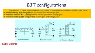
This document discusses three transistor configurations: common base, common emitter, and common collector.
- Common base has no current gain but voltage gain. Common collector has current gain but no voltage gain. Common emitter has both current and voltage gain.
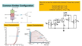
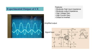
- Common emitter is the most widely used configuration. It has moderate/high input impedance, moderate output impedance, high voltage and current gain. The output is inverted.
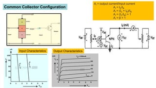
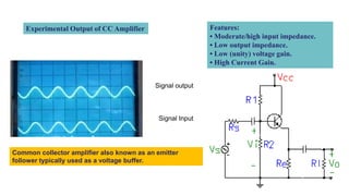
- Common collector has moderate/high input impedance, low output impedance, unity voltage gain but high current gain. It is typically used as a voltage buffer.