Downloaded 47 times

![IGBT MODEL PARAMETERS
Name Value Default Model description
TYPE_IGBT 2 2 -2:pIGBT -1:pMOSFET 1:nMOSFET 2:nIGBT
TYPE_FWD 2 2 0:no 1:static 2:dynamic including Irr
TYPE_THERM 2 0 0:isotherm 1,2:dynamic 3:dynamic_heat_pin +10:therm2
TYPE_DYN 0 12 0:stat 1:dyn +10:ext_sync +20:gate_driven
VP 4.43 5 FET Pinch-off Voltage @ref.temperature
K 85 10 FET Transfer Constant @ref.temperature
KLM 0 0 FET Channel Length Modulation Factor
A_FET 831.916882m 400m FET Saturation Factor
M_FET 1.294352379 1.2 FET Saturation Exponent
N_FET 2.3 1.7 Exponent of FET Transfer Characteristic of FET
BN 15 15 BJT Current Gain @ref.temperature
M_BJT 3.3 2 BJT Ideality Factor
ISAT_BJT 131.869869u 1n BJT Saturation Current @ref.temperature
RB_BJT 1m 0 BJT Bulk Resistance
RP_BJT 1T 1E+18 BJT Base Shunt
M_FWD 1.82 2 FWD Ideality Factor
ISAT_FWD 2u 1n FWD Saturation Current @ref.temperature
RB_FWD 1.02m 100u FWD Bulk Resistance
CIN0 165n 100n off switch input capacitance [F]
CIN1 275n 100n on switch input capacitance [F]
CR0 5.5n 5n on switch input capacitance [F]
CR1 26n 5n on switch feedback capacitance [F]
CBE 0 0 const. base emitter capacity [F]
CDS 0 0 const. drain source capacity [F]
COUT 5.6n 10n const. output capacity [F]
TAUBE 0 0 minority lifetime of IGBT base [s]
TAUFD 200n 150n minority lifetime of Diode [s]
TAUTAIL 0 100n tail current duration [s]
DETATAIL 10 10 tail current amplitude [0..100]
LC 10n 10n Collector Connector Inductance
RC 46.6032674u 100u Collector Connector Resistance
LG 0 0 Gate Connector Inductance
RG 0 200m Gate Connector Resistance
LAUX 0 0 Internal Emitter Inductance
RAUX 0 0 Internal Emitter Resistance
LE 10n 10n Emitter Connector Inductance
RE 46.6032674u 0 Emitter Connector Resistance
TEMPAMB 0 THETA Ambient Temperature
TEMPJNCTO 0 THETA Junction Temperature at Simulation Start
TNOM 25 125 Reference Temperature
VNOM 100 3k Nominal Collector-Emitter Voltage
INOM 600 3k Nominal Collector Current
SNOM_ON 30Meg 30Meg Nominal On Switch Gate Voltage Slope @VP
SNOM_OFF 30Meg 30Meg Nominal Off Switch Gate Voltage Slope @VP
VGAP 1.11 1.11 Band Gap Voltage
TC_VP 0 -200m Temperature Coefficient of VP0
TC_K 0 -140m Temperature Coefficient of K0
All Rights Reserved Copyright (C) Bee Technologies Inc. 2011](https://image.slidesharecdn.com/cm600ha-5fmodeling-110419003036-phpapp02/85/IGBT-Modeling-in-Simplorer-2-320.jpg)

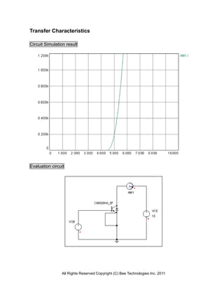


![Fall Time Characteristics
Circuit Simulation result
Evaluation circuit
IC=600A, VCC=100V
Measurement Simulation Error(%)
VGE=10V, RG=4.2Ω
Td(off) [ns] 1000 1008 0.80
Tf [ns] 500 499.7 -0.06
All Rights Reserved Copyright (C) Bee Technologies Inc. 2011](https://image.slidesharecdn.com/cm600ha-5fmodeling-110419003036-phpapp02/85/IGBT-Modeling-in-Simplorer-9-320.jpg)

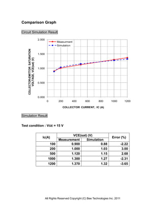
![Diode Reverse Recovery Characteristics
Circuit Simulation result
Qrr
650.00
500.00
400.00
FWD1.I [A]
300.00
200.00
FWD...
100.00
0
-100.00
-250.00
2.9000m 2.9015m 2.9025m 2.9035m 2.9050m
t
Evaluation circuit
IE=600A,
Measurement Simulation %Error
diE/dt=-1200A/us
Qrr [uC] 9.5 9.331 -1.78
All Rights Reserved Copyright (C) Bee Technologies Inc. 2011](https://image.slidesharecdn.com/cm600ha-5fmodeling-110419003036-phpapp02/85/IGBT-Modeling-in-Simplorer-12-320.jpg)

This document summarizes the key parameters of an Insulated Gate Bipolar Transistor (IGBT) device model from Mitsubishi. It includes: 1. The model parameters for the IGBT, such as voltage and current values, temperature coefficients, and capacitances. 2. Graphs comparing the simulation results using the model to measurements of the actual device's transfer and saturation characteristics. 3. The simulation circuits used to test the model and validate that it accurately represents the real IGBT's behavior.