Download to read offline
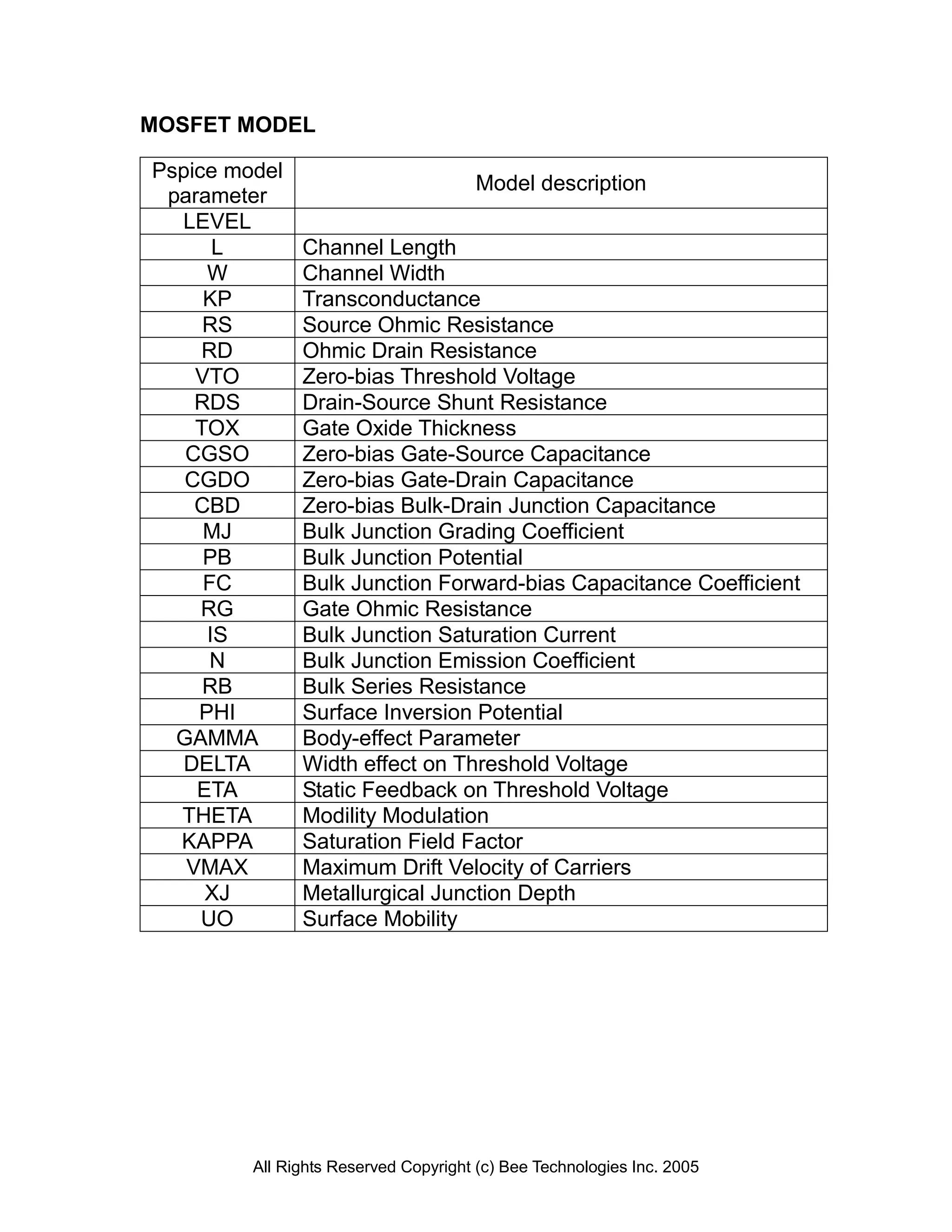
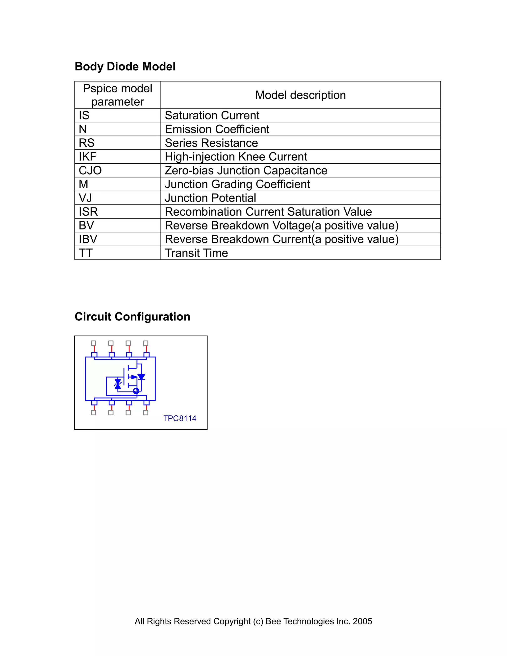
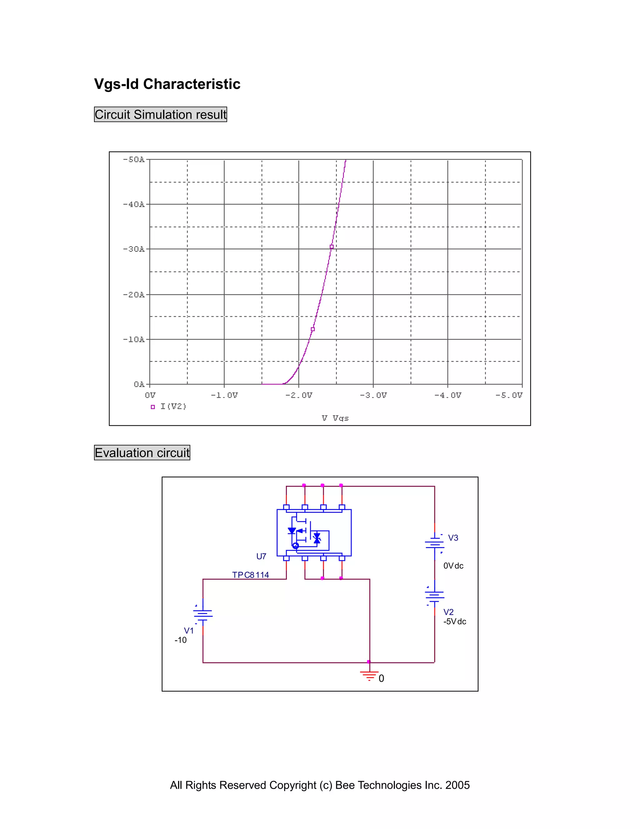
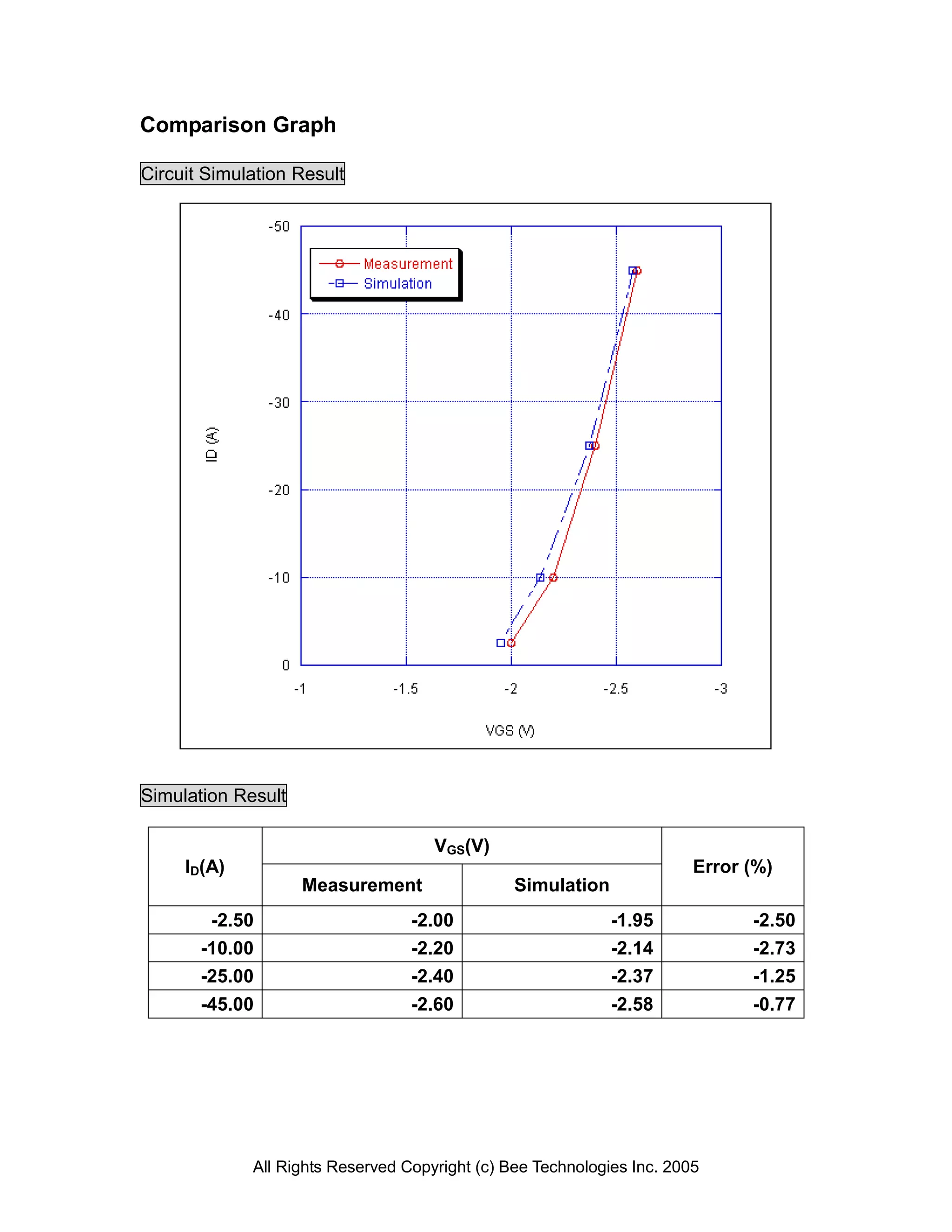
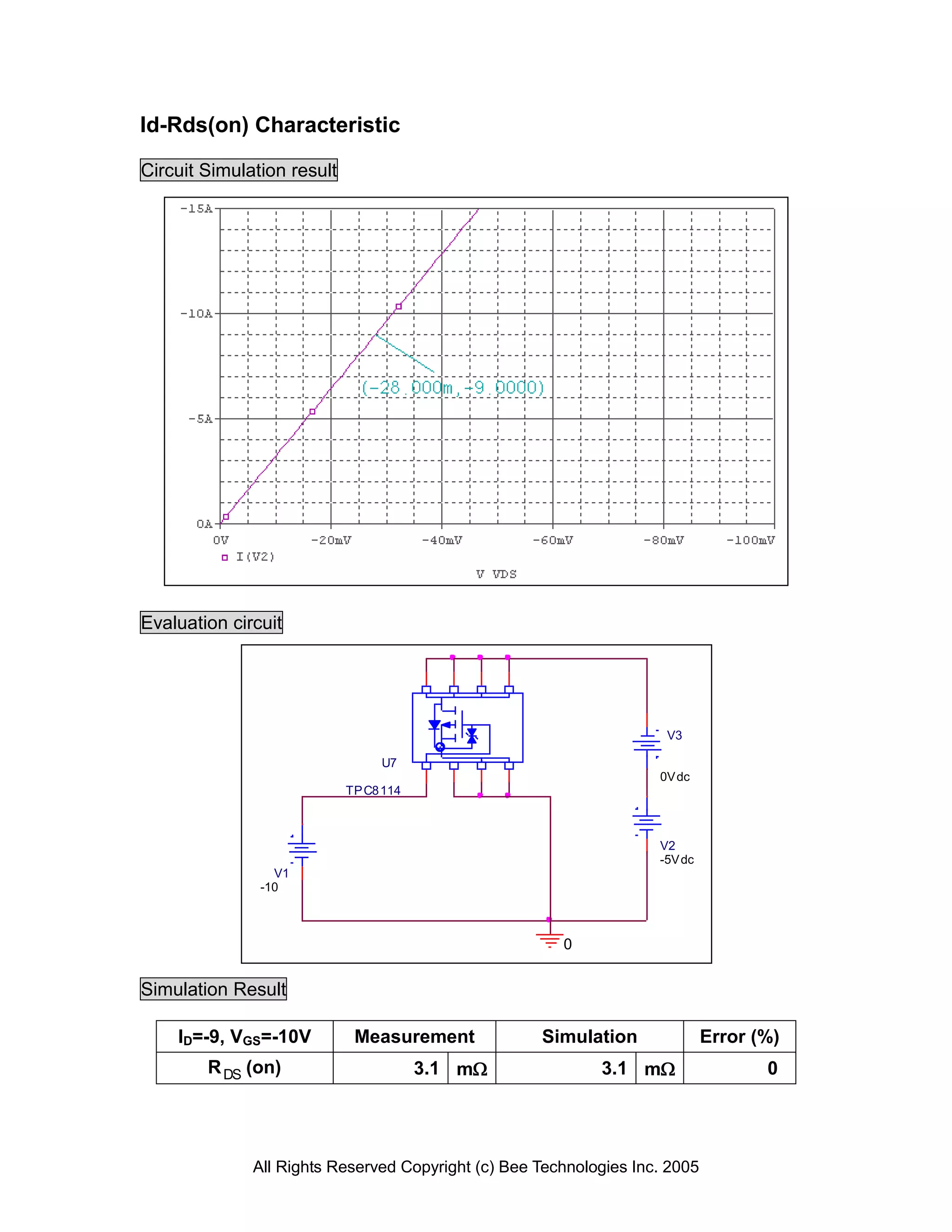
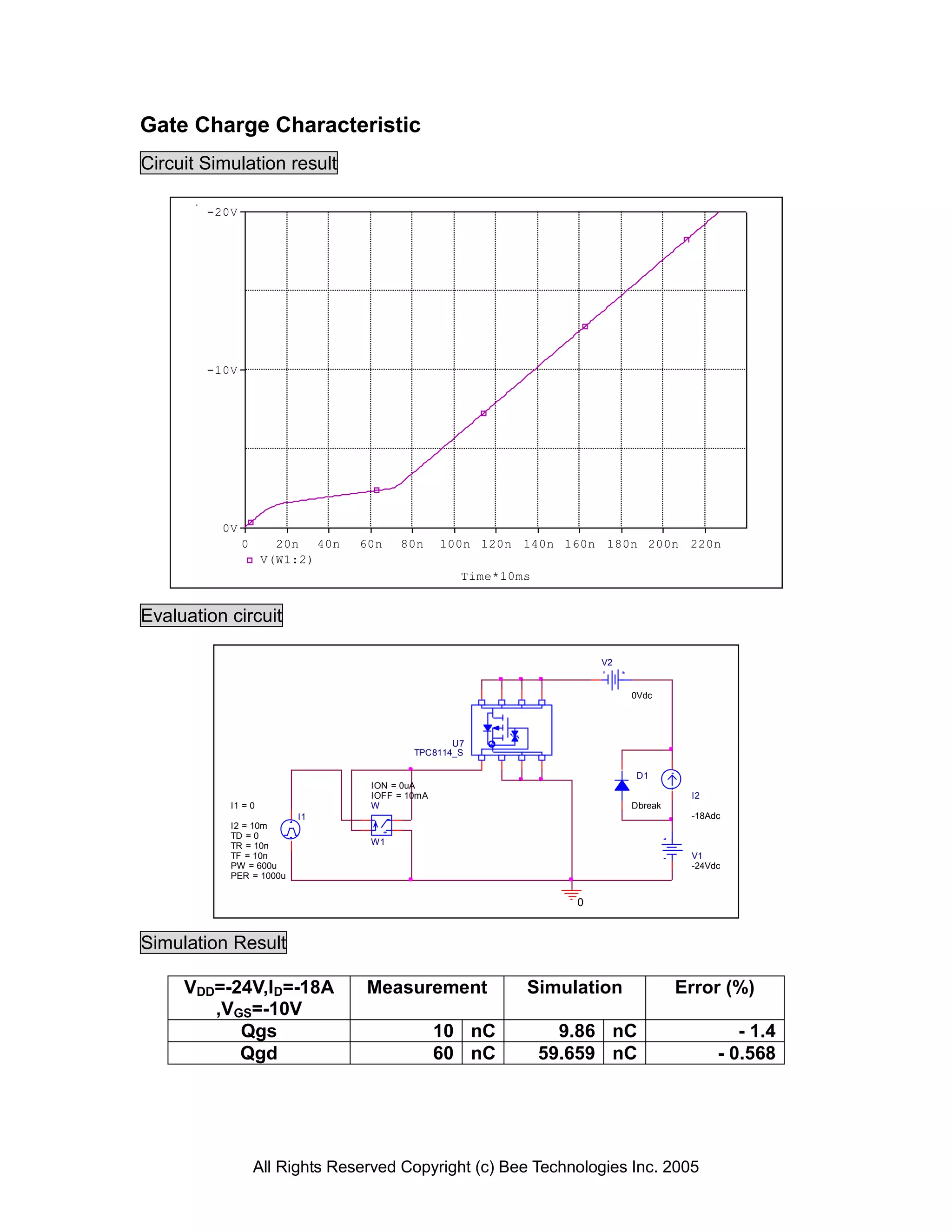
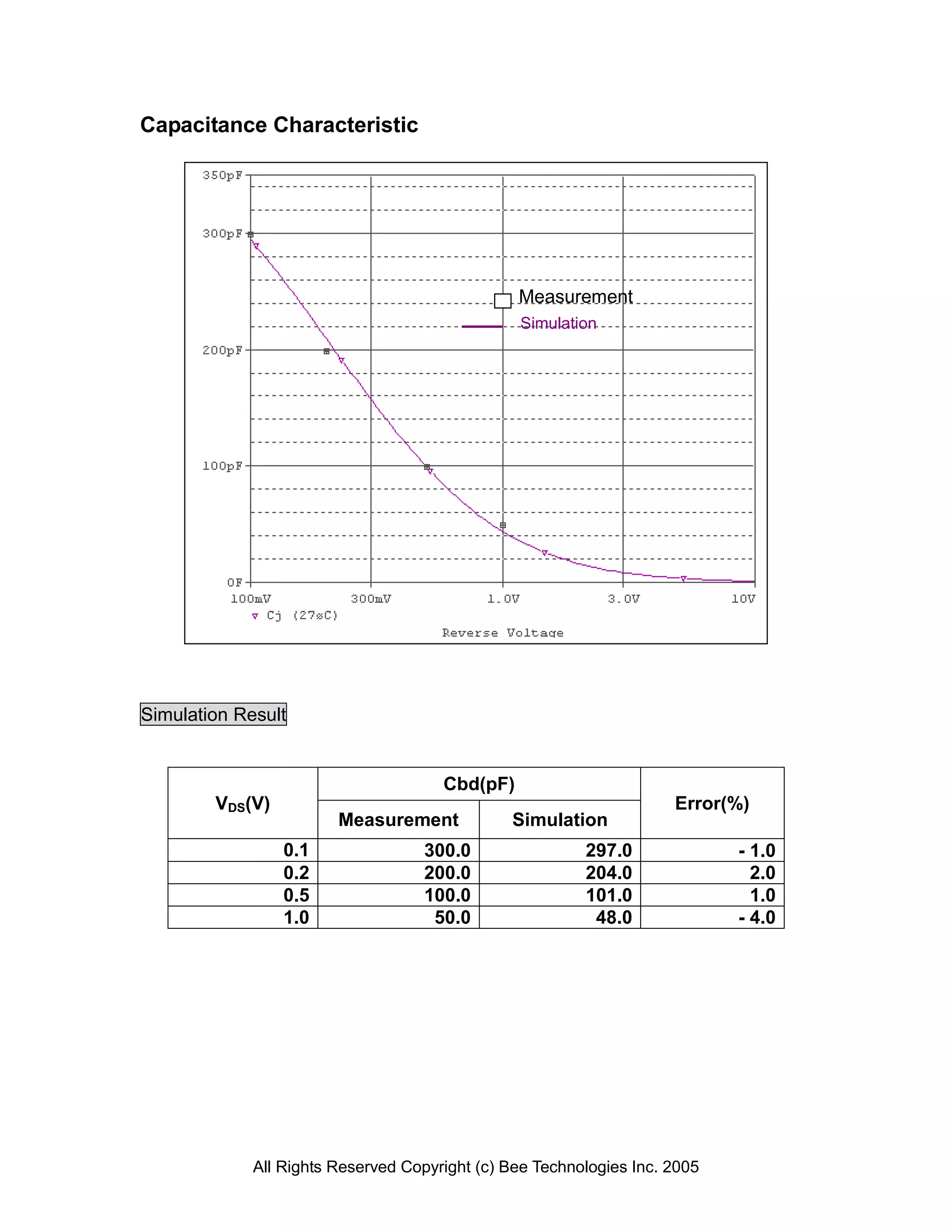
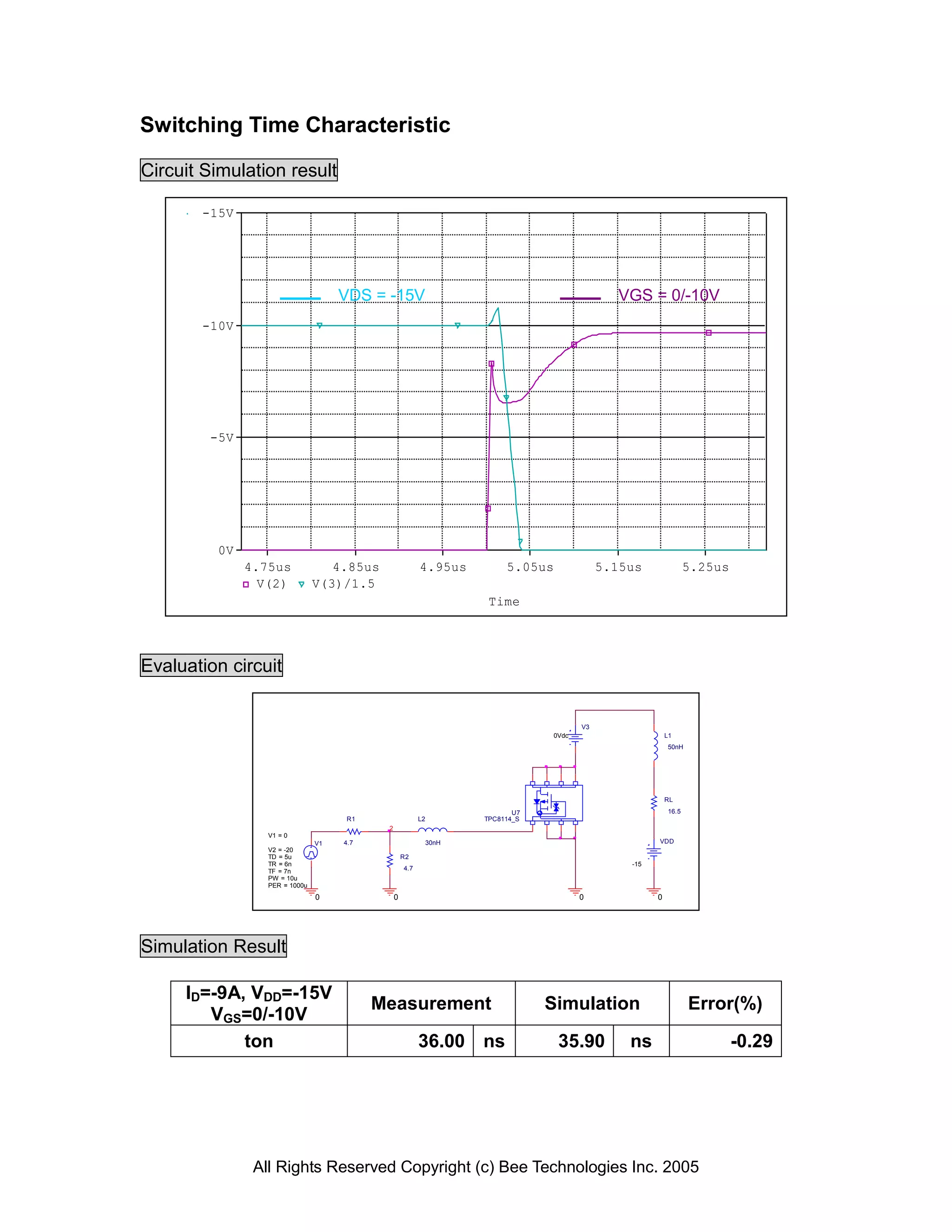
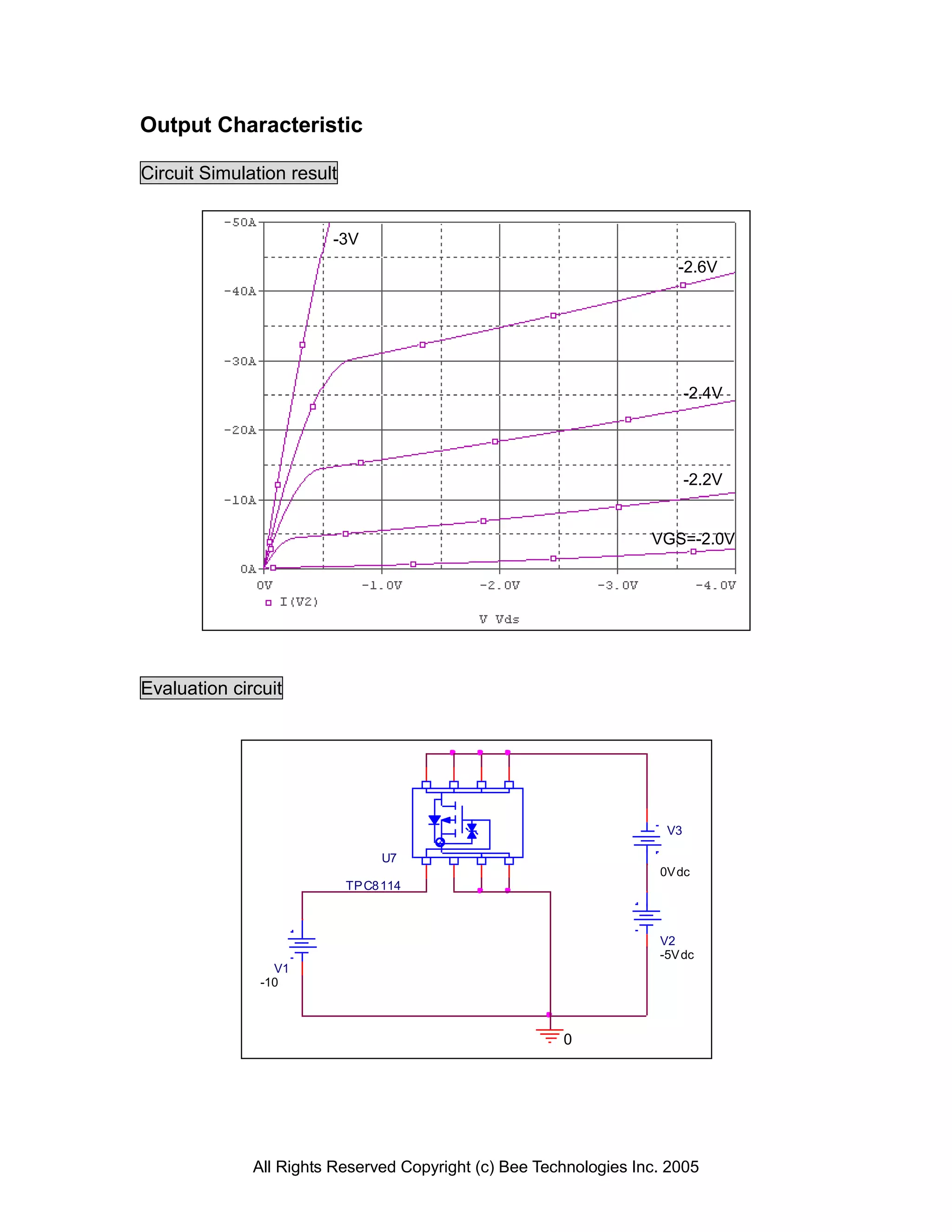
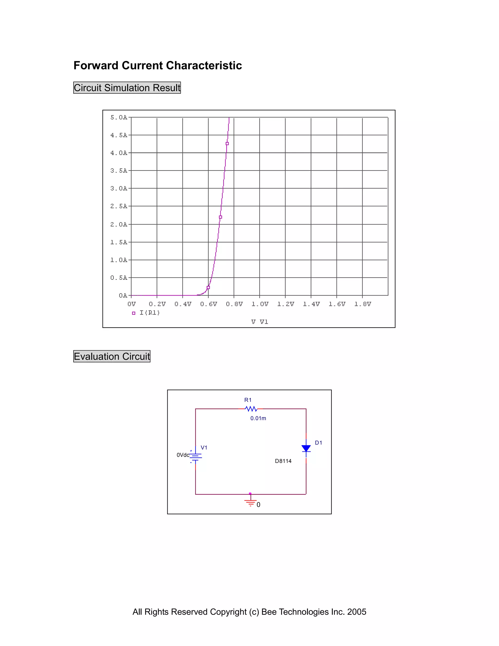
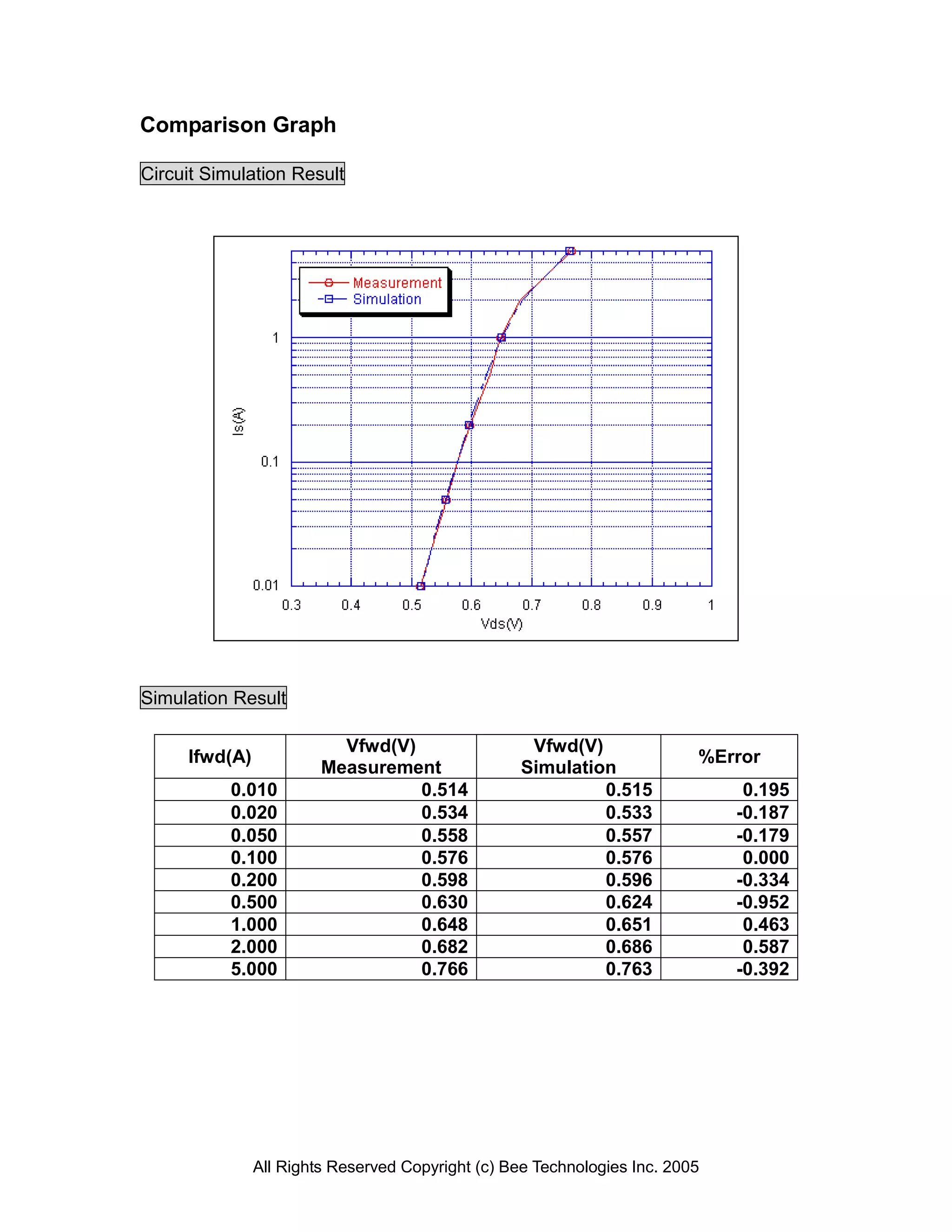
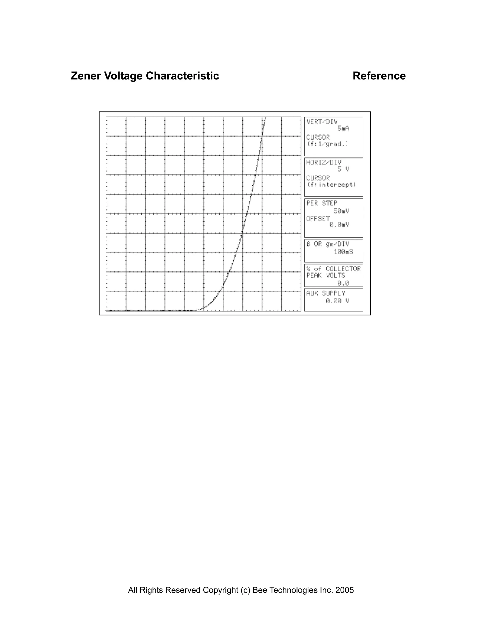

The document provides a detailed modeling report of the Toshiba power MOSFET (TPC8114) and related body diode characteristics, including various electrical parameters, PSpice models, and simulation results. It includes analyses of Vgs-Id characteristics, gate charge, capacitance, switching time, output characteristics, and reverse recovery properties, alongside measurement comparisons to highlight simulation accuracy. Additionally, it incorporates ESD protection diode analysis with zener voltage characteristics, all deemed crucial for understanding device performance.


