IC Design of Power Management Circuits (IV)Claudia Sin
by Wing-Hung Ki
Integrated Power Electronics Laboratory
ECE Dept., HKUST
Clear Water Bay, Hong Kong
www.ee.ust.hk/~eeki
International Symposium on Integrated Circuits
Singapore, Dec. 14, 2009
In semiconductor design, standard-cell methodology is a method of designing application-specific integrated circuits (ASICs) with mostly digital-logic features. Standard-cell methodology is an example of design abstraction, whereby a low-level very-large-scale integration (VLSI) layout is encapsulated into an abstract logic representation (such as a NAND gate).
Cell-based methodology – the general class to which standard cells belong – makes it possible for one designer to focus on the high-level (logical function) aspect of digital design, while another designer focuses on the implementation (physical) aspect. Along with semiconductor manufacturing advances, standard-cell methodology has helped designers scale ASICs from comparatively simple single-function ICs (of several thousand gates), to complex multi-million gate system-on-a-chip (SoC) devices.
Automated layout synthesis tool for op ampNurahmad Omar
Design Environment: Mentor Graphics
Language: Perl
OS: Unix
An algorithm is developed for designing an automatic Op-amp layout generation by using scripting language. The layout of the two-stage Op-amp will automatically draw out in the Mentor Graphics IC station by inserting the essential data. The main challenges are design a common-centroid layout template, and how to route each transistor automatically without violating the DRC (Design Rule Check).
The algorithm invokes DRC file, using circuit netlist information to generate circuit layout automatically with a common-centroid layout template.
Multiple patterning is a class of technologies for manufacturing integrated circuits (ICs), developed for photolithography to enhance the feature density. The simplest case of multiple patterning is double patterning, where a conventional lithography process is enhanced to produce double the expected number of features. The resolution of a photoresist pattern is believed to blur at around 45 nm half-pitch. For the semiconductor industry, therefore, double patterning was introduced for the 32 nm half-pitch node and below. This presentation gives us an insight of why multiple patterning is an important to give us a better resolution below 32nm.
A Novel Nonlinear Control of Boost Converter using CCM Phase PlaneIJECEIAES
Boost converter is one of fundamental DC-DC converters and used to deliver electric power with boosted voltage in many electrical systems. Several control strategies have been applied to control a boost converter delivering a constant output voltage. Generally, boost converter works in two modes; one is called a Continuous Conduction Mode (CCM). Many researches use CCM model in the controller design, but they never ensure that the controller always works in CCM. This paper proposes novel nonlinear controller of boost converter designed using the modification of flow in phase plane. The proposed controller guarantees that the boost converter works only in CCM region. The simulation result confirms that our proposed controller brings the state variables from any initial point to a desired operating point successfully.
This paper proposes the use of Embedded EZ-source
inverter system (EZSI) as a single stage power conversion
concept for adjustable speed drives (ASD) in photovoltaic
applications. Open loop and closed loop control strategy of
EZSI system are proposed. EZSI produces the same voltage
gain as Z-source inverter (ZSI) but due to the DC sources
embedded within the X- shaped impedance network, it has
the added advantage of inherent source filtering capability
and also reduced capacitor sizing. This is attained without
any extra passive filters. By controlling the shoot-through
duty ratio and modulation index, EZSI system can produce
any desired AC output voltage even greater than DC rail
voltage and it also provides ride-through capability under
voltage sag. These advantages are more significant for
adjustable speed drive (ASD) applications in order to regulate
the speed. The operational analysis, control strategy and
simulation results exemplify that an EZSI is the most
promising technique for renewable energy applications in
order to reduce the overall system complexity and thereby
improving the inverter efficiency.
Similar to Ch6 lecture slides Chenming Hu Device for IC (20)
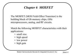
1. Modern Semiconductor Devices for Integrated Circuits (C. Hu) Slide 6-1
Chapter 6 MOSFET
The MOSFET (MOS Field-Effect Transistor) is the
building block of Gb memory chips, GHz
microprocessors, analog, and RF circuits.
Match the following MOSFET characteristics with their
applications:
• small size
• high speed
• low power
• high gain
2. Slide 6-2
6.1 Introduction to the MOSFET
Basic MOSFET structure and IV characteristics
+ +
Modern Semiconductor Devices for Integrated Circuits (C. Hu)
3. Slide 6-3
6.1 Introduction to the MOSFET
Two ways of representing a MOSFET:
Modern Semiconductor Devices for Integrated Circuits (C. Hu)
4. Slide 6-4
Early Patents on the Field-Effect Transistor
Modern Semiconductor Devices for Integrated Circuits (C. Hu)
5. Slide 6-5
Early Patents on the Field-Effect Transistor
In 1935, a British patent was issued to Oskar Heil.
A working MOSFET was not demonstrated until 1955.
Using today’s terminology, what are 1, 2, and 6?
Modern Semiconductor Devices for Integrated Circuits (C. Hu)
6. Slide 6-6
Polysilicon gate and 1.2nm SiO2
•1.2 nm SiO2 used in production. Leakage current through the
oxide limits further thickness reduction.
6.2 MOSFETs Technology
Modern Semiconductor Devices for Integrated Circuits (C. Hu)
7. Slide 6-7
6.2 Complementary MOSFETs Technology
When Vg = Vdd , the NFET is on and the PFET is off.
When Vg = 0, the PFET is on and the NFET is off.
NFET PFET
Modern Semiconductor Devices for Integrated Circuits (C. Hu)
8. Slide 6-8
CMOS (Complementary MOS) Inverter
A CMOS inverter is made of a PFET pull-up device and a
NFET pull-down device. Vout = ? if Vin = 0 V.
C:
Vin
Vdd
PFET
NFET
0V 0V
S
D
D
S
Vout
etc.)
(of interconnect,
capacitance
(a)
Modern Semiconductor Devices for Integrated Circuits (C. Hu)
9. Slide 6-9
CMOS (Complementary MOS) Inverter
• NFET and PFET can be fabricated
on the same chip.
Vin Vout
Vdd
0V
(c)
N-well
P+
N+
PFET
NFET
Contact
VddVout0V
Vin
N-well
P-substrate
(b)
P+
N+ N+ N+
P+
P+
• basic layout of a
CMOS inverter
Modern Semiconductor Devices for Integrated Circuits (C. Hu)
10. Slide 6-10
6.3 Surface Mobilities and High-Mobility FETs
LVVVWC
LVWQWQvQWI
dsnstgsoxe
dsnsinvnsinvinvds
/)(
/
m
mm
-=
==××= E
How to measure the surface mobility:
Vg = Vdd , Vgs = Vdd
Ids
Vds > 0
6.3.1 Surface Mobilities
Modern Semiconductor Devices for Integrated Circuits (C. Hu)
11. Slide 6-11
Mobility is a function of the average of the fields at the
bottom and the top of the inversion charge layer, Eb and Et .
From Gauss’s Law,
Eb = – Qdep/es
oxedepstfbt CQVV /-=
)( stfbt
s
oxe
b VV
C
E
e
--=
Therefore,
)(
)(/
/)(
stfbgs
s
oxe
tgs
s
oxe
bsinvb
sinvdept
VV
C
VV
C
EQE
QQE
e
e
e
e
--=
-=-=
-=
oxe
tgs
tgs
s
oxe
stfbtgs
s
oxe
tb
T
VV
VV
C
VVV
C
EE
6
V2.0
)V2.0(
2
)22(
2
)(
2
1
=
--=
e
e
Modern Semiconductor Devices for Integrated Circuits (C. Hu)
12. Slide 6-12
•Surface roughness
scattering is stronger
(mobility is lower) at
higher Vg, higher Vt, and
thinner Toxe.
Universal Surface Mobilities
(Vgs + Vt + 0.2)/6Toxe (MV/cm)
–(Vgs + 1.5Vt – 0.25)/6Toxe (MV/cm)
(NFET)
(PFET)
Surfacemobility(cm2/V-s)
Modern Semiconductor Devices for Integrated Circuits (C. Hu)
13. Slide 6-13
EXAMPLE: What is the surface mobility at Vgs=1 V
in an N-channel MOSFET with Vt=0.3 V and Toxe=2
nm?
Solution:
1 MV is a megavolt (106 V). From the mobility figure,
mns=190 cm2/Vs, which is several times smaller than
the bulk mobility.
MV/cm25.1
cm1012/V5.1
6/)2.0(
7
=
=
-
oxetgs TVV
Modern Semiconductor Devices for Integrated Circuits (C. Hu)
14. Slide 6-14
6.3.2 GaAs MESFET
MESFET IV characteristics are similar to MOSFET’s but does
not require a gate oxide.
Question: What is the advantage of GaAs FET over Si FET?
N-channel
N
+
metal
gate
source drain
GaAs
Semi-insulating substrate
N
+
Terms: depletion-mode transistor, enhancement-mode transistor
Modern Semiconductor Devices for Integrated Circuits (C. Hu)
15. Slide 6-15
6.3.3 HEMT, High Electron Mobility Transistor
N
+
metal gatesource drain
Undoped GaAs
N
+ ….......
N-GaAlAs
•The layer of electrons is called 2D-electron-gas, the equivalent
of the inversion or accumulation layer of a MOSFET.
•A large-Eg semiconductor serves as the “gate dielectric”.
Modern Semiconductor Devices for Integrated Circuits (C. Hu)
16. Slide 6-16
6.3.4 JFET
•The gate is a P+N junction.
•The FET is a junction field-effect transistor (JFET).
N-channel N
+
P+ gate
source drain
P-Si
N
+
Modern Semiconductor Devices for Integrated Circuits (C. Hu)
17. Slide 6-17
How to Measure the Vt of a MOSFET
6.4 Vt and Body Effect
•Method A. Vt is measured by extrapolating the Ids versus
Vgs curve to Ids = 0.
tgsdsnstgsoxedsat VVVVVC
L
W
I --= m)(
•Method B. The Vg at which Ids =0.1mA W/L
A
B
Modern Semiconductor Devices for Integrated Circuits (C. Hu)
18. Slide 6-18
maxd
s
dep
W
C
e
=
sbdeptgsoxeinv VCVVCQ --= )(
))(( sb
oxe
dep
tgsoxe V
C
C
VVC --=
• Two capacitors => two
charge components
sbtsb
oxe
dep
tsbt VVV
C
C
VVV == 00)(
• Redefine Vt as
MOSFET Vt and the Body Effect
Cdep
Coxe
Modern Semiconductor Devices for Integrated Circuits (C. Hu)
19. Slide 6-19
Body effect slows down circuits? How can it be reduced?
MOSFET Vt and the Body Effect
data
model
-2 -1 0 1 2
Vsb (V)
NFET
PFET
Vt 0
Vt0
0.6
-0.2
-0.6
0.4
-0.4
Vt (V)
0.2
• Body effect: Vt is a function
of Vsb. When the source-body
junction is reverse-biased,
Vt increases.
• Body effect coefficient:
= Cdep/Coxe
= 3Toxe / Wdep
sbtt VVV = 0
Modern Semiconductor Devices for Integrated Circuits (C. Hu)
20. Slide 6-20
Retrograde Body Doping Profiles
• Wdep does not vary with Vsb .
• Retrograde doping is popular because it reduces off-state
leakage and allows higher surface mobility.
data
model
-2 -1 0 1 2
Vsb (V)
NFET
PFET
Vt 0
Vt0
0.6
-0.2
-0.6
0.4
-0.4
Vt (V)
0.2
Wdmax for uniform doping
Wdmax for retrograde doping
Modern Semiconductor Devices for Integrated Circuits (C. Hu)
21. Slide 6-21
Uniform Body Doping
When the source/body junction is reverse-biased, there are
two quasi-Fermi levels (Efn and Efp) which are separated by
qVsb. An NMOSFET reaches threshold of inversion when Ec
is close to Efn , not Efp . This requires the band-bending to be
2B + Vsb , not 2B.
)22(
)22(
2
0
0
BsbBt
BsbB
oxe
sa
tt
VV
V
C
qN
VV
e
-
-=
is the body-effect parameter.
Modern Semiconductor Devices for Integrated Circuits (C. Hu)
22. Slide 6-22
6.5 Qinv in MOSFET
• Channel voltage
Vc=Vs at x = 0 and
Vc=Vd at x = L.
• Qinv = – Coxe(Vgs – Vcs – Vt0 – (Vsb+Vcs)
= – Coxe(Vgs – Vcs – (Vt0 + Vsb) – Vcs)
= – Coxe(Vgs – mVcs – Vt)
• m 1 + = 1 + 3Toxe/Wdmax
m is called the body-effect factor or bulk-charge factor
Modern Semiconductor Devices for Integrated Circuits (C. Hu)
23. Slide 6-23
6.6 Basic MOSFET IV Model
Ids= WQinvv= WQinvmnsE
= WCoxe(Vgs– mVcs – Vt)mnsdVcs/dx
cs
L V
tcsgsnsoxeds dVVmVVWCdxI
ds
)(
0 0 --= m
IdsL = WCoxemns(Vgs – Vt – mVds/2)Vds
dsdstgssoxeds VV
m
VVC
L
W
I )
2
( --= m
Modern Semiconductor Devices for Integrated Circuits (C. Hu)
24. Slide 6-24
Vdsat : Drain Saturation Voltage
)(0 dstgsnsoxe
ds
ds
mVVVC
L
W
dV
dI
--== m
m
VV
V tgs
dsat
-
=
Modern Semiconductor Devices for Integrated Circuits (C. Hu)
25. Slide 6-25
I = mnQinvdVcs/dx
Idsat
0 L
x
I = mnQinvdVcs/dx
Idsat
0 L
x
0 L 0 L
x x
0 L 0 L
x x
Qinv = Cox(Vg - mVcs - Vt) Qinv
(b) (f)
(c) (g)
Ec
source
drain
Ec
source
drain
- - - - - -
(d) (h)
(a) (e)Vds = Vdsat
Vds
Vdsat
Vds = Vdsat Vds > Vdsat
Vcs Vcs
Vds - Vdsat
Modern Semiconductor Devices for Integrated Circuits (C. Hu)
26. Slide 6-26
Saturation Current and Transconductance
• transconductance: gm= dIds/dVgs
2
)(
2
tgsnsoxedsat VVC
mL
W
I -= m
• linear region, saturation region
)( tgsnsoxemsat VVC
mL
W
g -= m
Modern Semiconductor Devices for Integrated Circuits (C. Hu)
30. Slide 6-30
Logic Gates
Vdd
AB
A
B
This two-input NAND
gate and many other
logic gates are
extensions of the
inverter.
Modern Semiconductor Devices for Integrated Circuits (C. Hu)
32. Slide 6-32
6.8 Velocity Saturation
sat
ns
v
E
E
E
=
1
m
• Velocity saturation has
large and deleterious
effect on the Ion of
MOSFETS
E << Esat : v = m Ens
E >> Esat : v = m Esatns
Modern Semiconductor Devices for Integrated Circuits (C. Hu)
33. Slide 6-33
6.9 MOSFET IV Model with Velocity Saturation
invds vWQI =
satdsdsdsdstgsnsoxeds EVIVV
m
VVWCLI /)
2
( ---= m
cssat
L V
dstcsgsnsoxeds dVEIVmVVWCdxI
ds
]/)([
0 0
---= m
sat
cs
csns
tcsgsoxeds
E
dx
dV
dxdV
VmVVWCI
/1
/
)(
--=
m
Modern Semiconductor Devices for Integrated Circuits (C. Hu)
36. Slide 6-36
EXAMPLE: Drain Saturation Voltage
Question: At Vgs = 1.8 V, what is the Vdsat of an NFET with
Toxe = 3 nm, Vt = 0.25 V, and Wdmax = 45 nm for (a) L =10
mm, (b) L = 1 um, (c) L = 0.1 mm, and (d) L = 0.05 mm?
Solution: From Vgs , Vt , and Toxe , mns is 200 cm2V-1s-1.
Esat= 2vsat/m ns = 8 104 V/cm
m = 1 + 3Toxe/Wdmax = 1.2
1
1
-
|
|
-
=
LEVV
m
V
sattgs
dsat
Modern Semiconductor Devices for Integrated Circuits (C. Hu)
37. Slide 6-37
(a) L = 10 mm, Vdsat= (1/1.3V + 1/80V)-1 = 1.3 V
(b) L = 1 mm, Vdsat= (1/1.3V + 1/8V)-1 = 1.1 V
(c) L = 0.1 mm, Vdsat= (1/1.3V + 1/.8V)-1 = 0.5 V
(d) L = 0.05 mm, Vdsat= (1/1.3V + 1/.4V)-1 = 0.3 V
EXAMPLE: Drain Saturation Voltage
1
-
=
LEVV
m
V
sattgs
dsat
1-
|
|
Modern Semiconductor Devices for Integrated Circuits (C. Hu)
38. Slide 6-38
Idsat with Velocity Saturation
Substituting Vdsat for Vds in Ids equation gives:
LmE
VV
Ichannel-long
LmE
VV
VV
C
mL
W
I
sat
tgs
dsat
sat
tgs
tgs
soxedsat
-
=
-
-
=
11
)(
2
2
m
Very short channel case: tgssat VVLE -<<
)( VVCWvI tgsoxesatdsat -=
• Idsat is proportional to Vgs–Vt rather than (Vgs – Vt)2 , not
as sensitive to L as 1/L.
)( LmEVVCWvI sattgsoxesatdsat --=
Modern Semiconductor Devices for Integrated Circuits (C. Hu)
39. Slide 6-39
Measured MOSFET IV
What is the main difference between the Vg dependence
of the long- and short-channel length IV curves?
0 1 2 2.5
Vds (V)
0.0
0.1
0.2
0.3
0.4
Ids(mA/mm)
L = 0.15 mm
Vgs = 2.5V
Vgs = 2.0V
Vgs = 1.5V
Vgs = 1.0V
m)
L = 2.0 mm Vgs = 2.5V
0.02
0.03
)
)
Vt = 0.7 V
Vt = 0.4 V
0 1 2 2.5
Vds (V)
0.0
0.1 Vgs = 1.0V
Vds (V)
Ids(mA/mm)
L = 2.0 mm Vgs = 2.5V
Vgs = 2.0V
Vgs = 1.5V
Vgs = 1.0V
0.0
0.01
0.02
0.03
(b)
Vt = 0.7 V
Modern Semiconductor Devices for Integrated Circuits (C. Hu)
40. Slide 6-40
PMOS and NMOS IV Characteristics
The PMOS IV is qualitatively similar to the NMOS IV,
but the current is about half as large. How can we
design a CMOS inverter so that its voltage transfer
curve is symmetric?
Modern Semiconductor Devices for Integrated Circuits (C. Hu)
41. Slide 6-41
6.9.1 Velocity Saturation vs. Pinch-Off
Instead of the pinch-off region, there is a velocity
saturation region next to the drain where Qinv is a
constant (Idsat/Wvsat).
Current saturation : the carrier velocity reaches
Vsat at the drain.
Modern Semiconductor Devices for Integrated Circuits (C. Hu)
42. Slide 6-42
6.10 Parasitic Source-Drain Resistance
• Idsat can be reduced by about 15% in a 0.1mm MOSFET.
Effect is greater in shorter MOSFETs.
• Vdsat = Vdsat0 + Idsat (Rs + Rd)
)(
1 0
0
tgs
sdsat
dsat
dsat
VV
RI
I
I
-
=• If Idsat0 Vg – Vt ,
Modern Semiconductor Devices for Integrated Circuits (C. Hu)
43. Slide 4-43
SALICIDE (Self-Aligned Silicide) Source/Drain
gate
oxide
dielectric spacercontact metal
channel
N+ source or drain
NiSi 2
or TiSi2
After the spacer is formed, a Ti or Mo film is deposited. Annealing causes
the silicide to be formed over the source, drain, and gate. Unreacted metal
(over the spacer) is removed by wet etching.
Question:
• What is the purpose of siliciding the source/drain/gate?
• What is self-aligned to what?
Modern Semiconductor Devices for Integrated Circuits (C. Hu)
44. Slide 6-44
Definitions of Channel Length
LLL g -
L, Leff ,
or Le
Lg
N N
Ldraw n
Modern Semiconductor Devices for Integrated Circuits (C. Hu)
45. Slide 6-45
6.11 Extraction of the Series Resistance and the
Effective Channel Length
L
Rds
1 2
Ldrawn (mm)
100
200
300
data
intercept
Vds
Ids
--------
Vgs - Vt = 1V
Vgs - Vt = 2V
)( tgs
drawn
dssoxe
ds VV
LL
VWC
I -
-
=
m
stgsoxe
drawn
ds
ds
ds
VVWC
LL
R
I
V
m)( -
-
=
stgsoxe
drawnds
ds
VVWC
LLI
V
m)(
)(
-
-
=
Include series resistance,
Rds Rd + Rs ,
Modern Semiconductor Devices for Integrated Circuits (C. Hu)
46. Slide 6-46
6.12 Velocity Overshoot
• Velocity saturation
should not occur in very
short MOSFETs.
• This velocity overshoot
could lift the limit on Ids .
• But…
Modern Semiconductor Devices for Integrated Circuits (C. Hu)
47. Slide 6-47
6.12 Source Velocity Limit
• Carrier velocity is limited
by the thermal velocity
with which they enter the
channel from the source.
• Idsat = WBvthxQinv
= WBvthxCoxe(Vgs – Vt)
•Similar to
)( VVCWvI tgsoxesatdsat -=
Modern Semiconductor Devices for Integrated Circuits (C. Hu)
48. Slide 6-48
6.13 Output Conductance
• Idsat does NOT saturate in the saturation region, especially
in short channel devices!
• The slope of the Ids-Vds curve in the saturation region is
called the output conductance (gds),
ds
dsat
ds
dV
dI
g
• A smaller gds is desirable for a
large voltage gain, which is
beneficial to analog and digital
circuit applications.
0 1 2 2.5
Vds (V)
0.0
0.1
0.2
0.3
0.4
Ids(mA/mm)
L = 0.15 mm
Vgs = 2.5V
Vgs = 2.0V
Vgs = 1.5V
Vgs = 1.0V
L = 2.0 mm Vgs = 2.5V
0.03
(a)
(b)
Vt = 0.4 V
Modern Semiconductor Devices for Integrated Circuits (C. Hu)
49. Slide 6-49
Example of an Amplifier
outdsintmsa
dsdsgstmsads
gg
ggi
=
=
-= Ri outds /
• The transistor operates in the saturation region. A small
signal input, vin, is applied.
• The voltage gain is gmsat/(gds + 1/R).
• A smaller gds is desirable for large voltage gain.
• Maximum available gain (or intrinsic voltage gain) is gmsat/gds
in
out
Vdd
R
NFET
in
ds
msat
out
Rg
g
-
=
)/1(
Modern Semiconductor Devices for Integrated Circuits (C. Hu)
50. Slide 6-50
6.14 High-Frequency Performance
S
G
Rin
Rd
Rs
D
Low Frequency
Model
S
G
Rin
Rd
Rs
D
Low Frequency
Model
High-frequency performance is limited
by input R and/or C.
Cutoff frequency (fT) : Frequency at
which the output current becomes equal
to the input current.
Maximum oscillation frequency (fmax)
: Frequency at which the power gain
drops to unity
iielectrodegin RRR = -
Intrinsic input resistanceGate-electrode resistance
Modern Semiconductor Devices for Integrated Circuits (C. Hu)
51. Slide 6-51
Gate-Electrode Resistance
Multi-finger layout greatly reduces
the gate electrode resistance
2
12/ fggelectrodeg NLTWR =-
ρ : resistivity of gate material,
Wf : width of each gate finger,
Tg : gate thickness,
Lg : gate length,
Nf : number of fingers.
Drain
Source
Rg-electrode
Modern Semiconductor Devices for Integrated Circuits (C. Hu)
52. Slide 6-52
Intrinsic Input Resistance
DS
Gch
Cox
Vdsat
G
Rg-electrode
Rch
ds
ds
chii
I
V
dRR ==
The gate capacitor current flows through Rch to the
source and ground.
Modern Semiconductor Devices for Integrated Circuits (C. Hu)
53. Slide 6-53
6.15 MOSFET Noises
Noise : All that corrupts the signal
External noise:
• Inductive and capacitive interferences and cross
talks created by wiring
• Needs to be controlled with shielding and circuit
layout carefully
Fundamental noise:
• Noise inherent to the electronic devices.
• Due to the random behaviors of the electric
carriers inside the device
Modern Semiconductor Devices for Integrated Circuits (C. Hu)
54. Slide 6-54
6.15.1 Thermal Noise of a Resistor
Thermal noise: caused by
random thermal motion of the
charge carriers
f
S ( f )
S : noise power density
spectrum
Modern Semiconductor Devices for Integrated Circuits (C. Hu)
55. Slide 6-55
6.15.2 MOSFET Thermal Noise
DS
Cox
Vdsat
~
v
d
2
G
dsds gfkTv /42
=
dsds fgkTi = 42
D
S D
B
G
2
dsv
2
dsi
S
2
gi
Parasitic-resistance noise
Modern Semiconductor Devices for Integrated Circuits (C. Hu)
56. Slide 6-56
6.15.3 MOSFET Flicker Noise
Many traps produce a 1/f
power density spectrum.
1/f noise
10 100 1k 10k
1E-20
1E-18
1E-16
Model representation of measurement
1/f
where = 1 + a/ = 1.15
a = 0.17A
-1
W/L = 10mm/0.28mm
Sid
(A
2
/Hz)
Frequency (Hz)
Average of 100 samples
0 250µ 500µ 750µ 1m
0
1
Trap filled half the time
ET
= EF
Vg = 0.85V
RTSWaveform
Time (s)
fkT
W
I
CfL
WKF
i AFds
ox
ds
= )(2
2
Charge trapping and releasing
by a single oxide trap generate
Random Telegraph Noise
Modern Semiconductor Devices for Integrated Circuits (C. Hu)
57. Slide 6-57
6.15.4 Signal to Noise Ratio, Noise Factor,
Noise Figure
SNR: Signal power noise power.
Noise factor: The ratio of the input SNR and output
SNR.
00 /
/
NS
NS
F ii
=
Decibel or dB:10 times the base-10 logarithm of the
noise power.
N
S
log10
Modern Semiconductor Devices for Integrated Circuits (C. Hu)
58. Slide 6-58
6.16 Memory Devices
Keep
data
without
power?
Cell size
and
cost/bit
Rewrite
cycles
Write-
one-
byte
speed
Compatible
with basic
CMOS
fabrication
Main
applications
SRAM No Large Unlimited Fastest Totally Embedded in
logic chips
DRAM No Small Unlimited Fast Needs
modification
Stand-alone
main memory
Flash
memory
(NVM)
Yes Smallest Limited Slow Needs
extensive
modification
Nonvolatile
data and code
storage
Modern Semiconductor Devices for Integrated Circuits (C. Hu)
59. Slide 6-59
6.16.1 SRAM
M1
M2
M3 M4
M5
M6
“HI”
(LOW)
“LOW”
(HI)
Vdd
BL BLC
WL
>Fastest among all
memories.
>Totally CMOS
compatible.
>Cost per bit is the
highest-- uses 6 transistors
to store one bit of data.
Modern Semiconductor Devices for Integrated Circuits (C. Hu)
60. Slide 6-60
6.16.2 DRAM
•DRAM capacitor
can only hold the data
(charge) for a limited
time because of
leakage current.
Bit-line 1
Word-line 1
Bit-line 2
Word-line 2
•Needs refresh.
•Needs ~10fF C in a
small and shrinking
area -- for refresh time
and error rate.
Modern Semiconductor Devices for Integrated Circuits (C. Hu)
61. Slide 6-61
6.16.2 DRAM capacitor technology
Capacitor
Bit-Line
Word Line
Capacitor
Bit-Line
Word Line
Stacked capacitor and
Trench capacitor
Modern Semiconductor Devices for Integrated Circuits (C. Hu)
63. Slide 6-63
Phase Change Memory
Alloy of Ge, Sb, Te has high resistivity in
amorphous phase and low resistivity in
polycrystalline phase.
Modern Semiconductor Devices for Integrated Circuits (C. Hu)
64. 3D (Multi-layer) Memory
• Epitaxy from seed windows can produce Si layers.
• Ideally memory element is simple and does not need
single-crystalline material.
Modern Semiconductor Devices for Integrated Circuits (C. Hu)
65. Resistive Memory (RRAM)
-- Organic, inorganic, metallic.. material
-- Future extension to 3-D
Modern Semiconductor Devices for Integrated Circuits (C. Hu)
66. Slide 6-66
6.17 Chapter Summary
• propagation delay
)
11
(
4 onPonN
dd
d
II
CV
• Power Consumption
offdddd IVfkCVP = 2
sbtsbt VVVV = 0)( for steep retrograde body doping
• body effect
dmaxoxe WT /3=
Modern Semiconductor Devices for Integrated Circuits (C. Hu)
67. Slide 6-67
6.17 Chapter Summary
• basic Ids model
dsdstgssoxeds VV
m
VVC
L
W
I )
2
( --= m
2.1/31 = dmaxoxe WTm
• Small and m are desirable. Therefore, small Toxe is good.
Ch.7 shows that large Wdmax is not acceptable.
• CMOS circuit speed is determined by CVdd/Idsat , and its
power by CVdd
2f + VddIoff .
Modern Semiconductor Devices for Integrated Circuits (C. Hu)
68. Slide 6-68
6.17 Chapter Summary
IV characteristics can be divided into a linear region
and a saturation region.
Ids saturates at:
2
)(
2
tgssoxedsat
tgs
dsat
VVC
mL
W
I
m
VV
V
-=
-
=
m
Considering velocity saturation,
1
1
-
÷
÷
-
=
LEVV
m
V
sattgs
dsat
LmE
VV
Ichannel-long
I
sat
tgs
dsat
dsat
-
=
1
)( tgssoxemsat VVC
mL
W
g -= m
transconductance:
Modern Semiconductor Devices for Integrated Circuits (C. Hu)
69. Slide 6-69
6.17 Chapter Summary
•At very small L )( VVCWvI tgsoxesatdsat -=
•Velocity overshoot can lift vsat , but source velocity limit sets a
similar top over Idsat .
Idsat = WBvthxCoxe(Vgs – Vt)
•Intrinsic voltage gain is gmsat/gds
•High fT and fMAX need low iielectrodegin RRR = -
ds
ds
ii
I
V
R
2
felectrodeg NR -
•Noise arises from the channel, gate, substrate thermal noises, and
the flicker noise.
Modern Semiconductor Devices for Integrated Circuits (C. Hu)
70. Slide 6-70
6.17 Chapter Summary
SRAM, DRAM, Nonvolatle memory
Modern Semiconductor Devices for Integrated Circuits (C. Hu)