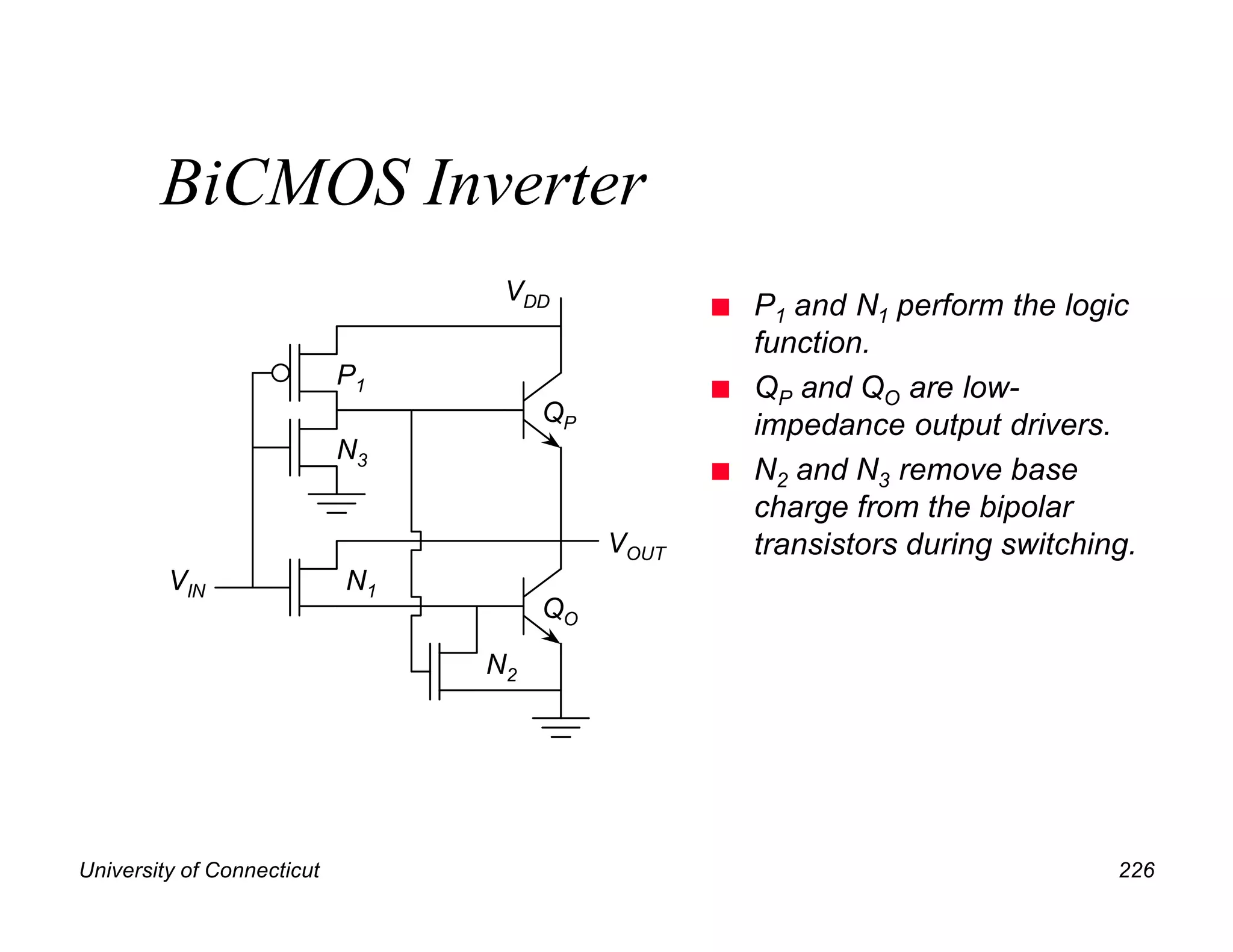
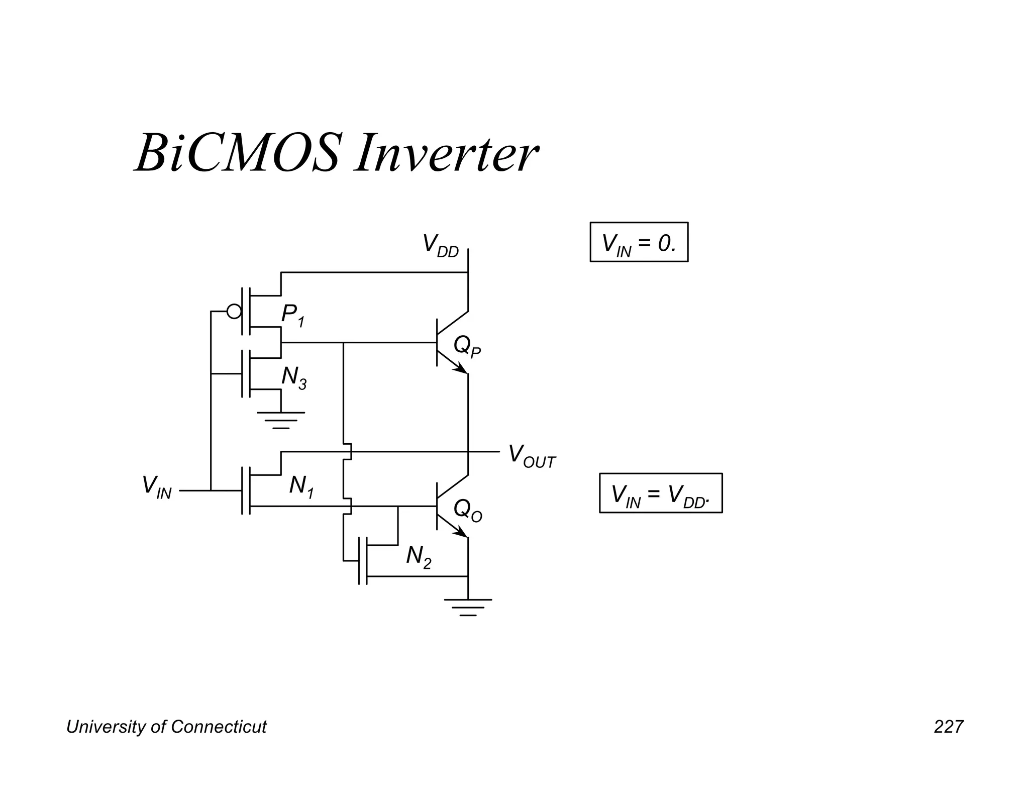
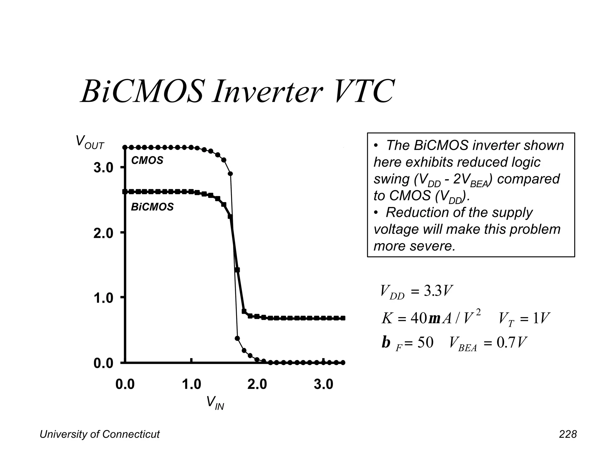
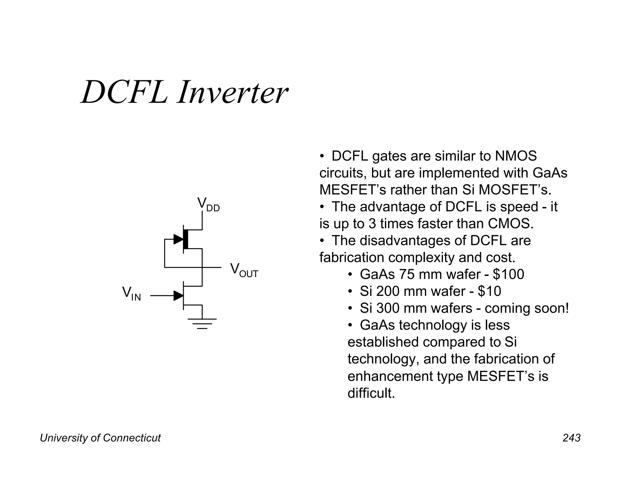
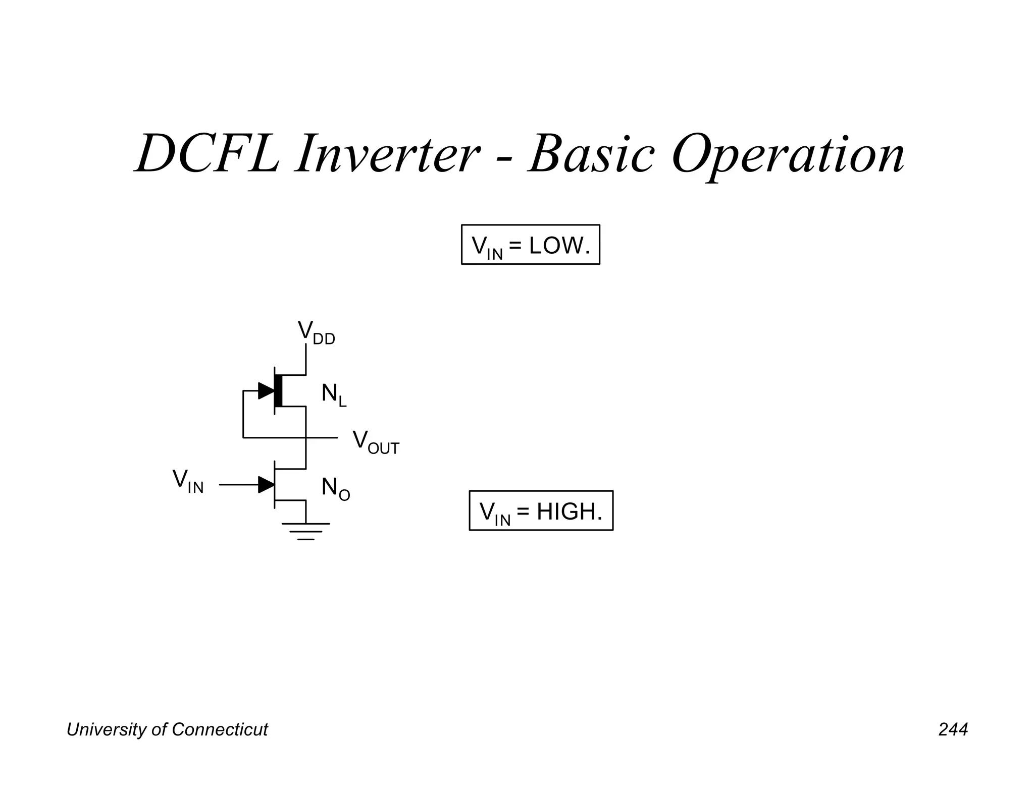
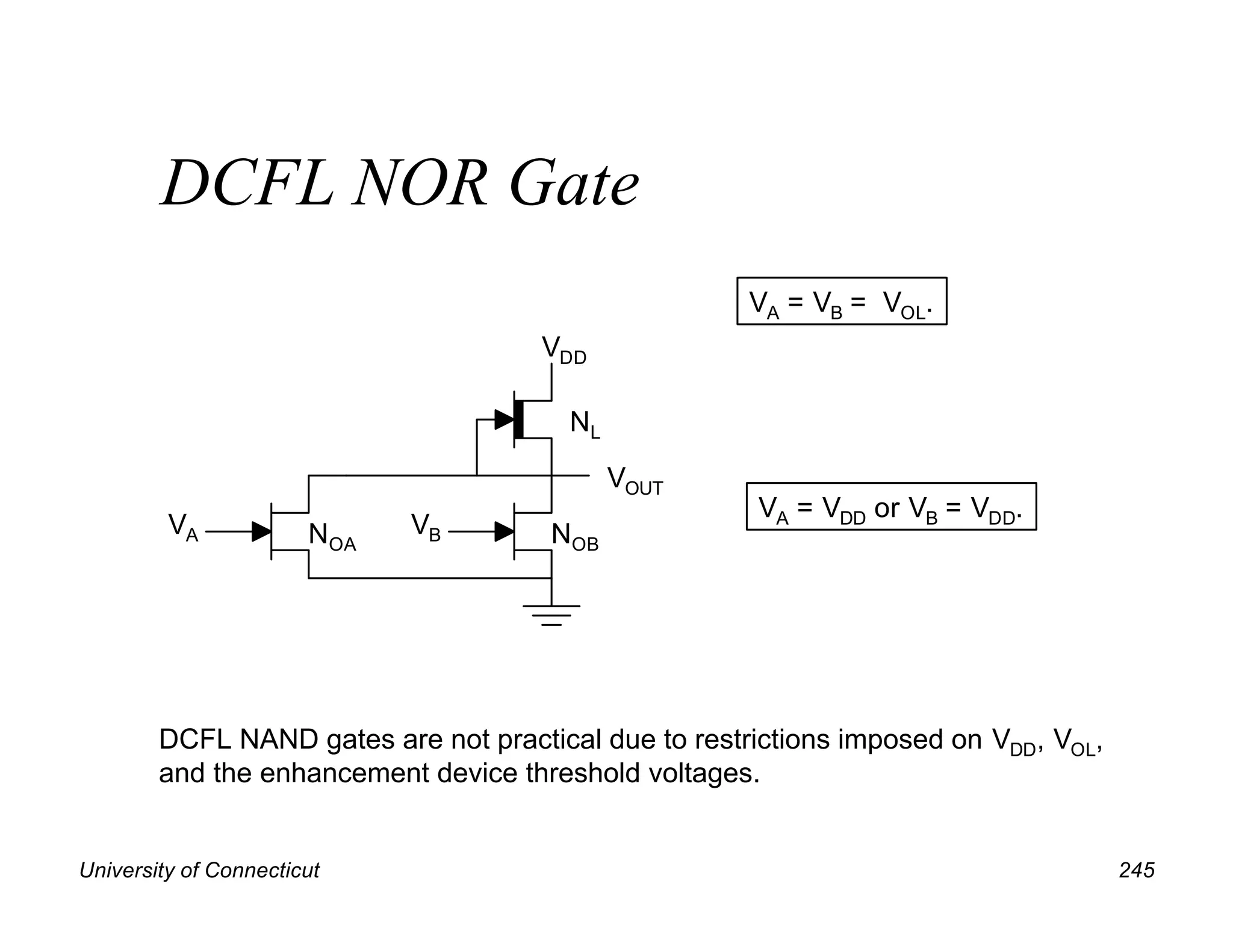
This document discusses BiCMOS and DCFL logic circuitry as alternatives to traditional CMOS. It provides details on the operation and advantages/disadvantages of BiCMOS inverters, NAND gates, and other circuits. DCFL using gallium arsenide is also examined and compared to CMOS. While BiCMOS and DCFL provide higher speeds, they have higher fabrication complexity and costs compared to CMOS. Examples of applications where the extra speed justifies the costs are mentioned.
This presentation discusses the basics of Pass Transistor Logic, its advantages, limitation and finally implementation of Boolean functions/Combinational Logic circuits using Pass Transistor Logic.
Cmos fabrication is a part of semiconductor electronics that deals with the designing and fabrication process with NMOS and Cmos and other processes like Twin tub techniques and etc.
This presentation has given a brief introduction and working of CMOS Logic Structures which includes MOS logic, CMOS logic, CMOS logic structure, CMOS complementary logic, pass transistor logic, bi CMOS logic, pseudo –nMOS logic, CMOS domino logic, Cascode Voltage Switch Logic(CVSL), clocked CMOS logic(c²mos), dynamic CMOS logic
The CMOS VLSI DESIGN PPT had the complete vision on VLSI Design styles in chip fabrication. It can give a good amount of knowledge to the students who needs VLSI Design
SHORT-CHANNEL EFFECTS
A MOSFET is considered to be short when the channel length ‘L’ is the same order of magnitude as the depletion-layer widths (xdD, xdS). The potential distribution in the channel now depends upon both, transverse field Ex, due to gate bias and also on the longitudinal field Ey, due to drain bias When the Gate channel length <<1 m, short channel effect becomes important .
This leads to many
undesirable effects in MOSFET.
The short-channel effects are attributed to two physical phenomena:
A) The limitation imposed on electron drift characteristics in the channel,
B) The modification of the threshold voltage due to the shortening channel length.
In particular five different short-channel effects can be distinguished:
1. Drain-induced barrier lowering and “Punch through”
2. Surface scattering
3. Velocity saturation
4. Impact ionization
5. Hot electrons
I have prepared it to create an understanding of delay modeling in VLSI.
Regards,
Vishal Sharma
Doctoral Research Scholar,
IIT Indore
vishalfzd@gmail.com
Here are the all short channel effects that you require.It consist of:-
Drain Induced Barrier Lowering
Hot electron Effect
Impact Ionization
Surface Scattering
Velocity saturation
CMOS FABRICATION
For less power dissipation requirement CMOS technology is used for implementing transistors. If we require a faster circuit then transistors are implemented over IC using BJT . Fabrication of CMOS transistors as IC’s can be done in three different methods.
The N-well / P-well technology, where n-type diffusion is done over a p-type substrate or p-type diffusion is done over n-type substrate respectively.
P-WELL PROCESS
The fabrication steps of p well process are same as that of an n-well process except that instead of n-well a p-well is implanted . The process steps involved in p-well process are shown in Figure below. The process starts with the n type substrate
Introduction to CMOS VLSI Design:
This Presentations is design in way to provide basic summary of CMOS Vlsi design
This Presentation is Made at Eutectics.blogspot.in
the following is the structure of presentation :
2: Outline
3: Introduction
4: MOS capacitor
5: Terminal Voltage
6: nMOS Cutoff
7: nMOS Linear
8: nMOS Saturation
9: I-V Characteristics
10 : Channel Charge
11: Carrier velocity
12: nMOS Linear I-V
13: nMOS Saturation
14: nMOS I-V Summary
15: Example
16: pMOS I-V
17: Capacitance
18: Gate Capacitance
19: Diffusion Capacitane
20: Pass Transistor
21: Pass transistor ckts
22: Effective Resistance
23: RC Delay Model
24: RC values
25: Inverter Delay Estimate
Cosmetic shop management system project report.pdfKamal Acharya
Buying new cosmetic products is difficult. It can even be scary for those who have sensitive skin and are prone to skin trouble. The information needed to alleviate this problem is on the back of each product, but it's thought to interpret those ingredient lists unless you have a background in chemistry.
Instead of buying and hoping for the best, we can use data science to help us predict which products may be good fits for us. It includes various function programs to do the above mentioned tasks.
Data file handling has been effectively used in the program.
The automated cosmetic shop management system should deal with the automation of general workflow and administration process of the shop. The main processes of the system focus on customer's request where the system is able to search the most appropriate products and deliver it to the customers. It should help the employees to quickly identify the list of cosmetic product that have reached the minimum quantity and also keep a track of expired date for each cosmetic product. It should help the employees to find the rack number in which the product is placed.It is also Faster and more efficient way.
Hybrid optimization of pumped hydro system and solar- Engr. Abdul-Azeez.pdffxintegritypublishin
Advancements in technology unveil a myriad of electrical and electronic breakthroughs geared towards efficiently harnessing limited resources to meet human energy demands. The optimization of hybrid solar PV panels and pumped hydro energy supply systems plays a pivotal role in utilizing natural resources effectively. This initiative not only benefits humanity but also fosters environmental sustainability. The study investigated the design optimization of these hybrid systems, focusing on understanding solar radiation patterns, identifying geographical influences on solar radiation, formulating a mathematical model for system optimization, and determining the optimal configuration of PV panels and pumped hydro storage. Through a comparative analysis approach and eight weeks of data collection, the study addressed key research questions related to solar radiation patterns and optimal system design. The findings highlighted regions with heightened solar radiation levels, showcasing substantial potential for power generation and emphasizing the system's efficiency. Optimizing system design significantly boosted power generation, promoted renewable energy utilization, and enhanced energy storage capacity. The study underscored the benefits of optimizing hybrid solar PV panels and pumped hydro energy supply systems for sustainable energy usage. Optimizing the design of solar PV panels and pumped hydro energy supply systems as examined across diverse climatic conditions in a developing country, not only enhances power generation but also improves the integration of renewable energy sources and boosts energy storage capacities, particularly beneficial for less economically prosperous regions. Additionally, the study provides valuable insights for advancing energy research in economically viable areas. Recommendations included conducting site-specific assessments, utilizing advanced modeling tools, implementing regular maintenance protocols, and enhancing communication among system components.
Overview of the fundamental roles in Hydropower generation and the components involved in wider Electrical Engineering.
This paper presents the design and construction of hydroelectric dams from the hydrologist’s survey of the valley before construction, all aspects and involved disciplines, fluid dynamics, structural engineering, generation and mains frequency regulation to the very transmission of power through the network in the United Kingdom.
Author: Robbie Edward Sayers
Collaborators and co editors: Charlie Sims and Connor Healey.
(C) 2024 Robbie E. Sayers
Sachpazis:Terzaghi Bearing Capacity Estimation in simple terms with Calculati...Dr.Costas Sachpazis
Terzaghi's soil bearing capacity theory, developed by Karl Terzaghi, is a fundamental principle in geotechnical engineering used to determine the bearing capacity of shallow foundations. This theory provides a method to calculate the ultimate bearing capacity of soil, which is the maximum load per unit area that the soil can support without undergoing shear failure. The Calculation HTML Code included.
Final project report on grocery store management system..pdfKamal Acharya
In today’s fast-changing business environment, it’s extremely important to be able to respond to client needs in the most effective and timely manner. If your customers wish to see your business online and have instant access to your products or services.
Online Grocery Store is an e-commerce website, which retails various grocery products. This project allows viewing various products available enables registered users to purchase desired products instantly using Paytm, UPI payment processor (Instant Pay) and also can place order by using Cash on Delivery (Pay Later) option. This project provides an easy access to Administrators and Managers to view orders placed using Pay Later and Instant Pay options.
In order to develop an e-commerce website, a number of Technologies must be studied and understood. These include multi-tiered architecture, server and client-side scripting techniques, implementation technologies, programming language (such as PHP, HTML, CSS, JavaScript) and MySQL relational databases. This is a project with the objective to develop a basic website where a consumer is provided with a shopping cart website and also to know about the technologies used to develop such a website.
This document will discuss each of the underlying technologies to create and implement an e- commerce website.
About
Indigenized remote control interface card suitable for MAFI system CCR equipment. Compatible for IDM8000 CCR. Backplane mounted serial and TCP/Ethernet communication module for CCR remote access. IDM 8000 CCR remote control on serial and TCP protocol.
• Remote control: Parallel or serial interface.
• Compatible with MAFI CCR system.
• Compatible with IDM8000 CCR.
• Compatible with Backplane mount serial communication.
• Compatible with commercial and Defence aviation CCR system.
• Remote control system for accessing CCR and allied system over serial or TCP.
• Indigenized local Support/presence in India.
• Easy in configuration using DIP switches.
Technical Specifications
Indigenized remote control interface card suitable for MAFI system CCR equipment. Compatible for IDM8000 CCR. Backplane mounted serial and TCP/Ethernet communication module for CCR remote access. IDM 8000 CCR remote control on serial and TCP protocol.
Key Features
Indigenized remote control interface card suitable for MAFI system CCR equipment. Compatible for IDM8000 CCR. Backplane mounted serial and TCP/Ethernet communication module for CCR remote access. IDM 8000 CCR remote control on serial and TCP protocol.
• Remote control: Parallel or serial interface
• Compatible with MAFI CCR system
• Copatiable with IDM8000 CCR
• Compatible with Backplane mount serial communication.
• Compatible with commercial and Defence aviation CCR system.
• Remote control system for accessing CCR and allied system over serial or TCP.
• Indigenized local Support/presence in India.
Application
• Remote control: Parallel or serial interface.
• Compatible with MAFI CCR system.
• Compatible with IDM8000 CCR.
• Compatible with Backplane mount serial communication.
• Compatible with commercial and Defence aviation CCR system.
• Remote control system for accessing CCR and allied system over serial or TCP.
• Indigenized local Support/presence in India.
• Easy in configuration using DIP switches.
Water scarcity is the lack of fresh water resources to meet the standard water demand. There are two type of water scarcity. One is physical. The other is economic water scarcity.
2. University of Connecticut 225
BiCMOS - Best of Both Worlds?
n CMOS circuitry exhibits very low power dissipation, but
n Bipolar logic achieves higher speed and current drive capability.
n BiCMOS achieves low standby dissipation like CMOS, but high
speed and current drive capability like TTL and ECL.
n The disadvantage of BiCMOS is fabrication complexity (up to 30
masking steps, compared to about 20 for bipolar logic or
CMOS). This translates into higher cost and longer design
cycles.
n Notable examples of the BiCMOS technology are the Intel P6
(a.k.a. Pentium Pro) which appeared in 1996, and its successor
the P7.
$
3. University of Connecticut 226
BiCMOS Inverter
n P1 and N1 perform the logic
function.
n QP and QO are low-
impedance output drivers.
n N2 and N3 remove base
charge from the bipolar
transistors during switching.
QP
QO
P1
N3
N1
N2
VOUT
VIN
VDD
5. University of Connecticut 228
BiCMOS Inverter VTC
• The BiCMOS inverter shown
here exhibits reduced logic
swing (VDD - 2VBEA) compared
to CMOS (VDD).
• Reduction of the supply
voltage will make this problem
more severe.
0.0
1.0
2.0
3.0
0.0 1.0 2.0 3.0
VIN
VOUT
CMOS
BiCMOS
V V
K A V V V
V V
DD
T
F BEA
=
= =
= =
3 3
40 1
50 0 7
2
.
/
.
µ
β
6. University of Connecticut 229
BiCMOS NAND Gate
QP
QO
PA
NB3
NA1
N2
VOUT
VA
VDD
VB
PB
NB1
NA3
With both inputs high:
With VA high, VB low:
7. University of Connecticut 230
How Fast is BICMOS?
n For highly-capacitive off-chip
loads, fast switching is possible
due to the high current driving
capability of the bipolar
transistors. The speed is limited
by the parasitic capacitances of
the QP, which must be driven by
the P1 - N3 CMOS circuit.
n For on-chip loads presenting very
little capacitance, BiCMOS offers
no advantage if
CL < CBCP
n BiCMOS integrated circuits are
really CMOS on the inside!
QP
QO
P1
N3
N1
N2
VOUT
VIN
VDD
8. University of Connecticut 231
BiCMOS Applications
n Modern BiCMOS, invented by Intel, hit the market in 1992.
n Ever-increasing clock frequencies on motherboards of PC’s and
workstations may require that the VLSI / ULSI chips be made in
BiCMOS. (Witness the Intel, AMD, and Cyrix µP chips.)
n Central Processing Units (CPU’s) of “minisupercomputers” can
be implemented in BiCMOS, with packing density and
dissipation advantages over ECL. (e.g., the Cray Research
“Baby Cray” J916 Computer)
n TTL will soldier on in motherboard SSI and MSI applications,
where BiCMOS does not boast an advantage.
n But … the BiCMOS party may be over when supply
voltages drop below 1.8 V. BJT’s have a fixed turn-on
voltage; MOSFET thresholds can be reduced to at least
0.3V for room temperature operation.
9. University of Connecticut 232
The Problem with BiCMOS
n For standard BiCMOS, the logic swing is VDD - 2VBEA.
n Supply voltages are continually being reduced, because
n When VDD is reduced to 1.8V, standard BiCMOS will provide a
logic swing of only 0.4V; this isn’t acceptable! We can provide
shunt elements which increase the voltage swing of BiCMOS,
but …
n Turning off the BJT’s isn’t the answer! If the supply voltage is
1.8V, the BJT’s can only conduct for
n In this case the BJT’s can not effectively boost the switching
speed.
P C V
L DD
≈ 2
0 7 11
. .
V V V
OUT
≤ ≤
10. University of Connecticut 233
Full-Rail BiCMOS Inverter w/
Resistive Shunts
QP
QO
P1
N1
VOUT
VIN
VDD
R1
R2
• This BiCMOS design provides a
rail-to-rail voltage swing.
• For VOUT < VBEA, N1 and R2
conduct, bringing VOL all the way to
0.
• For VBEA < VOUT < VDD - VBEA, one
or both BJT’s conducts.
• For VDD - VBEA < VOUT, P1 and R1
conduct, bringing VOH all the way to
VDD.
• It is not practical to fabricate this
circuit with resistors, but a similar
circuit can be made using an active
shunt for QO.
11. University of Connecticut 234
BiCMOS Inverter w/ Active Shunt
QP
QO
P1
N1
VOUT
VIN
VDD • This BiCMOS design provides a
voltage swing of VDD - VBEA.
• For VOUT < VBEA, N3 and N2
conduct, bringing VOL all the way to
0.
• For VBEA < VOUT < VDD - VBEA, one
or both BJT’s conducts.
• The base-emitter junction of QP is
not shunted, so VOH = VDD - VBEA.
N2
N3
12. University of Connecticut 235
Full Rail BiCMOS Inverter w/
Paralleled CMOS Output
QP
QO
P1
N3
N1
N2
VOUT
VIN
VDD
NO
PO
• The parallel CMOS
inverter provides rail-to-rail
operation.
• For VOUT < VBEA, NO
conducts, bringing VOL all
the way to 0.
• For VBEA < VOUT < VDD -
VBEA, one or both BJT’s
conducts.
• For VDD - VBEA < VOUT, PO
conducts, bringing VOH all
the way to VDD.
14. University of Connecticut 237
CMOS - Single Stage
VDD = 1.8V
VIN
VT = -0.6V
2.2µ m/ 0.5µ m
VT = 0.6V
0.9µ m/ 0.5µ m
tP =
VOUT
CL
2
'
2
'
/
200
/
80
100
V
A
k
V
A
k
Angstroms
t
N
P
OX
µ
µ
=
=
=
=
A
15. University of Connecticut 238
CMOS - Single Stage / 50pF
VDD = 1.8V
VIN
VT = -0.6V
2.2µ m/ 0.5µ m
VT = 0.6V
0.9µ m/ 0.5µ m
VOUT
50pF
=
=
N
P
K
K
=
P
t
16. University of Connecticut 239
CMOS - Three Stages / 50pF
VDD = 1.8V
VIN
2.2/ 0.5
VOUT
50pF
=
P
t
0.9/ 0.5
11/ 0.5
4.5/ 0.5
55/ 0.5
22/ 0.5
=
=
=
1
1
1
P
L
t
C
K
=
=
=
2
2
2
P
L
t
C
K
=
=
=
3
3
3
P
L
t
C
K
17. University of Connecticut 240
CMOS - Six Stages / 50pF
VDD = 1.8V
VIN
2.2/ 0.5
0.9/ 0.5
11/ 0.5
4.5/ 0.5
55/ 0.5
22/ 0.5
=
=
=
1
1
1
P
L
t
C
K
=
=
=
2
2
2
P
L
t
C
K
=
=
=
3
3
3
P
L
t
C
K
WIRED
TO THE
NEXT
PAGE!
18. University of Connecticut 241
CMOS - Six Stages / 50pF
VDD = 1.8V
275/ 0.5
VOUT
50pF
=
P
t
110/ 0.5
1375/ 0.5
550/ 0.5
6875/ 0.5
2750/ 0.5
=
=
=
5
5
5
P
L
t
C
K
=
=
=
6
6
6
P
L
t
C
K
WIRED
FROM THE
PREVIOUS
PAGE!
=
=
=
4
4
4
P
L
t
C
K
20. University of Connecticut 243
DCFL Inverter
VOUT
VIN
VDD
• DCFL gates are similar to NMOS
circuits, but are implemented with GaAs
MESFET’s rather than Si MOSFET’s.
• The advantage of DCFL is speed - it
is up to 3 times faster than CMOS.
• The disadvantages of DCFL are
fabrication complexity and cost.
• GaAs 75 mm wafer - $100
• Si 200 mm wafer - $10
• Si 300 mm wafers - coming soon!
• GaAs technology is less
established compared to Si
technology, and the fabrication of
enhancement type MESFET’s is
difficult.
21. University of Connecticut 244
DCFL Inverter - Basic Operation
VOUT
VIN
VDD
NL
NO
VIN = LOW.
VIN = HIGH.
22. University of Connecticut 245
DCFL NOR Gate
VOUT
VB
VDD
NL
NOB
VA NOA
VA = VB = VOL.
VA = VDD or VB = VDD.
DCFL NAND gates are not practical due to restrictions imposed on VDD, VOL,
and the enhancement device threshold voltages.
23. University of Connecticut 246
Buffered DCFL NOR Gate
VB
VDD
VA
The added source follower provides a low-impedance output driver for off-chip
loads.
VOUT
VB
VA
24. University of Connecticut 247
DCFL Characteristics
Compare the 1999 state-of-the art for GaAs DCFL and Si CMOS:
GaAs DCFL vs. Si CMOS: 0.25 µm technology
propagation delay
dissipation
SRAM embedded in VLSI
GaAs DCFL
35 ps
30 µW (DC)
32 kB
Si CMOS
75 ps
1 µW / MHz
128 kB
• GaAs exhibits higher electron mobility than Si.
• Due to the GaAs electron velocity characteristic, DCFL can operate
at a reduced supply voltage without a penalty in switching speed.
25. University of Connecticut 248
DCFL Applications
n For a given minimum linewidth, GaAs DCFL circuitry is about 2
to 3 times faster than Si CMOS because of the difference in
electron mobilities.
n The extra speed comes at a premium, because GaAs
technology is less developed and DCFL is expensive.
n DCFL applications are at the high end, where the extra cost can
be justified. Examples are the Cray Y-MP and the Vitesse
Semiconductor GaAs microprocessor, which boasts 1.2 M
transistors [see Ira Deyhimy, “Gallium Arsenide Joins the Giants,” IEEE
Spectrum, pp. 33-40, February 1995].
n At the present time, the area of fastest growth for GaAs DCFL is
communications.
n A factor of three isn’t much, though, when you consider the rapid
advancement of Si CMOS / BiCMOS technology.