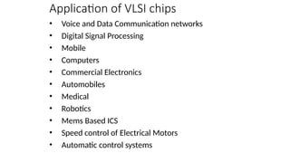
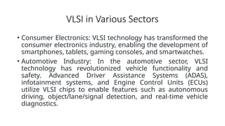
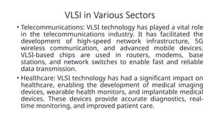
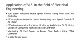
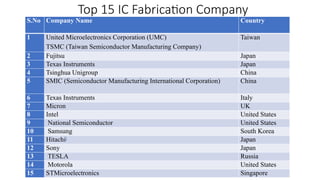
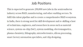
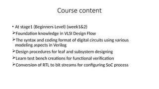
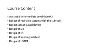
Internship Training Program
on
FPGA DESIGN TECHNIQUES USING
Quartus/Xilinx FRONT END TOOL
Presented by
Dr.R.UMA
PUDUCHERRY INSTITUTE OF EDUCATION
AND DEVELOPMENT STUDIES
(PIEDS)
(A Public Charitable Trust Registered Under Indian Trusts Act. 1882)
Objectives of the Trust
• To focus on promotional and developmental activities in the
education and socio economic spheres
• To provide training, teaching, assessment, research and extension to
sub serve the goals of National Educational Policy (NEP)
Internship Program
• The internship program in the VLSI domain provides various
benefits for engineering students who want to broaden
their chances of getting careers in core industries.
• This internship program is a preserved training designed to
render the practical experience
• To increase the value of theoretical knowledge than regular
curriculum
• Explore career alternatives prior to graduation.
• Integrate theory and practice.
• Training in specific domains both programming and
configuration of device or application.
• Provide an opportunity to get work in real-time project
Video TSMC Manufacturing Process
AIM/OBJECTIVES
AIM
To provide a foundation for intermediate knowledge
and exploration skills in Xilinx ISE tool and Quartus
using Verilog HDL
OBJECTIVES
1. Understanding the concept of VLSI design
2. Understanding the fabrication process
3. Design methodology in FPGA and ASIC
4. Learning circuit design in Verilog HDL
Tools
• FPGA
1. Xilinx
2. Quartus
• ASIC
Microwind
VLSI
• Very-large-scale integration (VLSI) is the process of
creating an integrated circuit (IC) by combining
thousands of transistors into a single chip.
• VLSI began in the 1970s when complex
semiconductor and communication technologies
were being developed. The microprocessor is a VLSI
device
Levels of integration
Depending upon the number of components (Transistors) to be integrated, they were categorized as
SSI, MSI, LSI, VLSI, ULSI & GSI.
Small Scale Integration (SSI):
In this Technology, 1-100 Transistors were fabricated on a single chip. eg Gates , Flipflops.
Medium Scale Integration (MSI):
Using this Technology, 100-1000 number of Transistors could be integrated on a single chip. eg 4 bit
Microprocessors.
Large Scale Integration
In this Technology, 1000-10000 Transistors could be integrated on a single chip. eg 8 bit
Microprocessors, RAM, ROM
Very Large Scale Integration(VLSI):
In this Technology, 10000-1 Million Transistors could be accommodated. Eg 16-32 bit
Microprocessors.
Ultra Large Scale Integration(ULSI):
In this Technology, 1 Million-10 Million Transistors could be accommodated. Eg Special Purpose
Registers.
Giant Scale Integration (GSI):
In this Technology more than 10 Million Transistors could be accommodated. Eg Embedded Systems.
Advantages of VLSI Technology
• Reduces the Size of Circuits.
• Reduces the effective cost of the devices.
• Increases the Operating speed of circuits
• Requires less power than Discrete components.
• Higher Reliability
• Occupies a relatively smaller area.
Application of VLSI chips
• Voice and Data Communication networks
• Digital Signal Processing
• Mobile
• Computers
• Commercial Electronics
• Automobiles
• Medical
• Robotics
• Mems Based ICS
• Speed control of Electrical Motors
• Automatic control systems
VLSI in Various Sectors
• Consumer Electronics: VLSI technology has transformed the
consumer electronics industry, enabling the development of
smartphones, tablets, gaming consoles, and smartwatches.
• Automotive Industry: In the automotive sector, VLSI
technology has revolutionized vehicle functionality and
safety. Advanced Driver Assistance Systems (ADAS),
infotainment systems, and Engine Control Units (ECUs)
utilize VLSI chips to enable features such as autonomous
driving, object/lane/signal detection, and real-time vehicle
diagnostics.
VLSI in Various Sectors
• Telecommunications: VLSI technology has played a vital role
in the telecommunications industry. It has facilitated the
development of high-speed network infrastructure, 5G
wireless communication, and advanced mobile devices.
VLSI-based chips are used in routers, modems, base
stations, and network switches to enable fast and reliable
data transmission.
• Healthcare: VLSI technology has had a significant impact on
healthcare, enabling the development of medical imaging
devices, wearable health monitors, and implantable medical
devices. These devices provide accurate diagnostics, real-
time monitoring, and improved patient care.
Application of VLSI in the field of Electrical
Engineering
• VLSI Based Induction Motor Speed Control Using Auto Tune PID
Controller
• FPGA Implementation For Speed Monitoring And Speed Control Of
AC Motor
• FPGA Implementation For Speed Monitoring And Control Of DC Motor
Using Soft Computing Technique Based Controller
• Monitoring Of Fuel Supply In Power Plant Boilers Using FPGA
Controller
• In solar Power plants
India’s Semiconductor Sector
The Indian government approved the establishment of three new
semiconductor manufacturing facilities on February 29-2023
• Semiconductor Fab (fabrication facility)– at Dholera, Gujarat
Tata Electronics Private Limited (TEPL) will collaborate with Powerchip
Semiconductor Manufacturing Corp (PSMC), Taiwan, to establish a
semiconductor fab in Dholera, Gujarat, with an investment of INR 9100 billion
• Semiconductor ATMP (Assembly, Test, Marking and Packaging) unit – at
Morigaon, Assam
Tata Semiconductor Assembly and Test Pvt Ltd (TSAT) will set up a
semiconductor unit in Morigaon, Assam, with an investment of INR 2700
million (US$325.99 million).
• Semiconductor ATMP unit for specialized chips – at Sanand, Gujarat
CG Power, in partnership with Renesas Electronics Corporation, Japan, and
Stars Microelectronics, Thailand, will establish a semiconductor unit in
Sanand, Gujarat, with an investment of INR 760 million (US$91.63 million).
Top 15 IC Fabrication Company
S.No Company Name Country
1 United Microelectronics Corporation (UMC)
TSMC (Taiwan Semiconductor Manufacturing Company)
Taiwan
2 Fujitsu Japan
3 Texas Instruments Japan
4 Tsinghua Unigroup China
5 SMIC (Semiconductor Manufacturing International Corporation) China
6 Texas Instruments Italy
7 Micron UK
8 Intel United States
9 National Semiconductor United States
10 Samsung South Korea
11 Hitachi[
Japan
12 Sony Japan
13 TESLA Russia
14 Motorola United States
15 STMicroelectronics Singapore
Job Positions
Course content
• At stage1 (Beginners Level) (week1&2)
Foundation knowledge in VLSI Design Flow
The syntax and coding format of digital circuits using various
modeling aspects in Verilog
Design procedures for leaf and subsystem designing
Learn test bench creations for functional verification
Conversion of RTL to bit streams for configuring SoC process
Course Content
• At stage2 (Intermediate Level) (week3)
• Design of real-time systems with the sub-cells
• Design sensor-based device
• Design of SPI
• Design of I2C
• Design of Vending machine
• Design of USART

Internship Training Program on FPGA DESIGN TECHNIQUES USING Quartus/Xilinx FRONT END TOOL

  • 1.
    Internship Training Program on FPGADESIGN TECHNIQUES USING Quartus/Xilinx FRONT END TOOL Presented by Dr.R.UMA
  • 2.
    PUDUCHERRY INSTITUTE OFEDUCATION AND DEVELOPMENT STUDIES (PIEDS) (A Public Charitable Trust Registered Under Indian Trusts Act. 1882)
  • 3.
    Objectives of theTrust • To focus on promotional and developmental activities in the education and socio economic spheres • To provide training, teaching, assessment, research and extension to sub serve the goals of National Educational Policy (NEP)
  • 4.
    Internship Program • Theinternship program in the VLSI domain provides various benefits for engineering students who want to broaden their chances of getting careers in core industries. • This internship program is a preserved training designed to render the practical experience • To increase the value of theoretical knowledge than regular curriculum • Explore career alternatives prior to graduation. • Integrate theory and practice. • Training in specific domains both programming and configuration of device or application. • Provide an opportunity to get work in real-time project
  • 5.
  • 6.
    AIM/OBJECTIVES AIM To provide afoundation for intermediate knowledge and exploration skills in Xilinx ISE tool and Quartus using Verilog HDL OBJECTIVES 1. Understanding the concept of VLSI design 2. Understanding the fabrication process 3. Design methodology in FPGA and ASIC 4. Learning circuit design in Verilog HDL
  • 7.
    Tools • FPGA 1. Xilinx 2.Quartus • ASIC Microwind
  • 8.
    VLSI • Very-large-scale integration(VLSI) is the process of creating an integrated circuit (IC) by combining thousands of transistors into a single chip. • VLSI began in the 1970s when complex semiconductor and communication technologies were being developed. The microprocessor is a VLSI device
  • 9.
    Levels of integration Dependingupon the number of components (Transistors) to be integrated, they were categorized as SSI, MSI, LSI, VLSI, ULSI & GSI. Small Scale Integration (SSI): In this Technology, 1-100 Transistors were fabricated on a single chip. eg Gates , Flipflops. Medium Scale Integration (MSI): Using this Technology, 100-1000 number of Transistors could be integrated on a single chip. eg 4 bit Microprocessors. Large Scale Integration In this Technology, 1000-10000 Transistors could be integrated on a single chip. eg 8 bit Microprocessors, RAM, ROM Very Large Scale Integration(VLSI): In this Technology, 10000-1 Million Transistors could be accommodated. Eg 16-32 bit Microprocessors. Ultra Large Scale Integration(ULSI): In this Technology, 1 Million-10 Million Transistors could be accommodated. Eg Special Purpose Registers. Giant Scale Integration (GSI): In this Technology more than 10 Million Transistors could be accommodated. Eg Embedded Systems.
  • 10.
    Advantages of VLSITechnology • Reduces the Size of Circuits. • Reduces the effective cost of the devices. • Increases the Operating speed of circuits • Requires less power than Discrete components. • Higher Reliability • Occupies a relatively smaller area.
  • 11.
    Application of VLSIchips • Voice and Data Communication networks • Digital Signal Processing • Mobile • Computers • Commercial Electronics • Automobiles • Medical • Robotics • Mems Based ICS • Speed control of Electrical Motors • Automatic control systems
  • 12.
    VLSI in VariousSectors • Consumer Electronics: VLSI technology has transformed the consumer electronics industry, enabling the development of smartphones, tablets, gaming consoles, and smartwatches. • Automotive Industry: In the automotive sector, VLSI technology has revolutionized vehicle functionality and safety. Advanced Driver Assistance Systems (ADAS), infotainment systems, and Engine Control Units (ECUs) utilize VLSI chips to enable features such as autonomous driving, object/lane/signal detection, and real-time vehicle diagnostics.
  • 13.
    VLSI in VariousSectors • Telecommunications: VLSI technology has played a vital role in the telecommunications industry. It has facilitated the development of high-speed network infrastructure, 5G wireless communication, and advanced mobile devices. VLSI-based chips are used in routers, modems, base stations, and network switches to enable fast and reliable data transmission. • Healthcare: VLSI technology has had a significant impact on healthcare, enabling the development of medical imaging devices, wearable health monitors, and implantable medical devices. These devices provide accurate diagnostics, real- time monitoring, and improved patient care.
  • 14.
    Application of VLSIin the field of Electrical Engineering • VLSI Based Induction Motor Speed Control Using Auto Tune PID Controller • FPGA Implementation For Speed Monitoring And Speed Control Of AC Motor • FPGA Implementation For Speed Monitoring And Control Of DC Motor Using Soft Computing Technique Based Controller • Monitoring Of Fuel Supply In Power Plant Boilers Using FPGA Controller • In solar Power plants
  • 15.
    India’s Semiconductor Sector TheIndian government approved the establishment of three new semiconductor manufacturing facilities on February 29-2023 • Semiconductor Fab (fabrication facility)– at Dholera, Gujarat Tata Electronics Private Limited (TEPL) will collaborate with Powerchip Semiconductor Manufacturing Corp (PSMC), Taiwan, to establish a semiconductor fab in Dholera, Gujarat, with an investment of INR 9100 billion • Semiconductor ATMP (Assembly, Test, Marking and Packaging) unit – at Morigaon, Assam Tata Semiconductor Assembly and Test Pvt Ltd (TSAT) will set up a semiconductor unit in Morigaon, Assam, with an investment of INR 2700 million (US$325.99 million). • Semiconductor ATMP unit for specialized chips – at Sanand, Gujarat CG Power, in partnership with Renesas Electronics Corporation, Japan, and Stars Microelectronics, Thailand, will establish a semiconductor unit in Sanand, Gujarat, with an investment of INR 760 million (US$91.63 million).
  • 16.
    Top 15 ICFabrication Company S.No Company Name Country 1 United Microelectronics Corporation (UMC) TSMC (Taiwan Semiconductor Manufacturing Company) Taiwan 2 Fujitsu Japan 3 Texas Instruments Japan 4 Tsinghua Unigroup China 5 SMIC (Semiconductor Manufacturing International Corporation) China 6 Texas Instruments Italy 7 Micron UK 8 Intel United States 9 National Semiconductor United States 10 Samsung South Korea 11 Hitachi[ Japan 12 Sony Japan 13 TESLA Russia 14 Motorola United States 15 STMicroelectronics Singapore
  • 18.
  • 19.
    Course content • Atstage1 (Beginners Level) (week1&2) Foundation knowledge in VLSI Design Flow The syntax and coding format of digital circuits using various modeling aspects in Verilog Design procedures for leaf and subsystem designing Learn test bench creations for functional verification Conversion of RTL to bit streams for configuring SoC process
  • 20.
    Course Content • Atstage2 (Intermediate Level) (week3) • Design of real-time systems with the sub-cells • Design sensor-based device • Design of SPI • Design of I2C • Design of Vending machine • Design of USART