Downloaded 13 times
![Regu Archana Int. Journal of Engineering Research and Applications www.ijera.com
ISSN : 2248-9622, Vol. 4, Issue 10 ( Version 5), October 2014, pp.06-10
www.ijera.com 8 | P a g e
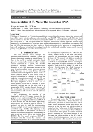
Fig. 5 - Master Receiver Mode
Fig. 6: Acknowledgement on the I2
C Bus
MAXIM DS1307:
The DS1307 supports a bi-directional, 2- wire
bus and data transmission protocol. The pin
assignment of DS1307 is given in Fig-6. The DS1307
operates as a slave on the 2- wire bus. Fig-7 shows
the interface connection of I2
C bus in Spartan 3E
with the DS1307 RTC chip.
Fig. 7: DS1307 connected to two wire data bus
V. SOFTWARE IMPLEMENTATION
I2
C master protocol is designed using VHDL
based on Finite State Machine (FSM). FSM is a
sequential circuit that uses a finite number of states to
keep track of its history of operations, and based on
history of operation and current input, determines the
next state. There are several states in obtaining the
result.
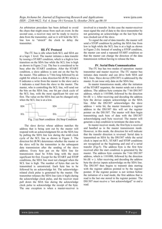
Algorithm
State 1: An idle condition: I2
C bus doesn’t
perform any operation. (SCL and SDA remains
high).
State 2: Start condition: master initiates data
transmission by providing START (SCL is high
and SDA is from high to low).
State 3: Slave address - write: master sends the
slave address-write (11010000) to the slave.
State 4: If the slave address matches with the
slave, it sends an acknowledgement bit in
response to the master.
State 5: 8 Bit Register Address[12] will be
transmitted to the slave. Again acknowledgement
is sent to the master by the slave.
State 6: Data to be transmitted is sent to the
slave by the master. After receiving the data,
slave acknowledges the master.
State 7: Stop condition: Slave sends a stop bit to
the master to terminate the communication (SCL
is high and SDA is from Low to high). For
performing read operation, write operation is
performed first and then read operation is done.
Slave address for read is 11010001. (State 7 will
not be performed for read operation)
State 8: Master transmits slave address for read
operation to the slave.
State 9: Master receives the data from the slave
and acknowledges the slave.
State 10: Master sends a STOP bit to terminate
the connection (SCL is high and SDA is from
Low to high).
Fig.8 shows the flowchart for I2
C master bus
communication with slave device. Fig-10 shows the
simulation result for DS1307. In DS1307, we have
activated only 4th order FIR filter for the given data
input and filter coefficients are applied and output is
observed. Generated square output is also observed
programmed in VHDL. Fig-11 shows the simulation](https://image.slidesharecdn.com/b410050610-141115044145-conversion-gate01/85/Implementation-of-I2C-Master-Bus-Protocol-on-FPGA-3-320.jpg)
![Regu Archana Int. Journal of Engineering Research and Applications www.ijera.com
ISSN : 2248-9622, Vol. 4, Issue 10 ( Version 5), October 2014, pp.06-10
www.ijera.com 10 | P a g e
protocol, I2
C Master (Master) transmits and receives
data to and from the DS1307 (Slave). So that any low
speed peripheral devices can be interfaced using I2
C
bus protocol as master. In future, this can be
implemented as real time clock in networks that
contains multiple masters and multiple slaves to
coordinate the entire system by clock synchronization
techniques.
REFERENCES
[1] I2
C Bus Specification, Philips
Semiconductor, version 2.1, January 2000.
[2] DS1307 64 x 8, Serial, I2
C Real Time
Clock, Maxim integrated, 2008.
[3] Prof. Jai Karan Singh et al “Design and
Implementation of I2
C master controller on
FPGA using VHDL,” IJET, Aug-Sep 2012.
[4] Raj Kamal, “Devices and Communication
Buses for Devices Network,” in Embedded
system: Architecture programming and
Design, Shalini Jha Ed. New Delhi, India:
Tata McGraw-Hill Education, 2008, pp.160-
165.
[5] Tim Wilmshurst, “Starting with Serial,” in
Designing Embedded
[6] Spartan-3A/3AN FPGA Starter Kit Board
User Guide, Xilinx, version 1.1, 2008.
[7] A.P.Godse, D.A.Godse, “Bus Standards,” in
Microprocessors and its Applications, 3rd
Ed. Pune, India: Technical publications,
2008.
[8] Systems with PIC Micro-controllers:
Principles and Applications, 2nd Ed.
Burlinton: Newnes, 2009, pp.307-327.
[9] Vincent Himpe, “Historical background of
I2
C,” in Mastering the I2
C Bus, Aachen,
Germany: Elektor Verlag publications,
2011.
[10] Pong P.Chu, “I/O Modules,” in FPGA
Prototyping by Verilog Examples: Xilinx
Spartan – 3 Version, New Delhi, India:
Wiley, 2008.](https://image.slidesharecdn.com/b410050610-141115044145-conversion-gate01/85/Implementation-of-I2C-Master-Bus-Protocol-on-FPGA-5-320.jpg)

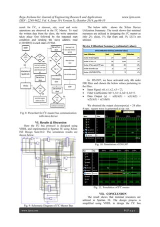
The paper discusses the implementation of the I2C (Inter-Integrated Circuit) master bus protocol on FPGA for interfacing a micro-controller with the DS1307 real-time clock. It details the design process using VHDL, including simulations and synthesis, demonstrating minimal resource utilization. The protocol allows communication between devices of varying speeds and can facilitate real-time clock synchronization in systems with multiple masters and slaves.


![Finite Element Simulation of Plasma Transferred ARC Welding [PTAW] of Structu...](https://cdn.slidesharecdn.com/ss_thumbnails/b410040611-141115042900-conversion-gate02-thumbnail.jpg?width=640&height=640&fit=bounds)


