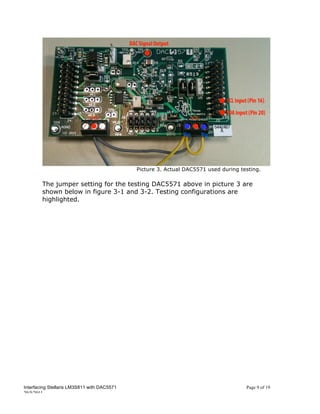
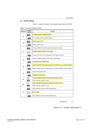
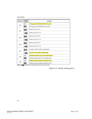
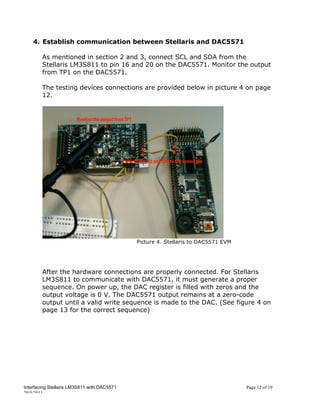
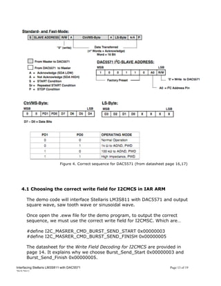
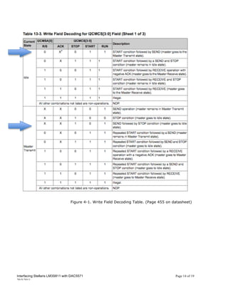
SlideShare a Scribd company logo
Interfacing Stellaris to DAC (I2C)
        Stellaris LM3S811 EVM to DAC5571 Data Converter EVM


                                              Abstract
The DAC5571 is a digital-to-analog converter (DAC). It provides a quick, easy
and low cost way to evaluate the functionality and performance of the high-
resolution as well as low-resolution I2C-input DACs. By interfacing the
DAC5571 with Stellaris LM3S811 through I2C, we can increase the range of
suitable application for Stellaris to another level.


Related code and additional information are provided.


                                              Contents

1. Introduction                                                                    2
2. Stellaris LM3S811 Inter-Integrated-Circuit (I2C) Interface                       2
   2.1 Block diagram                                                                3
   2.2 Functional description                                                       3
   2.2.1 I2C bus functional overview                                                3
   2.2.2 Start and stop condition                                                   4
   2.2.3 Data format with 7-bit address                                             4
   2.2.4 Data validity                                                              5
   2.2.5 Acknowledge                                                                5
   2.3 Evaluation board layout & Connection                                         6

3. DAC5571 EVM                                                                      8
   3.1 DAC configuration and setting                                                8

4. Establish communication between Stellaris and DAC5571                            12
   4.1 Choosing the correct write field for I2CMCS                                  13
   4.2 Functions used in demo code                                                  15

5. Reference                                                                         19


Interfacing Stellaris LM3S811 with DAC5571                                Page 1 of 19
20/5/2011
1. Introduction
       This application report will enhance the already feature-rich Stellaris
       LM3S811 microcontroller with DAC capability using DAC5571. The demo
       code will generate square wave, saw-tooth wave or Sinusoidal wave
       from the DAC5571 output. It offers the customer an easy solution and
       will definitely shorten the development process.


    2. Stellaris LM3S811 Inter-Integrated Circuit (I2C) Interface
       The Inter-Integrated Circuit (I2C) bus provides bi-directional data
       transfer through a two-wire design (a serial data line SDA and a serial
       clock line SCL), and interfaces to external I2C devices.

        The Stellaris I2C interface has the following features:
          • Devices on the I2C bus can be designated as either a master or
              slave
             ü Supports both sending and receiving data as either a master or
                 slave.
             ü Supports simultaneous master and slave operation.
          • Four I2C modes
             ü Master transmit
             ü Master receive
             ü Slave transmit
             ü Slave receive
          • Two transmission speed: Standard (100Kbps) and Fast (400Kbps)
          • Master and slave interrupt generation
             ü Master generates interrupts when a transmit or receive
                 operation completes (or aborts due to an error)
             ü Slave generates interrupts when data has been sent or
                 requested by a master
          • Master with arbitration and clock synchronization, multimaster
              support, and 7-bit addressing mode

     *The information on Stellaris LM3S811 I2C is mostly taken from Stellaris LM3SS811
     Datasheet. The information provided above and below should be enough to understand
     and use the I2C feature. For more information, please refer to section 13, page 437 from
     the datasheet.


Interfacing Stellaris LM3S811 with DAC5571                                          Page 2 of 19
20/5/2011
2.1 Block Diagram


                                                   Figure 2-1 I2C Block Diagram
     2.2 Functional Description

          I2C module is comprised of both master and slave functions, which are
          implemented as separate peripherals. For proper operation, the SDA
          and SCL pins must be connected to bi-directional open-drain pads. A
          typical I2C bus configuration is shown in Figure 2-2 on page 3.


                                                 Figure 2-2. I2C Bus Configuration

     2.2.1 I2C Bus Functional Overview

          The I2C bus uses only two signals: SDA and SCL, named I2CSDA and
          I2CSCL on Stellaris microcontrollers. SDA is the bi-directional serial
          data line and SCL is the bi-directional serial clock line. The bus is
          considered idle when both lines are High.

          Every transaction on the I2C bus is nine bits long, consisting of eight
          data bits and a single acknowledge bit. The number of bytes per
          transfer (defined as the time between a valid START and STOP
          condition, described in “START and STOP Conditions” on page 4) is
          unrestricted, but each byte has to be followed by an acknowledge bit,
          and data must be transferred MSB first. When a receiver cannot

Interfacing Stellaris LM3S811 with DAC5571                                   Page 3 of 19
20/5/2011
receive another complete byte, it can hold the clock line SCL Low and
          force the transmitter into a wait state. The data transfer continues
          when the receiver releases the clock SCL.


     2.2.2 Start and Stop Condition

          The protocol of the I2C bus defines two states to begin and end a
          transaction: START and STOP. A High-to-Low transition on the SDA line
          while the SCL is High is defined as a START condition, and a Low-to-
          High transition on the SDA line while SCL is High is defined as a STOP
          condition. The bus is considered busy after a START condition and free
          after a STOP condition. See Figure 2-3 on page 4.


                                                          Figure 2-3. START and STOP conditions

     2.2.3 Data format with 7-bit address

          Data transfers follow the format shown in Figure 2-4 on page 4. After
          the START condition, a slave address is sent. This address is 7-bits
          long followed by an eighth bit, which is a data direction bit (R/S bit in
          the I2CMSA register). A zero indicates a transmit operation (send),
          and a one indicates a request for data (receive). A data transfer is
          always terminated by a STOP condition generated by the master,
          however, a master can initiate communications with another device on
          the bus by generating a repeated START condition and addressing
          another slave without first generating a STOP condition. Various
          combinations of receive/send formats are then possible within a single
          transfer.


                                             Figure 2-4. Complete Data Transfer with a 7-bit address

          The first seven bits of the first byte make up the slave address (see

Interfacing Stellaris LM3S811 with DAC5571                                                  Page 4 of 19
20/5/2011
Figure 2-5 on page 5). The eighth bit determines the direction of the
          message. A zero in the R/S position of the first byte means that the
          master will write (send) data to the selected slave, and a one in this
          position means that the master will receive data from the slave.


                                                Figure 2-5. R/S bit in first byte


  2.2.4 Data Validity

      The data on the SDA line must be stable during the high period of the
      clock, and the data line can only change when SCL is Low (see Figure 2-6
      on page 5).


                                  Figure 2-6. Data Validity during bit transfer on the I2C bus

  2.2.5 Acknowledge

      All bus transactions have a required acknowledge clock cycle that is
      generated by the master. During the acknowledge cycle, the transmitter
      (which can be the master or slave) releases the SDA line. To
      acknowledge the transaction, the receiver must pull down SDA during the
      acknowledge clock cycle. The data sent out by the receiver during the
      acknowledge cycle must comply with the data validity requirements
      described in “Data Validity” on page 5.

      When a slave receiver does not acknowledge the slave address, SDA
      must be left High by the slave so that the master can generate a STOP
      condition and abort the current transfer. If the master device is acting as
      a receiver during a transfer, it is responsible for acknowledging each

Interfacing Stellaris LM3S811 with DAC5571                                                 Page 5 of 19
20/5/2011
transfer made by the slave. Since the master controls the number of
      bytes in the transfer, it signals the end of data to the slave transmitter by
      not generating an acknowledge on the last data byte. The slave
      transmitter must then release SDA to allow the master to generate the
      STOP or a repeated START condition.


     2.3 Evaluation Board Layout & Connections

      To use the I2C function, the SDA and SCL must get pulled up to Vcc. A
      10k-ohm resistor is recommended for the pull up. SDA and SCL are
      highlighted as red in picture 1 on page 6.


                                                  Picture 1. LM3S811 EVM Layout


      During testing, the actual device connections snapshot is provided below.
      SCL and SDA are pulled up to the Vcc pin via 10k-ohm resistors. The SCL
      and SDA are connected to the DAC5571 via the two yellow wires shown
      in picture 2 on page 7. Both the LM3S811 and DAC5571 shared the same
      ground from the external power supply (grey wire in picture 2 on page
      7).


Interfacing Stellaris LM3S811 with DAC5571                                Page 6 of 19
20/5/2011
Picture 2. Actual LM3S811 used during testing.


Interfacing Stellaris LM3S811 with DAC5571                                           Page 7 of 19
20/5/2011
3. DAC5571 EVM
       The DAC5571 is a low-power, single-channel, 8-bit buffered voltage
       output DAC. Its on-chip precision output amplifier allows rail-to-rail
       output swing to be achieved. The DAC5571 utilizes an I2C-compatiable,
       two-wire serial interface that operates at clock rates up to 3.4Mbps with
       address support of up to two DAC5571 on the same data bus. However,
       since the Stellaris LM3S811 only support up to 400Kbps, we will NOT be
       able to use the 3.4Mbps mode on the DAC.


     3.1 DAC Configuration and Settings
       To use the DAC5571 EVM, the user must make sure the jumper and pins
       are properly connected. Detail information on how to connect the EVM
       can be found in the DAC5571 User’s guide, section 1.2 and 1.3. Also
       check factory default jumper setting in section 3.1.


                                             Figure 3-1. DAC5571 Pin Configurations (from datasheet)


        The SCL and SDA from the Stellaris LM3S811 will get feed to pin 4 and
        5 on the DAC5571 chip. Using the DAC5571 EVM, connect SCL to pin 16
        as and SDA to pin 20 as shown in picture 3 on page 8. A0 is pulled to
        high as shown in figure 3-1 on page 9.

        During testing, the actual device connections snapshot is provided below
        on page 9 (see picture 3). The digital and analog GND are grounded
        together (red in picture 3), same as the two 5 volts Vcc (blue in picture
        3). TP1 is where the DAC will output the signal.


Interfacing Stellaris LM3S811 with DAC5571                                                 Page 8 of 19
20/5/2011
Picture 3. Actual DAC5571 used during testing.

        The jumper setting for the testing DAC5571 above in picture 3 are
        shown below in figure 3-1 and 3-2. Testing configurations are
        highlighted.


Interfacing Stellaris LM3S811 with DAC5571                                           Page 9 of 19
20/5/2011
Figure 3-1. Jumper setting part 1.


Interfacing Stellaris LM3S811 with DAC5571                              Page 10 of 19
20/5/2011
Figure 3-2. Jumper setting part 2.


Interfacing Stellaris LM3S811 with DAC5571                               Page 11 of 19
20/5/2011
4. Establish communication between Stellaris and DAC5571

        As mentioned in section 2 and 3, connect SCL and SDA from the
        Stellaris LM3S811 to pin 16 and 20 on the DAC5571. Monitor the output
        from TP1 on the DAC5571.

        The testing devices connections are provided below in picture 4 on page
        12.


                                             Picture 4. Stellaris to DAC5571 EVM


        After the hardware connections are properly connected. For Stellaris
        LM3S811 to communicate with DAC5571, it must generate a proper
        sequence. On power up, the DAC register is filled with zeros and the
        output voltage is 0 V. The DAC5571 output remains at a zero-code
        output until a valid write sequence is made to the DAC. (See figure 4 on
        page 13 for the correct sequence)


Interfacing Stellaris LM3S811 with DAC5571                                         Page 12 of 19
20/5/2011
Figure 4. Correct sequence for DAC5571 (from datasheet page 16,17)


   4.1 Choosing the correct write field for I2CMCS in IAR ARM

      The demo code will interface Stellaris LM3S811 with DAC5571 and output
      square wave, saw tooth wave or sinusoidal wave.

      Once open the .eww file for the demo program, to output the correct
      sequence, we must use the correct write field for I2CMSC. Which are…

      #define I2C_MASRER_CMD_BURST_SEND_START 0x00000003
      #define I2C_MASRER_CMD_BURST_SEND_FINISH 0x00000005

      The datasheet for the Write Field Decoding for I2CMCS are provided in
      page 14. It explains why we choose Burst_Send_Start 0x00000003 and
      Burst_Send_Finish 0x00000005.

Interfacing Stellaris LM3S811 with DAC5571                                           Page 13 of 19
20/5/2011
Figure 4-1. Write Field Decoding Table. (Page 455 on datasheet)


Interfacing Stellaris LM3S811 with DAC5571                                              Page 14 of 19
20/5/2011
4.2 Functions used in demo code

      OneCycle: It will output one correct write sequence for the DAC5571 to
      accept. See picture 5 and 6 on page 15.


                                                Picture 5. OneCycle function


                                                Picture 6. OneCycle output


      To output the different waveforms, simply uncomment the function. See
      picture 7 on page 16.


Interfacing Stellaris LM3S811 with DAC5571                                   Page 15 of 19
20/5/2011
Picture 7. Different output options.


      The different waveforms are generated using the OneCycle functions. See
      picture 7 on page 17 for the square waveform function. For more
      information, all these waveform functions are defined in the beginning of
      the demo code.


Interfacing Stellaris LM3S811 with DAC5571                                  Page 16 of 19
20/5/2011
Picture 8. Square wave function.


     Square wave output from DAC5571:


                                             Figure 5-1. Square Wave Output


Interfacing Stellaris LM3S811 with DAC5571                                                   Page 17 of 19
20/5/2011
Saw-tooth wave output from DAC5571:


                                             Figure 5-2. Saw-tooth Wave Output


        Sinusoidal wave output from DAC5571:


                                             Figure 5-3. Sinusoidal Wave Output


Interfacing Stellaris LM3S811 with DAC5571                                        Page 18 of 19
20/5/2011
5. Reference

      Stellaris LM3S811 Microcontroller Datasheet (DS-LM3S811-9102)

      Stellaris LM3S811 Evaluation Board User’s Manual (EK-LM3S811-01)

      DAC5571 Datasheet (SLAS405A)

      DAC5571 Evaluation Module User’s Guide (Slau117a)


Interfacing Stellaris LM3S811 with DAC5571                            Page 19 of 19
20/5/2011

More Related Content

What's hot

RSTP (rapid spanning tree protocol)
RSTP (rapid spanning tree protocol)RSTP (rapid spanning tree protocol)
RSTP (rapid spanning tree protocol)
Netwax Lab
 
Spanning Tree Protocol
Spanning Tree ProtocolSpanning Tree Protocol
Spanning Tree Protocol
Manoj Gharate
 
Spannig tree
Spannig treeSpannig tree
Spannig tree
1 2d
 
LiveAction Spanning Tree Protocol (STP) Application Note
LiveAction Spanning Tree Protocol (STP) Application NoteLiveAction Spanning Tree Protocol (STP) Application Note
LiveAction Spanning Tree Protocol (STP) Application Note
ActionPacked Networks
 
i2c
i2ci2c
Overview of Spanning Tree Protocol
Overview of Spanning Tree ProtocolOverview of Spanning Tree Protocol
Overview of Spanning Tree Protocol
Arash Foroughi
 
Odl010024 qin q laboratory exercise guide issue1
Odl010024 qin q laboratory exercise guide issue1Odl010024 qin q laboratory exercise guide issue1
Odl010024 qin q laboratory exercise guide issue1
jcbp_peru
 
Proper spanning tree.pptx
Proper spanning tree.pptxProper spanning tree.pptx
Proper spanning tree.pptx
Eoin Irwin
 
Spanning tree protocol
Spanning tree protocolSpanning tree protocol
Spanning tree protocol
hazimalghalayini
 
Spanning tree protocol
Spanning tree protocolSpanning tree protocol
Spanning tree protocol
Muhammad Arshad
 
Chapter 1 landesign
Chapter 1   landesignChapter 1   landesign
Chapter 1 landesign
kratos2424
 
Stp premdeep gill-lu045310-14aug12
Stp premdeep gill-lu045310-14aug12Stp premdeep gill-lu045310-14aug12
Stp premdeep gill-lu045310-14aug12
CYBERINTELLIGENTS
 
I2C BUS PROTOCOL
I2C BUS PROTOCOLI2C BUS PROTOCOL
I2C BUS PROTOCOL
Kashyap Mandaliya
 
Chapter 6 intervlanrouting
Chapter 6   intervlanroutingChapter 6   intervlanrouting
Chapter 6 intervlanrouting
kratos2424
 
AWAN 3886
AWAN 3886AWAN 3886
AWAN 3886
Criss Cannady
 
Spanning tree protocol (stp)
Spanning tree protocol (stp)Spanning tree protocol (stp)
Spanning tree protocol (stp)
RaghulR21
 
Lte x2-handover-sequence-diagram
Lte x2-handover-sequence-diagramLte x2-handover-sequence-diagram
Lte x2-handover-sequence-diagram
Prashant Sengar
 
802 1ad
802 1ad802 1ad
802 1ad
jcbp_peru
 
Layer 2 switching fundamentals(networking)
Layer 2 switching fundamentals(networking)Layer 2 switching fundamentals(networking)
Layer 2 switching fundamentals(networking)
welcometofacebook
 
Attacking the spanning tree protocol
Attacking the spanning tree protocolAttacking the spanning tree protocol
Attacking the spanning tree protocol
Asmadzakirah
 

What's hot (20)

RSTP (rapid spanning tree protocol)
RSTP (rapid spanning tree protocol)RSTP (rapid spanning tree protocol)
RSTP (rapid spanning tree protocol)
 
Spanning Tree Protocol
Spanning Tree ProtocolSpanning Tree Protocol
Spanning Tree Protocol
 
Spannig tree
Spannig treeSpannig tree
Spannig tree
 
LiveAction Spanning Tree Protocol (STP) Application Note
LiveAction Spanning Tree Protocol (STP) Application NoteLiveAction Spanning Tree Protocol (STP) Application Note
LiveAction Spanning Tree Protocol (STP) Application Note
 
i2c
i2ci2c
i2c
 
Overview of Spanning Tree Protocol
Overview of Spanning Tree ProtocolOverview of Spanning Tree Protocol
Overview of Spanning Tree Protocol
 
Odl010024 qin q laboratory exercise guide issue1
Odl010024 qin q laboratory exercise guide issue1Odl010024 qin q laboratory exercise guide issue1
Odl010024 qin q laboratory exercise guide issue1
 
Proper spanning tree.pptx
Proper spanning tree.pptxProper spanning tree.pptx
Proper spanning tree.pptx
 
Spanning tree protocol
Spanning tree protocolSpanning tree protocol
Spanning tree protocol
 
Spanning tree protocol
Spanning tree protocolSpanning tree protocol
Spanning tree protocol
 
Chapter 1 landesign
Chapter 1   landesignChapter 1   landesign
Chapter 1 landesign
 
Stp premdeep gill-lu045310-14aug12
Stp premdeep gill-lu045310-14aug12Stp premdeep gill-lu045310-14aug12
Stp premdeep gill-lu045310-14aug12
 
I2C BUS PROTOCOL
I2C BUS PROTOCOLI2C BUS PROTOCOL
I2C BUS PROTOCOL
 
Chapter 6 intervlanrouting
Chapter 6   intervlanroutingChapter 6   intervlanrouting
Chapter 6 intervlanrouting
 
AWAN 3886
AWAN 3886AWAN 3886
AWAN 3886
 
Spanning tree protocol (stp)
Spanning tree protocol (stp)Spanning tree protocol (stp)
Spanning tree protocol (stp)
 
Lte x2-handover-sequence-diagram
Lte x2-handover-sequence-diagramLte x2-handover-sequence-diagram
Lte x2-handover-sequence-diagram
 
802 1ad
802 1ad802 1ad
802 1ad
 
Layer 2 switching fundamentals(networking)
Layer 2 switching fundamentals(networking)Layer 2 switching fundamentals(networking)
Layer 2 switching fundamentals(networking)
 
Attacking the spanning tree protocol
Attacking the spanning tree protocolAttacking the spanning tree protocol
Attacking the spanning tree protocol
 

Similar to Application Report On Stellaris To Dac5571(I2c)

COM_BASIC.pptx
COM_BASIC.pptxCOM_BASIC.pptx
COM_BASIC.pptx
BhagvatShukla
 
I2C
I2CI2C
I2C introduction
I2C introductionI2C introduction
I2C introduction
SUNODH GARLAPATI
 
I2C protocol and DS1307 RTC interfacing
I2C protocol and DS1307 RTC interfacingI2C protocol and DS1307 RTC interfacing
I2C protocol and DS1307 RTC interfacing
Bhargav Kakadiya
 
I2c protocol - Inter–Integrated Circuit Communication Protocol
I2c protocol - Inter–Integrated Circuit Communication ProtocolI2c protocol - Inter–Integrated Circuit Communication Protocol
I2c protocol - Inter–Integrated Circuit Communication Protocol
Ankur Soni
 
Part-2: Mastering microcontroller with embedded driver development
Part-2: Mastering microcontroller with embedded driver developmentPart-2: Mastering microcontroller with embedded driver development
Part-2: Mastering microcontroller with embedded driver development
FastBit Embedded Brain Academy
 
Implementation of I2C Master Bus Protocol on FPGA
Implementation of I2C Master Bus Protocol on FPGAImplementation of I2C Master Bus Protocol on FPGA
Implementation of I2C Master Bus Protocol on FPGA
IJERA Editor
 
An Implementation of I2C Slave Interface using Verilog HDL
An Implementation of I2C Slave Interface using Verilog HDLAn Implementation of I2C Slave Interface using Verilog HDL
An Implementation of I2C Slave Interface using Verilog HDL
IJMER
 
communication interfaces-Embedded real time systems
communication interfaces-Embedded real time systemscommunication interfaces-Embedded real time systems
communication interfaces-Embedded real time systems
Raghunath reddy
 
Design of dual master i2 c bus controller
Design of dual master i2 c bus controllerDesign of dual master i2 c bus controller
Design of dual master i2 c bus controller
eSAT Publishing House
 
Lpc2148 i2c
Lpc2148 i2cLpc2148 i2c
Lpc2148 i2c
anishgoel
 
I2c buses
I2c busesI2c buses
I2c buses
Naveen Dubey
 
I2C PRESENTATION.PPT
I2C PRESENTATION.PPTI2C PRESENTATION.PPT
I2C PRESENTATION.PPT
venkatesh405785
 
I2C Protocol
I2C ProtocolI2C Protocol
I2C Protocol
Anurag Tomar
 
I2C
I2CI2C
Dalls02950 1
Dalls02950 1Dalls02950 1
Dalls02950 1
S BW
 
I2C Bus (Inter-Integrated Circuit)
I2C Bus (Inter-Integrated Circuit)I2C Bus (Inter-Integrated Circuit)
I2C Bus (Inter-Integrated Circuit)
Varun Mahajan
 
Real Time Clock Interfacing with FPGA
Real Time Clock Interfacing with FPGAReal Time Clock Interfacing with FPGA
Real Time Clock Interfacing with FPGA
Mafaz Ahmed
 
Inter intergrated circuits-communication protocol
Inter intergrated circuits-communication protocolInter intergrated circuits-communication protocol
Inter intergrated circuits-communication protocol
Revathi Subramaniam
 
Microcontroller part 9_v1
Microcontroller part 9_v1Microcontroller part 9_v1
Microcontroller part 9_v1
Keroles karam khalil
 

Similar to Application Report On Stellaris To Dac5571(I2c) (20)

COM_BASIC.pptx
COM_BASIC.pptxCOM_BASIC.pptx
COM_BASIC.pptx
 
I2C
I2CI2C
I2C
 
I2C introduction
I2C introductionI2C introduction
I2C introduction
 
I2C protocol and DS1307 RTC interfacing
I2C protocol and DS1307 RTC interfacingI2C protocol and DS1307 RTC interfacing
I2C protocol and DS1307 RTC interfacing
 
I2c protocol - Inter–Integrated Circuit Communication Protocol
I2c protocol - Inter–Integrated Circuit Communication ProtocolI2c protocol - Inter–Integrated Circuit Communication Protocol
I2c protocol - Inter–Integrated Circuit Communication Protocol
 
Part-2: Mastering microcontroller with embedded driver development
Part-2: Mastering microcontroller with embedded driver developmentPart-2: Mastering microcontroller with embedded driver development
Part-2: Mastering microcontroller with embedded driver development
 
Implementation of I2C Master Bus Protocol on FPGA
Implementation of I2C Master Bus Protocol on FPGAImplementation of I2C Master Bus Protocol on FPGA
Implementation of I2C Master Bus Protocol on FPGA
 
An Implementation of I2C Slave Interface using Verilog HDL
An Implementation of I2C Slave Interface using Verilog HDLAn Implementation of I2C Slave Interface using Verilog HDL
An Implementation of I2C Slave Interface using Verilog HDL
 
communication interfaces-Embedded real time systems
communication interfaces-Embedded real time systemscommunication interfaces-Embedded real time systems
communication interfaces-Embedded real time systems
 
Design of dual master i2 c bus controller
Design of dual master i2 c bus controllerDesign of dual master i2 c bus controller
Design of dual master i2 c bus controller
 
Lpc2148 i2c
Lpc2148 i2cLpc2148 i2c
Lpc2148 i2c
 
I2c buses
I2c busesI2c buses
I2c buses
 
I2C PRESENTATION.PPT
I2C PRESENTATION.PPTI2C PRESENTATION.PPT
I2C PRESENTATION.PPT
 
I2C Protocol
I2C ProtocolI2C Protocol
I2C Protocol
 
I2C
I2CI2C
I2C
 
Dalls02950 1
Dalls02950 1Dalls02950 1
Dalls02950 1
 
I2C Bus (Inter-Integrated Circuit)
I2C Bus (Inter-Integrated Circuit)I2C Bus (Inter-Integrated Circuit)
I2C Bus (Inter-Integrated Circuit)
 
Real Time Clock Interfacing with FPGA
Real Time Clock Interfacing with FPGAReal Time Clock Interfacing with FPGA
Real Time Clock Interfacing with FPGA
 
Inter intergrated circuits-communication protocol
Inter intergrated circuits-communication protocolInter intergrated circuits-communication protocol
Inter intergrated circuits-communication protocol
 
Microcontroller part 9_v1
Microcontroller part 9_v1Microcontroller part 9_v1
Microcontroller part 9_v1
 

More from Chiu-Hao Chen (Ted)

E Bootcamp Acceptance Letter
E Bootcamp Acceptance LetterE Bootcamp Acceptance Letter
E Bootcamp Acceptance Letter
Chiu-Hao Chen (Ted)
 
Streetlight management system brochure
Streetlight management system brochureStreetlight management system brochure
Streetlight management system brochure
Chiu-Hao Chen (Ted)
 
Application Report On CC2530 Mini Kit Mesh Network
Application Report On CC2530 Mini Kit Mesh NetworkApplication Report On CC2530 Mini Kit Mesh Network
Application Report On CC2530 Mini Kit Mesh Network
Chiu-Hao Chen (Ted)
 
Introduction to Ti wireless solution: ZigBee
Introduction to Ti wireless solution: ZigBeeIntroduction to Ti wireless solution: ZigBee
Introduction to Ti wireless solution: ZigBee
Chiu-Hao Chen (Ted)
 
Sustainability – A Global Journey
Sustainability –  A Global JourneySustainability –  A Global Journey
Sustainability – A Global Journey
Chiu-Hao Chen (Ted)
 
Green And Sustainable Technologies Society (Gsts)
Green And Sustainable Technologies Society (Gsts)Green And Sustainable Technologies Society (Gsts)
Green And Sustainable Technologies Society (Gsts)
Chiu-Hao Chen (Ted)
 
LED Basic Circuit & Application (Chinese)
LED Basic Circuit & Application (Chinese)LED Basic Circuit & Application (Chinese)
LED Basic Circuit & Application (Chinese)
Chiu-Hao Chen (Ted)
 
LyRex Business Presentation
LyRex Business PresentationLyRex Business Presentation
LyRex Business Presentation
Chiu-Hao Chen (Ted)
 
LyRex Business Plan
LyRex Business PlanLyRex Business Plan
LyRex Business Plan
Chiu-Hao Chen (Ted)
 

More from Chiu-Hao Chen (Ted) (9)

E Bootcamp Acceptance Letter
E Bootcamp Acceptance LetterE Bootcamp Acceptance Letter
E Bootcamp Acceptance Letter
 
Streetlight management system brochure
Streetlight management system brochureStreetlight management system brochure
Streetlight management system brochure
 
Application Report On CC2530 Mini Kit Mesh Network
Application Report On CC2530 Mini Kit Mesh NetworkApplication Report On CC2530 Mini Kit Mesh Network
Application Report On CC2530 Mini Kit Mesh Network
 
Introduction to Ti wireless solution: ZigBee
Introduction to Ti wireless solution: ZigBeeIntroduction to Ti wireless solution: ZigBee
Introduction to Ti wireless solution: ZigBee
 
Sustainability – A Global Journey
Sustainability –  A Global JourneySustainability –  A Global Journey
Sustainability – A Global Journey
 
Green And Sustainable Technologies Society (Gsts)
Green And Sustainable Technologies Society (Gsts)Green And Sustainable Technologies Society (Gsts)
Green And Sustainable Technologies Society (Gsts)
 
LED Basic Circuit & Application (Chinese)
LED Basic Circuit & Application (Chinese)LED Basic Circuit & Application (Chinese)
LED Basic Circuit & Application (Chinese)
 
LyRex Business Presentation
LyRex Business PresentationLyRex Business Presentation
LyRex Business Presentation
 
LyRex Business Plan
LyRex Business PlanLyRex Business Plan
LyRex Business Plan
 

Application Report On Stellaris To Dac5571(I2c)

  • 1. Interfacing Stellaris to DAC (I2C) Stellaris LM3S811 EVM to DAC5571 Data Converter EVM Abstract The DAC5571 is a digital-to-analog converter (DAC). It provides a quick, easy and low cost way to evaluate the functionality and performance of the high- resolution as well as low-resolution I2C-input DACs. By interfacing the DAC5571 with Stellaris LM3S811 through I2C, we can increase the range of suitable application for Stellaris to another level. Related code and additional information are provided. Contents 1. Introduction 2 2. Stellaris LM3S811 Inter-Integrated-Circuit (I2C) Interface 2 2.1 Block diagram 3 2.2 Functional description 3 2.2.1 I2C bus functional overview 3 2.2.2 Start and stop condition 4 2.2.3 Data format with 7-bit address 4 2.2.4 Data validity 5 2.2.5 Acknowledge 5 2.3 Evaluation board layout & Connection 6 3. DAC5571 EVM 8 3.1 DAC configuration and setting 8 4. Establish communication between Stellaris and DAC5571 12 4.1 Choosing the correct write field for I2CMCS 13 4.2 Functions used in demo code 15 5. Reference 19 Interfacing Stellaris LM3S811 with DAC5571 Page 1 of 19 20/5/2011
  • 2. 1. Introduction This application report will enhance the already feature-rich Stellaris LM3S811 microcontroller with DAC capability using DAC5571. The demo code will generate square wave, saw-tooth wave or Sinusoidal wave from the DAC5571 output. It offers the customer an easy solution and will definitely shorten the development process. 2. Stellaris LM3S811 Inter-Integrated Circuit (I2C) Interface The Inter-Integrated Circuit (I2C) bus provides bi-directional data transfer through a two-wire design (a serial data line SDA and a serial clock line SCL), and interfaces to external I2C devices. The Stellaris I2C interface has the following features: • Devices on the I2C bus can be designated as either a master or slave ü Supports both sending and receiving data as either a master or slave. ü Supports simultaneous master and slave operation. • Four I2C modes ü Master transmit ü Master receive ü Slave transmit ü Slave receive • Two transmission speed: Standard (100Kbps) and Fast (400Kbps) • Master and slave interrupt generation ü Master generates interrupts when a transmit or receive operation completes (or aborts due to an error) ü Slave generates interrupts when data has been sent or requested by a master • Master with arbitration and clock synchronization, multimaster support, and 7-bit addressing mode *The information on Stellaris LM3S811 I2C is mostly taken from Stellaris LM3SS811 Datasheet. The information provided above and below should be enough to understand and use the I2C feature. For more information, please refer to section 13, page 437 from the datasheet. Interfacing Stellaris LM3S811 with DAC5571 Page 2 of 19 20/5/2011
  • 3. 2.1 Block Diagram Figure 2-1 I2C Block Diagram 2.2 Functional Description I2C module is comprised of both master and slave functions, which are implemented as separate peripherals. For proper operation, the SDA and SCL pins must be connected to bi-directional open-drain pads. A typical I2C bus configuration is shown in Figure 2-2 on page 3. Figure 2-2. I2C Bus Configuration 2.2.1 I2C Bus Functional Overview The I2C bus uses only two signals: SDA and SCL, named I2CSDA and I2CSCL on Stellaris microcontrollers. SDA is the bi-directional serial data line and SCL is the bi-directional serial clock line. The bus is considered idle when both lines are High. Every transaction on the I2C bus is nine bits long, consisting of eight data bits and a single acknowledge bit. The number of bytes per transfer (defined as the time between a valid START and STOP condition, described in “START and STOP Conditions” on page 4) is unrestricted, but each byte has to be followed by an acknowledge bit, and data must be transferred MSB first. When a receiver cannot Interfacing Stellaris LM3S811 with DAC5571 Page 3 of 19 20/5/2011
  • 4. receive another complete byte, it can hold the clock line SCL Low and force the transmitter into a wait state. The data transfer continues when the receiver releases the clock SCL. 2.2.2 Start and Stop Condition The protocol of the I2C bus defines two states to begin and end a transaction: START and STOP. A High-to-Low transition on the SDA line while the SCL is High is defined as a START condition, and a Low-to- High transition on the SDA line while SCL is High is defined as a STOP condition. The bus is considered busy after a START condition and free after a STOP condition. See Figure 2-3 on page 4. Figure 2-3. START and STOP conditions 2.2.3 Data format with 7-bit address Data transfers follow the format shown in Figure 2-4 on page 4. After the START condition, a slave address is sent. This address is 7-bits long followed by an eighth bit, which is a data direction bit (R/S bit in the I2CMSA register). A zero indicates a transmit operation (send), and a one indicates a request for data (receive). A data transfer is always terminated by a STOP condition generated by the master, however, a master can initiate communications with another device on the bus by generating a repeated START condition and addressing another slave without first generating a STOP condition. Various combinations of receive/send formats are then possible within a single transfer. Figure 2-4. Complete Data Transfer with a 7-bit address The first seven bits of the first byte make up the slave address (see Interfacing Stellaris LM3S811 with DAC5571 Page 4 of 19 20/5/2011
  • 5. Figure 2-5 on page 5). The eighth bit determines the direction of the message. A zero in the R/S position of the first byte means that the master will write (send) data to the selected slave, and a one in this position means that the master will receive data from the slave. Figure 2-5. R/S bit in first byte 2.2.4 Data Validity The data on the SDA line must be stable during the high period of the clock, and the data line can only change when SCL is Low (see Figure 2-6 on page 5). Figure 2-6. Data Validity during bit transfer on the I2C bus 2.2.5 Acknowledge All bus transactions have a required acknowledge clock cycle that is generated by the master. During the acknowledge cycle, the transmitter (which can be the master or slave) releases the SDA line. To acknowledge the transaction, the receiver must pull down SDA during the acknowledge clock cycle. The data sent out by the receiver during the acknowledge cycle must comply with the data validity requirements described in “Data Validity” on page 5. When a slave receiver does not acknowledge the slave address, SDA must be left High by the slave so that the master can generate a STOP condition and abort the current transfer. If the master device is acting as a receiver during a transfer, it is responsible for acknowledging each Interfacing Stellaris LM3S811 with DAC5571 Page 5 of 19 20/5/2011
  • 6. transfer made by the slave. Since the master controls the number of bytes in the transfer, it signals the end of data to the slave transmitter by not generating an acknowledge on the last data byte. The slave transmitter must then release SDA to allow the master to generate the STOP or a repeated START condition. 2.3 Evaluation Board Layout & Connections To use the I2C function, the SDA and SCL must get pulled up to Vcc. A 10k-ohm resistor is recommended for the pull up. SDA and SCL are highlighted as red in picture 1 on page 6. Picture 1. LM3S811 EVM Layout During testing, the actual device connections snapshot is provided below. SCL and SDA are pulled up to the Vcc pin via 10k-ohm resistors. The SCL and SDA are connected to the DAC5571 via the two yellow wires shown in picture 2 on page 7. Both the LM3S811 and DAC5571 shared the same ground from the external power supply (grey wire in picture 2 on page 7). Interfacing Stellaris LM3S811 with DAC5571 Page 6 of 19 20/5/2011
  • 7. Picture 2. Actual LM3S811 used during testing. Interfacing Stellaris LM3S811 with DAC5571 Page 7 of 19 20/5/2011
  • 8. 3. DAC5571 EVM The DAC5571 is a low-power, single-channel, 8-bit buffered voltage output DAC. Its on-chip precision output amplifier allows rail-to-rail output swing to be achieved. The DAC5571 utilizes an I2C-compatiable, two-wire serial interface that operates at clock rates up to 3.4Mbps with address support of up to two DAC5571 on the same data bus. However, since the Stellaris LM3S811 only support up to 400Kbps, we will NOT be able to use the 3.4Mbps mode on the DAC. 3.1 DAC Configuration and Settings To use the DAC5571 EVM, the user must make sure the jumper and pins are properly connected. Detail information on how to connect the EVM can be found in the DAC5571 User’s guide, section 1.2 and 1.3. Also check factory default jumper setting in section 3.1. Figure 3-1. DAC5571 Pin Configurations (from datasheet) The SCL and SDA from the Stellaris LM3S811 will get feed to pin 4 and 5 on the DAC5571 chip. Using the DAC5571 EVM, connect SCL to pin 16 as and SDA to pin 20 as shown in picture 3 on page 8. A0 is pulled to high as shown in figure 3-1 on page 9. During testing, the actual device connections snapshot is provided below on page 9 (see picture 3). The digital and analog GND are grounded together (red in picture 3), same as the two 5 volts Vcc (blue in picture 3). TP1 is where the DAC will output the signal. Interfacing Stellaris LM3S811 with DAC5571 Page 8 of 19 20/5/2011
  • 9. Picture 3. Actual DAC5571 used during testing. The jumper setting for the testing DAC5571 above in picture 3 are shown below in figure 3-1 and 3-2. Testing configurations are highlighted. Interfacing Stellaris LM3S811 with DAC5571 Page 9 of 19 20/5/2011
  • 10. Figure 3-1. Jumper setting part 1. Interfacing Stellaris LM3S811 with DAC5571 Page 10 of 19 20/5/2011
  • 11. Figure 3-2. Jumper setting part 2. Interfacing Stellaris LM3S811 with DAC5571 Page 11 of 19 20/5/2011
  • 12. 4. Establish communication between Stellaris and DAC5571 As mentioned in section 2 and 3, connect SCL and SDA from the Stellaris LM3S811 to pin 16 and 20 on the DAC5571. Monitor the output from TP1 on the DAC5571. The testing devices connections are provided below in picture 4 on page 12. Picture 4. Stellaris to DAC5571 EVM After the hardware connections are properly connected. For Stellaris LM3S811 to communicate with DAC5571, it must generate a proper sequence. On power up, the DAC register is filled with zeros and the output voltage is 0 V. The DAC5571 output remains at a zero-code output until a valid write sequence is made to the DAC. (See figure 4 on page 13 for the correct sequence) Interfacing Stellaris LM3S811 with DAC5571 Page 12 of 19 20/5/2011
  • 13. Figure 4. Correct sequence for DAC5571 (from datasheet page 16,17) 4.1 Choosing the correct write field for I2CMCS in IAR ARM The demo code will interface Stellaris LM3S811 with DAC5571 and output square wave, saw tooth wave or sinusoidal wave. Once open the .eww file for the demo program, to output the correct sequence, we must use the correct write field for I2CMSC. Which are… #define I2C_MASRER_CMD_BURST_SEND_START 0x00000003 #define I2C_MASRER_CMD_BURST_SEND_FINISH 0x00000005 The datasheet for the Write Field Decoding for I2CMCS are provided in page 14. It explains why we choose Burst_Send_Start 0x00000003 and Burst_Send_Finish 0x00000005. Interfacing Stellaris LM3S811 with DAC5571 Page 13 of 19 20/5/2011
  • 14. Figure 4-1. Write Field Decoding Table. (Page 455 on datasheet) Interfacing Stellaris LM3S811 with DAC5571 Page 14 of 19 20/5/2011
  • 15. 4.2 Functions used in demo code OneCycle: It will output one correct write sequence for the DAC5571 to accept. See picture 5 and 6 on page 15. Picture 5. OneCycle function Picture 6. OneCycle output To output the different waveforms, simply uncomment the function. See picture 7 on page 16. Interfacing Stellaris LM3S811 with DAC5571 Page 15 of 19 20/5/2011
  • 16. Picture 7. Different output options. The different waveforms are generated using the OneCycle functions. See picture 7 on page 17 for the square waveform function. For more information, all these waveform functions are defined in the beginning of the demo code. Interfacing Stellaris LM3S811 with DAC5571 Page 16 of 19 20/5/2011
  • 17. Picture 8. Square wave function. Square wave output from DAC5571: Figure 5-1. Square Wave Output Interfacing Stellaris LM3S811 with DAC5571 Page 17 of 19 20/5/2011
  • 18. Saw-tooth wave output from DAC5571: Figure 5-2. Saw-tooth Wave Output Sinusoidal wave output from DAC5571: Figure 5-3. Sinusoidal Wave Output Interfacing Stellaris LM3S811 with DAC5571 Page 18 of 19 20/5/2011
  • 19. 5. Reference Stellaris LM3S811 Microcontroller Datasheet (DS-LM3S811-9102) Stellaris LM3S811 Evaluation Board User’s Manual (EK-LM3S811-01) DAC5571 Datasheet (SLAS405A) DAC5571 Evaluation Module User’s Guide (Slau117a) Interfacing Stellaris LM3S811 with DAC5571 Page 19 of 19 20/5/2011