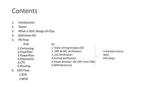
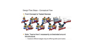
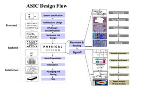
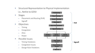
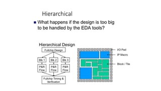
Module 3
Physical Design Flow
Contents
1. Introduction
2. Teams
3. What is ASIC Design of Chip
4. Definition PD
5. PD Flow
PnR
1.Partioning
2.FloorPlan
3.PowerPlan
4.Placement
5.CTS
6.Routing
6. ECO Flow
1.BTO
2.MTO
PV
1. Static timing Analysis (SI)
2. DRC & ERC Verification
3. LVS Verification
4.Formal Verification
5.Power Analysis (IR, EM, Cross Talk)
6.DFM (Antenna)
In Parallel chorus
With
PnR Steps
The Design
Teams
Physical Design
Verilog netlist
GDSII
SDC constraints
Front End
Team
Back End
Team
Fabrication
Team
ASIC Design Flow
Placement &
Routing
ENTITY test is
port a: in bit;
end ENTITY test;
LVS
ERC
Synthesize the
Design
RTL Design
and Verification
Mask Preparation
System Specification
Architectural Design
Chip
Packaging and
Testing
Floor Planning
Placement
Routing
Partitioning
CTS
P H Y S I C A L
Signoff
Static Timing Analysis
Formal Verification
Parasitic Extraction
Power Analysis
Physical Verification
Fabrication
F F F F F
F F F F F F
F F F F F
F F F F F F
F F F F F F
F
F
IR-Drop Analysis
Frontend
Backend
Fabrication
EDA Tools
EDA - electronic design automation.
• It is a software application that is used to develop electronic circuits.
• To ease the designing of integrated circuits on a large scale, companies use EDA tools.
Tools Required
• Innovus / ICC2 (for Floorplan to Route),
• Tempus / Prime Time (for Static Timing Analysis)
• PVS / Caliber (for Physical Verification like DRC, LVS)
• QRC / StarRC (for RC Extraction)
• Voltus / Redhawk (Power Analysis)
What is Physical Design?
• Physical Design of VLSI systems is the process of transforming structural representation (
gate-level netlist ) into layout representation.
• Structural representation : Is output of logic synthesis, that is performed using DC-
compiler or RTL-compiler.
• Layout representation : Is output of Place & Route Flow (P&R), which is in GDS-II format.
• Structural Representation to Physical Implementation
i.e., Netlist to GDSII
• Stages
— Placement and Routing (PnR)
— Signoff
• Objectives
— Timing
— Congestion
— Area
— Power
• Possible Issues
— Timing Violations
— Congestion Issues
— Design Rule Violations
Floor Planning
Placement
Signal Routing
Partitioning
Clock Tree Synthesis
Static Timing
Analysis
Formal
Verification
Parasitic
Extraction
Power, IR-Drop
Analysis
Physical
Verification
PnR
Signoff
Power Planning
Tape-out
Partitioning :
The process of decomposition of a larger system into smaller blocks is
called as “partitioning”.
20 million Gate
FULL-CHIP
5 million Gate
BLOCK-A
2.5 million Gate
BLOCK-B
2.5 million Gate
BLOCK-C
1.25 m Gate
BLOCK-D
1.25 m Gate
BLOCK-E
1.25 m Gate
BLOCK-G
1.25 m Gate
BLOCK-F
3.75 million Gate
BLOCK-H
1.25 m
Gate
BLOCK-I
Before Partitioning After Partitioning
 Smaller and manageable blocks are obtained.
 Easily handled by the tools and the available resources like
( CPU 's, memory).
 A partitioned module is called as soft block.
Hierarchical
 What happens if the design is too big
to be handled by the EDA tools?
Hierarchical Design
Fullchip Design I/O Pad
IP Macro
Blk 1 Blk 2 Blk 3
Block / Tile
P&R
Flow
P&R
Flow
P&R
Flow
Fullchip Timing &
Verification
Hierarchical
Design
 Hierarchical Design
Advantages
 Faster runtime, less memory needed for EDA tools
 Faster eco turn-around time
 Ability to do design re-use
Disadvantages
 Much more difficult for fullchip timing closure
(ILMs)
 More intensive design planning needed,
feedthrough generation, repeater insertion, timing
constraint budgeting.
Hierarchical Design
Partitions / Plan Groups
 Netlist must have partitions as top level modules.
 Partitions generally sized according to a target initial utilization
~70% utilization, ~300k-700k instances
 Channels or abutment
 Rectilinear block shapes are possible
Channels Abutment
Rectilinear
Blocks
Module 3.pptx

Module 3.pptx

  • 1.
  • 2.
    Contents 1. Introduction 2. Teams 3.What is ASIC Design of Chip 4. Definition PD 5. PD Flow PnR 1.Partioning 2.FloorPlan 3.PowerPlan 4.Placement 5.CTS 6.Routing 6. ECO Flow 1.BTO 2.MTO PV 1. Static timing Analysis (SI) 2. DRC & ERC Verification 3. LVS Verification 4.Formal Verification 5.Power Analysis (IR, EM, Cross Talk) 6.DFM (Antenna) In Parallel chorus With PnR Steps
  • 4.
    The Design Teams Physical Design Verilognetlist GDSII SDC constraints Front End Team Back End Team Fabrication Team
  • 5.
    ASIC Design Flow Placement& Routing ENTITY test is port a: in bit; end ENTITY test; LVS ERC Synthesize the Design RTL Design and Verification Mask Preparation System Specification Architectural Design Chip Packaging and Testing Floor Planning Placement Routing Partitioning CTS P H Y S I C A L Signoff Static Timing Analysis Formal Verification Parasitic Extraction Power Analysis Physical Verification Fabrication F F F F F F F F F F F F F F F F F F F F F F F F F F F F F F IR-Drop Analysis Frontend Backend Fabrication
  • 6.
    EDA Tools EDA -electronic design automation. • It is a software application that is used to develop electronic circuits. • To ease the designing of integrated circuits on a large scale, companies use EDA tools. Tools Required • Innovus / ICC2 (for Floorplan to Route), • Tempus / Prime Time (for Static Timing Analysis) • PVS / Caliber (for Physical Verification like DRC, LVS) • QRC / StarRC (for RC Extraction) • Voltus / Redhawk (Power Analysis)
  • 7.
    What is PhysicalDesign? • Physical Design of VLSI systems is the process of transforming structural representation ( gate-level netlist ) into layout representation. • Structural representation : Is output of logic synthesis, that is performed using DC- compiler or RTL-compiler. • Layout representation : Is output of Place & Route Flow (P&R), which is in GDS-II format.
  • 8.
    • Structural Representationto Physical Implementation i.e., Netlist to GDSII • Stages — Placement and Routing (PnR) — Signoff • Objectives — Timing — Congestion — Area — Power • Possible Issues — Timing Violations — Congestion Issues — Design Rule Violations Floor Planning Placement Signal Routing Partitioning Clock Tree Synthesis Static Timing Analysis Formal Verification Parasitic Extraction Power, IR-Drop Analysis Physical Verification PnR Signoff Power Planning Tape-out
  • 10.
    Partitioning : The processof decomposition of a larger system into smaller blocks is called as “partitioning”. 20 million Gate FULL-CHIP 5 million Gate BLOCK-A 2.5 million Gate BLOCK-B 2.5 million Gate BLOCK-C 1.25 m Gate BLOCK-D 1.25 m Gate BLOCK-E 1.25 m Gate BLOCK-G 1.25 m Gate BLOCK-F 3.75 million Gate BLOCK-H 1.25 m Gate BLOCK-I Before Partitioning After Partitioning  Smaller and manageable blocks are obtained.  Easily handled by the tools and the available resources like ( CPU 's, memory).  A partitioned module is called as soft block.
  • 11.
    Hierarchical  What happensif the design is too big to be handled by the EDA tools? Hierarchical Design Fullchip Design I/O Pad IP Macro Blk 1 Blk 2 Blk 3 Block / Tile P&R Flow P&R Flow P&R Flow Fullchip Timing & Verification
  • 12.
    Hierarchical Design  Hierarchical Design Advantages Faster runtime, less memory needed for EDA tools  Faster eco turn-around time  Ability to do design re-use Disadvantages  Much more difficult for fullchip timing closure (ILMs)  More intensive design planning needed, feedthrough generation, repeater insertion, timing constraint budgeting.
  • 13.
    Hierarchical Design Partitions /Plan Groups  Netlist must have partitions as top level modules.  Partitions generally sized according to a target initial utilization ~70% utilization, ~300k-700k instances  Channels or abutment  Rectilinear block shapes are possible Channels Abutment Rectilinear Blocks