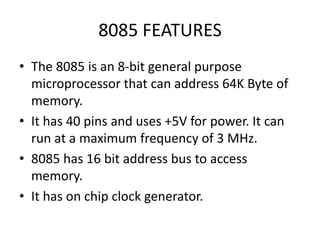
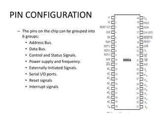
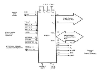
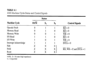
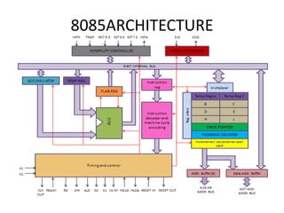
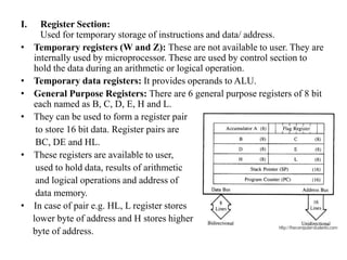
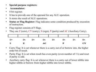
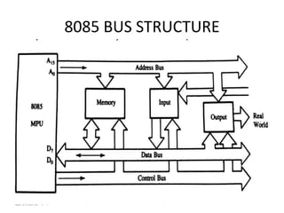
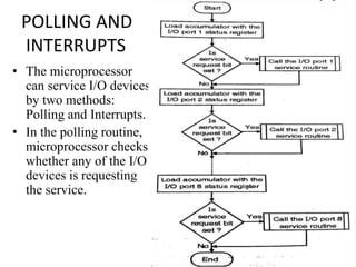
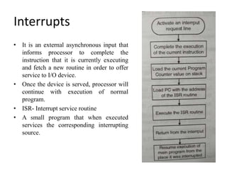
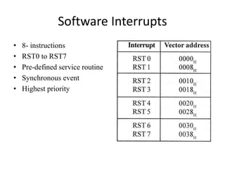
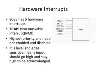
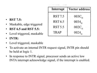
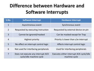
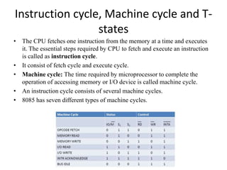
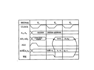
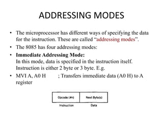
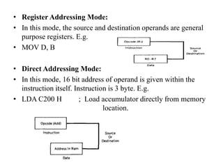
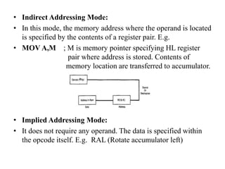
8085 MICROPROCESSOR
8085 FEATURES
• The 8085 is an 8-bit general purpose
microprocessor that can address 64K Byte of
memory.
• It has 40 pins and uses +5V for power. It can
run at a maximum frequency of 3 MHz.
• 8085 has 16 bit address bus to access
memory.
• It has on chip clock generator.
PIN CONFIGURATION
– The pins on the chip can be grouped into
6 groups:
• Address Bus.
• Data Bus.
• Control and Status Signals.
• Power supply and frequency.
• Externally Initiated Signals.
• Serial I/O ports.
• Reset signals
• Interrupt signals
• Power Supply signals: Vcc and Vss
• Vcc is to be connected to +5 V power supply
• Vss is ground reference
• Clock Signals: X1 and X2 and CLK OUT
• These are clock input signals, connected to crystal, LC or RC network.
• X1 and X2 pins drive internal clock generator circuit.
• The frequency is divided by 2 and used as operating frequency. Generally,
6.014 Mhz crystal is connected, this is divided by 2. so operating frequency
is 3.07 MHz.
• CLK OUT is an output signal used as system clock.
• This pin can be used by peripherals as a system clock input for their
operation.
• Reset Signals: RESET IN and RESET OUT
• RESET IN is an active low signal. When RESET IN = 0, it clears program
counter.
• RESET OUT is an active high signal used to indicate that microprocessor is
reset. It is used to reset other devices connected in system.
• Interrupt Signals: TRAP, RST 7.5, 6.5, 5.5, INTR,
INTA
Address bus and Data bus
• The address bus has 8 signal lines A8 – A15 which are unidirectional.
• The other 8 address bits are multiplexed (time shared) with the 8 data bits.
– So, the bits AD0 – AD7 are bi-directional and serve as A0 – A7 and D0
– D7 at the same time.
• During the execution of the instruction, these lines carry the
address bits during the early part, then during the late parts of the
execution, they carry the 8 data bits.
– In order to separate the address from the data, we can use a latch to
save the value before the function of the bits changes.
Status and Control Signals
• There are 4 main control and status signals. These are:
• ALE: Address Latch Enable. This signal is a pulse that become 1
when the AD0 – AD7 lines have an address on them. It becomes 0
after that. This signal can be used to enable a latch to save the
address bits from the AD lines.
• RD: Read. Active low- It is used to read data from selected
memory location or I/O location,
• WR: Write. Active low- It is used to write data to selected memory
location or I/O location.
• IO/M: This signal specifies whether the operation is a memory
operation (IO/M=0) or an I/O operation (IO/M=1).
• S1 and S0 : Status signals to specify the kind of operation being
performed.
• READY: It is used to detect whether a peripheral is ready for data
transfer or not.
•
8085ARCHITECTURE
I. Register Section:
Used for temporary storage of instructions and data/ address.
• Temporary registers (W and Z): These are not available to user. They are
internally used by microprocessor. These are used by control section to
hold the data during an arithmetic or logical operation.
• Temporary data registers: It provides operands to ALU.
• General Purpose Registers: There are 6 general purpose registers of 8 bit
each named as B, C, D, E, H and L.
• They can be used to form a register pair
to store 16 bit data. Register pairs are
BC, DE and HL.
• These registers are available to user,
used to hold data, results of arithmetic
and logical operations and address of
data memory.
• In case of pair e.g. HL, L register stores
lower byte of address and H stores higher
byte of address.
• Special purpose registers:
• Accumulator:
• 8 bit register.
• It has to provide one of the operand for any ALU operation.
• It stores the result of ALU operations.
• Status or Flag Register: Flag indicates some condition produced by execution
of instruction.
• Flag register consists of 5 flags.
• They are Z (zero), CY (carry), S (sign), P (parity) and AC (Auxiliary Carry).
• Carry Flag: It is set whenever there is a carry out of or borrow into, the higher
order bit of result.
• Parity Flag: It is set when result has even parity (even number of 1’s) and reset
if parity is odd.
• Auxiliary carry flag: It is set whenever there is a carry out of lower nibble into
higher nibble or borrow from higher nibble into lower nibble.
• Zero Flag: It is set if result of operation is zero.
• Sign Flag: It is set when MSB of the result is 1 (negative) and reset if MSB is 0
(positive).
• Instruction Register:
• It is not accessible to user.
• It holds the opcode of instruction that is decoded and executed. This opcode is
then further sent to instruction decoder to select one of the 256 operations.
• Program Counter (PC) : 16 bit
• Used to hold the address of program memory.
• It always points to the next instruction to be fetched i.e. it holds the memory
address of next instruction to be executed.
• Stack Pointer (SP) : 16 bit
• Stack is a reserved portion of memory where information can be stored or taken
back under software control. This area is called stack area.
• SP is used to define the stack starting address. It always point at top of the
stack.
• SP is decremented after each stack write operation and incremented after each
stack read operation.
II. Arithmetic and Logical Unit (ALU): 8 bit
• It performs arithmetic and logical operations.
• ALU is controlled by timing and control circuits.
• It accepts operands from accumulator and temporary register and stores the
result in accumulator.
• It provides status of result to flag register.
III. Instruction Decoder and Machine cycle Encoder:
• It accepts opcode from instruction register, decodes it and gives the decoded
information to control logic. It is a 8:256 decoder.
• The information includes what operation is to be performed, who will perform,
how many operand bytes the instruction contains.
• 8085 executes 7 types of machine cycles. The status signals give information
about which machine cycle is currently being executed.
IV. Address Buffer:
• 8 bit unidirectional buffer used for address lines.
• A buffer is used to isolate microprocessor from getting loaded due to high
current in other peripherals.
• These are used to drive higher order address bus.
V. Increment/ Decrement Address latch:
• 16 bit register used to increment or decrement address. Also used to latch the address.
VI. Interrupt Control:
• It accepts different interrupt request inputs.
• INTA is an acknowledgement pin for interrupt INTR.
• When a valid interrupt request is present it informs control logic to take action in
response to each signal.
• The processor has to be interrupted in order to service the interrupt. After completing
the interrupt service routine, returns back the control to main program.
VII. Serial I/O Control :
• For serial data transfer, SID and SOD signals are used.
• The data on these lines is accepted or transferred under software control by serial I/O
control block.
VIII. Timing and Control:
• It controls all internal and external circuits. It operates with reference to clock signal.
• It performs sequencing and synchronising operations. The synchronization is required
for communication between microprocessor and peripherals.
• It uses different status and control signals.
• Microprocessor uses quartz crystal to determine clock frequency .
8085 BUS STRUCTURE
• Address Bus
• Group of 16 lines (A0 to A15)
• Unidirectional : bits flow in one direction(from microprocessor to
peripheral)
• MPU is capable of addressing 2^16 =65,536 (64K)memory locations.
• Data Bus
• Group of 8 lines (D0 to D7)
• Bidirectional : data flow in both directions between microprocessor and
memory/ peripherals.
• Manipulate 8 bit data(00 to FF)(2^8=256 numbers)
• Control Bus:
• Comprised of various single lines that carry synchronization signals.
• MU generates specific control signals for every operation.
DEMULTIPLEXING ADDRESS AND DATA
BUS
• 74LS373 Latch is used to latch the address.
• ALE will go high to enable the latch. Output of latch is A7-A0.
• Before address disappears, ALE=0. The address will get
latched. Even input changes, output will not change.
• AD0-AD7 will now be used as data bus.
• Output of latch and upper order address in total provide 16 bit
address.
INSTRUCTION FETCHING AND
EXECUTION
• For fetching an instruction, 8085 places the contents of PC on A0 to A16
address lines, makes data bus available and activates a memory read control
signal.
• Instruction code is available on D0 to D7 lines.
• Microprocessor accepts contents of D0-D7 and transfers them to internal data
bus which is then accepted by instruction register and fetch operation is
complete.
• The OPCODE is then transferred to instruction decoder, it is decoded and
supplied to timing and control.
• Timing and control will perform the operation i.e. execution of instruction.
POLLING AND
INTERRUPTS
• The microprocessor
can service I/O devices
by two methods:
Polling and Interrupts.
• In the polling routine,
microprocessor checks
whether any of the I/O
devices is requesting
the service.
Interrupts
• It is an external asynchronous input that
informs processor to complete the
instruction that it is currently executing
and fetch a new routine in order to offer
service to I/O device.
• Once the device is served, processor will
continue with execution of normal
program.
• ISR- Interrupt service routine
• A small program that when executed
services the corresponding interrupting
source.
Types Of Interrupts
• Maskable interrupts are those which can be disable by the
programmer.
• That means, when disabled, even if the interrupt comes, the
MPU simply ignores it and doesn’t provide a service to it .
• Non maskable interrupt (NMI) is that which can’t be
disabled and when comes, MPU has to provide a service to it.
• Vectored interrupt: That transfer the program control to
specific memory locations.
• Non-vectored interrupt: The interrupted device should give
the address of the interrupt service routine (ISR).
• The software interrupts are program instructions. These
instructions are inserted at desired locations in a program.
• While running a program, if software interrupt instruction is
encountered, then the processor executes an interrupt service
routine (ISR).
• The hardware interrupts are initiated by an external device
by placing an appropriate signal at the interrupt pin of the
processor.
If the interrupt is accepted, then the processor executes an
interrupt service routine (ISR).
Software Interrupts
• 8- instructions
• RST0 to RST7
• Pre-defined service routine
• Synchronous event
• Highest priority
Hardware Interrupts
• 8085 has 5 hardware
interrupts:
• TRAP: Non maskable
interrupt(NMI).
• Highest priority and need
not enabled and disabled.
• It is level and edge
sensitive means input
should go high and stay
high to be acknowledged.
• RST 7.5:
• Maskable, edge triggered
• RST 6.5 and RST 5.5:
• Level triggered, maskable
• INTR:
• Level triggered, maskable
• To activate an internal INTR request signal, INTR pin should
be held at logic 1.
• In response to INTR signal, processor sends an active low
INTA interrupt acknowledge signal, if the interrupt is enabled.
Difference between Hardware and
Software Interrupts
S.No. Software Interrupt Hardware Interrupt
1 Asynchronous event Synchronous event
2 Requested by executing instruction Requested by external device on pin
3 Cannot be ignored/masked Can be masked except for Trap
4 Highest priority Priority is lower than s/w interrupt
5 No effect on interrupt control logic Affects interrupt control logic
6 Not used for interfacing peripherals Used for interfacing peripherals
7 Does not execute any interrupt ACK
cycle/idle machine cycle
Executes either interrupt ACK cycle/idle
machine cycle
INSTRUCTIONS
• An instruction is a binary pattern designed inside a microprocessor to
perform a specific function.
• The entire group of instructions, called the instruction set, determines
what functions the microprocessor can perform.
• Each instruction has two parts.
– The first part is the task or operation to be performed.
• This part is called the “opcode” (operation code).
– The second part is the data to be operated on
• Called the “operand”.
• The operand (or data) can be specified in various ways. It may include 8-bit
(or 16-bit ) data, an internal register, a memory location, or 8-bit (or 16-bit)
address.
Instruction word size
• The 8085 instruction set is classified into the
following three groups according to word size:
• 1. One-word or 1-byte instructions
• 2. Two-word or 2-byte instructions
• 3. Three-word or 3-byte instructions
One-Byte Instructions
• A 1-byte instruction includes the opcode and
operand in the same byte. Operand(s) are
internal register and are coded into the
instruction.
31
These instructions are stored in 8-bit binary format in memory; each requires
one memory location.
Two-Byte Instructions
• In a two-byte instruction, the first byte
specifies the operation code and the second
byte specifies the operand.
32
The instruction would require two memory locations to store in memory.
Three-Byte Instructions
• In a three-byte instruction, the first byte
specifies the opcode, and the following two
bytes specify the 16-bit address.
• Note that the second byte is the low-order
address and the third byte is the high-order
address.
• opcode + data byte + data byte
• This instruction would require three memory
locations to store in memory.
33
Instruction Set Classification
– These instructions can be grouped into five
different groups:
• Data Transfer Operations
• Arithmetic Operations
• Logic Operations
• Branch Operations
• Machine Control Operations
34
Data Transfer (Copy) Operations
• This group of instructions copy data from a
location called a source to another location
called a destination, without modifying the
contents of the source.
35
• Arithmetic Operations
• These instructions perform arithmetic
operations such as addition, subtraction,
increment, and decrement.
• Any 8-bit number, or the contents of a register
or the contents of a memory location can be
added to the contents of the accumulator and
the sum is stored in the accumulator.
• No two other 8-bit registers can be added
directly (e.g., the contents of register B cannot
be added directly to the contents of the register
C).
36
Logical Operations
• These instructions perform various logical
operations with the contents of the
accumulator.
• AND, OR Exclusive-OR
• Rotate
• Compare
• Complement
37
Branching Operations
• This group of instructions alters the sequence of
program execution.
• Jump-These instructions test for a certain
conditions and alter the program sequence when
the condition is met.
• Call, Return, and Restart - These instructions
change the sequence of a program either by
calling a subroutine or returning from a
subroutine.
• The conditional Call and Return instructions also
can test condition flags.
38
Machine Control Operations
• These instructions control machine functions
such as
• Halt,
• Interrupt, or do nothing.
39
Instruction cycle, Machine cycle and T-
states
• The CPU fetches one instruction from the memory at a time and executes
it. The essential steps required by CPU to fetch and execute an instruction
is called as instruction cycle.
• It consist of fetch cycle and execute cycle.
• Machine cycle: The time required by microprocessor to complete the
operation of accessing memory or I/O device is called machine cycle.
• An instruction cycle consists of several machine cycles.
• 8085 has seven different types of machine cycles.
T states
• Microprocessor perform an operation in a specific time period i.e. specific
clock cycle. Each clock cycle is called as T-state.
• The number of T states required to perform an operation is called as
machine cycle.
• Machine cycle consists of 3 to 6 T states.
• An instruction cycle consists of 1 to 5 machine cycles.
OPCODE FETCH CYCLE
• The first step of executing any instruction is the Opcode fetch cycle.
– In this cycle, the microprocessor brings in the instruction’s Opcode
from memory.
• To differentiate this machine cycle from the very similar “memory
read” cycle, the control & status signals are set as follows:
– IO/M=0, s0 and s1 are both 1.
– This machine cycle has four T-states.
• The 8085 uses the first 3 T-states to fetch the opcode.
• T4 is used to decode and execute it.
– It is also possible for an instruction to have 6 T-states in an opcode
fetch machine cycle.
OPERAND FETCH OR MEMORY READ
CYCLE
• The memory read machine cycle is exactly the same as the opcode fetch
except:
– It only has 3 T-states
– The s0 signal is set to 0 instead.
MEMORY WRITE CYCLE
• To store data either in data memory or stack
memory.
– The 8085 places the address (2065H) on the
address bus
– Identifies the operation as a memory write
(IO/M=0, s1=0, s0=1).
– Places the contents of the accumulator on the
data bus and asserts the signal WR.
– During the last T-state, the contents of the data
bus are saved into the memory location.
ADDRESSING MODES
• The microprocessor has different ways of specifying the data
for the instruction. These are called “addressing modes”.
• The 8085 has four addressing modes:
• Immediate Addressing Mode:
In this mode, data is specified in the instruction itself.
Instruction is either 2 byte or 3 byte. E.g.
• MVI A, A0 H ; Transfers immediate data (A0 H) to A
register
• Register Addressing Mode:
• In this mode, the source and destination operands are general
purpose registers. E.g.
• MOV D, B
• Direct Addressing Mode:
• In this mode, 16 bit address of operand is given within the
instruction itself. Instruction is 3 byte. E.g.
• LDA C200 H ; Load accumulator directly from memory
location.
• Indirect Addressing Mode:
• In this mode, the memory address where the operand is located
is specified by the contents of a register pair. E.g.
• MOV A,M ; M is memory pointer specifying HL register
pair where address is stored. Contents of
memory location are transferred to accumulator.
• Implied Addressing Mode:
• It does not require any operand. The data is specified within
the opcode itself. E.g. RAL (Rotate accumulator left)

8085 microprocessor

  • 1.
  • 2.
    8085 FEATURES • The8085 is an 8-bit general purpose microprocessor that can address 64K Byte of memory. • It has 40 pins and uses +5V for power. It can run at a maximum frequency of 3 MHz. • 8085 has 16 bit address bus to access memory. • It has on chip clock generator.
  • 3.
    PIN CONFIGURATION – Thepins on the chip can be grouped into 6 groups: • Address Bus. • Data Bus. • Control and Status Signals. • Power supply and frequency. • Externally Initiated Signals. • Serial I/O ports. • Reset signals • Interrupt signals
  • 5.
    • Power Supplysignals: Vcc and Vss • Vcc is to be connected to +5 V power supply • Vss is ground reference • Clock Signals: X1 and X2 and CLK OUT • These are clock input signals, connected to crystal, LC or RC network. • X1 and X2 pins drive internal clock generator circuit. • The frequency is divided by 2 and used as operating frequency. Generally, 6.014 Mhz crystal is connected, this is divided by 2. so operating frequency is 3.07 MHz. • CLK OUT is an output signal used as system clock. • This pin can be used by peripherals as a system clock input for their operation. • Reset Signals: RESET IN and RESET OUT • RESET IN is an active low signal. When RESET IN = 0, it clears program counter. • RESET OUT is an active high signal used to indicate that microprocessor is reset. It is used to reset other devices connected in system.
  • 6.
    • Interrupt Signals:TRAP, RST 7.5, 6.5, 5.5, INTR, INTA
  • 7.
    Address bus andData bus • The address bus has 8 signal lines A8 – A15 which are unidirectional. • The other 8 address bits are multiplexed (time shared) with the 8 data bits. – So, the bits AD0 – AD7 are bi-directional and serve as A0 – A7 and D0 – D7 at the same time. • During the execution of the instruction, these lines carry the address bits during the early part, then during the late parts of the execution, they carry the 8 data bits. – In order to separate the address from the data, we can use a latch to save the value before the function of the bits changes.
  • 8.
    Status and ControlSignals • There are 4 main control and status signals. These are: • ALE: Address Latch Enable. This signal is a pulse that become 1 when the AD0 – AD7 lines have an address on them. It becomes 0 after that. This signal can be used to enable a latch to save the address bits from the AD lines. • RD: Read. Active low- It is used to read data from selected memory location or I/O location, • WR: Write. Active low- It is used to write data to selected memory location or I/O location. • IO/M: This signal specifies whether the operation is a memory operation (IO/M=0) or an I/O operation (IO/M=1). • S1 and S0 : Status signals to specify the kind of operation being performed. • READY: It is used to detect whether a peripheral is ready for data transfer or not.
  • 10.
  • 11.
    I. Register Section: Usedfor temporary storage of instructions and data/ address. • Temporary registers (W and Z): These are not available to user. They are internally used by microprocessor. These are used by control section to hold the data during an arithmetic or logical operation. • Temporary data registers: It provides operands to ALU. • General Purpose Registers: There are 6 general purpose registers of 8 bit each named as B, C, D, E, H and L. • They can be used to form a register pair to store 16 bit data. Register pairs are BC, DE and HL. • These registers are available to user, used to hold data, results of arithmetic and logical operations and address of data memory. • In case of pair e.g. HL, L register stores lower byte of address and H stores higher byte of address.
  • 12.
    • Special purposeregisters: • Accumulator: • 8 bit register. • It has to provide one of the operand for any ALU operation. • It stores the result of ALU operations. • Status or Flag Register: Flag indicates some condition produced by execution of instruction. • Flag register consists of 5 flags. • They are Z (zero), CY (carry), S (sign), P (parity) and AC (Auxiliary Carry). • Carry Flag: It is set whenever there is a carry out of or borrow into, the higher order bit of result. • Parity Flag: It is set when result has even parity (even number of 1’s) and reset if parity is odd. • Auxiliary carry flag: It is set whenever there is a carry out of lower nibble into higher nibble or borrow from higher nibble into lower nibble.
  • 13.
    • Zero Flag:It is set if result of operation is zero. • Sign Flag: It is set when MSB of the result is 1 (negative) and reset if MSB is 0 (positive). • Instruction Register: • It is not accessible to user. • It holds the opcode of instruction that is decoded and executed. This opcode is then further sent to instruction decoder to select one of the 256 operations. • Program Counter (PC) : 16 bit • Used to hold the address of program memory. • It always points to the next instruction to be fetched i.e. it holds the memory address of next instruction to be executed. • Stack Pointer (SP) : 16 bit • Stack is a reserved portion of memory where information can be stored or taken back under software control. This area is called stack area. • SP is used to define the stack starting address. It always point at top of the stack. • SP is decremented after each stack write operation and incremented after each stack read operation.
  • 14.
    II. Arithmetic andLogical Unit (ALU): 8 bit • It performs arithmetic and logical operations. • ALU is controlled by timing and control circuits. • It accepts operands from accumulator and temporary register and stores the result in accumulator. • It provides status of result to flag register. III. Instruction Decoder and Machine cycle Encoder: • It accepts opcode from instruction register, decodes it and gives the decoded information to control logic. It is a 8:256 decoder. • The information includes what operation is to be performed, who will perform, how many operand bytes the instruction contains. • 8085 executes 7 types of machine cycles. The status signals give information about which machine cycle is currently being executed. IV. Address Buffer: • 8 bit unidirectional buffer used for address lines. • A buffer is used to isolate microprocessor from getting loaded due to high current in other peripherals. • These are used to drive higher order address bus.
  • 15.
    V. Increment/ DecrementAddress latch: • 16 bit register used to increment or decrement address. Also used to latch the address. VI. Interrupt Control: • It accepts different interrupt request inputs. • INTA is an acknowledgement pin for interrupt INTR. • When a valid interrupt request is present it informs control logic to take action in response to each signal. • The processor has to be interrupted in order to service the interrupt. After completing the interrupt service routine, returns back the control to main program. VII. Serial I/O Control : • For serial data transfer, SID and SOD signals are used. • The data on these lines is accepted or transferred under software control by serial I/O control block. VIII. Timing and Control: • It controls all internal and external circuits. It operates with reference to clock signal. • It performs sequencing and synchronising operations. The synchronization is required for communication between microprocessor and peripherals. • It uses different status and control signals. • Microprocessor uses quartz crystal to determine clock frequency .
  • 16.
  • 17.
    • Address Bus •Group of 16 lines (A0 to A15) • Unidirectional : bits flow in one direction(from microprocessor to peripheral) • MPU is capable of addressing 2^16 =65,536 (64K)memory locations. • Data Bus • Group of 8 lines (D0 to D7) • Bidirectional : data flow in both directions between microprocessor and memory/ peripherals. • Manipulate 8 bit data(00 to FF)(2^8=256 numbers) • Control Bus: • Comprised of various single lines that carry synchronization signals. • MU generates specific control signals for every operation.
  • 18.
    DEMULTIPLEXING ADDRESS ANDDATA BUS • 74LS373 Latch is used to latch the address. • ALE will go high to enable the latch. Output of latch is A7-A0. • Before address disappears, ALE=0. The address will get latched. Even input changes, output will not change. • AD0-AD7 will now be used as data bus. • Output of latch and upper order address in total provide 16 bit address.
  • 20.
    INSTRUCTION FETCHING AND EXECUTION •For fetching an instruction, 8085 places the contents of PC on A0 to A16 address lines, makes data bus available and activates a memory read control signal. • Instruction code is available on D0 to D7 lines. • Microprocessor accepts contents of D0-D7 and transfers them to internal data bus which is then accepted by instruction register and fetch operation is complete. • The OPCODE is then transferred to instruction decoder, it is decoded and supplied to timing and control. • Timing and control will perform the operation i.e. execution of instruction.
  • 21.
    POLLING AND INTERRUPTS • Themicroprocessor can service I/O devices by two methods: Polling and Interrupts. • In the polling routine, microprocessor checks whether any of the I/O devices is requesting the service.
  • 22.
    Interrupts • It isan external asynchronous input that informs processor to complete the instruction that it is currently executing and fetch a new routine in order to offer service to I/O device. • Once the device is served, processor will continue with execution of normal program. • ISR- Interrupt service routine • A small program that when executed services the corresponding interrupting source.
  • 23.
    Types Of Interrupts •Maskable interrupts are those which can be disable by the programmer. • That means, when disabled, even if the interrupt comes, the MPU simply ignores it and doesn’t provide a service to it . • Non maskable interrupt (NMI) is that which can’t be disabled and when comes, MPU has to provide a service to it. • Vectored interrupt: That transfer the program control to specific memory locations. • Non-vectored interrupt: The interrupted device should give the address of the interrupt service routine (ISR).
  • 24.
    • The softwareinterrupts are program instructions. These instructions are inserted at desired locations in a program. • While running a program, if software interrupt instruction is encountered, then the processor executes an interrupt service routine (ISR). • The hardware interrupts are initiated by an external device by placing an appropriate signal at the interrupt pin of the processor. If the interrupt is accepted, then the processor executes an interrupt service routine (ISR).
  • 25.
    Software Interrupts • 8-instructions • RST0 to RST7 • Pre-defined service routine • Synchronous event • Highest priority
  • 26.
    Hardware Interrupts • 8085has 5 hardware interrupts: • TRAP: Non maskable interrupt(NMI). • Highest priority and need not enabled and disabled. • It is level and edge sensitive means input should go high and stay high to be acknowledged.
  • 27.
    • RST 7.5: •Maskable, edge triggered • RST 6.5 and RST 5.5: • Level triggered, maskable • INTR: • Level triggered, maskable • To activate an internal INTR request signal, INTR pin should be held at logic 1. • In response to INTR signal, processor sends an active low INTA interrupt acknowledge signal, if the interrupt is enabled.
  • 28.
    Difference between Hardwareand Software Interrupts S.No. Software Interrupt Hardware Interrupt 1 Asynchronous event Synchronous event 2 Requested by executing instruction Requested by external device on pin 3 Cannot be ignored/masked Can be masked except for Trap 4 Highest priority Priority is lower than s/w interrupt 5 No effect on interrupt control logic Affects interrupt control logic 6 Not used for interfacing peripherals Used for interfacing peripherals 7 Does not execute any interrupt ACK cycle/idle machine cycle Executes either interrupt ACK cycle/idle machine cycle
  • 29.
    INSTRUCTIONS • An instructionis a binary pattern designed inside a microprocessor to perform a specific function. • The entire group of instructions, called the instruction set, determines what functions the microprocessor can perform. • Each instruction has two parts. – The first part is the task or operation to be performed. • This part is called the “opcode” (operation code). – The second part is the data to be operated on • Called the “operand”. • The operand (or data) can be specified in various ways. It may include 8-bit (or 16-bit ) data, an internal register, a memory location, or 8-bit (or 16-bit) address.
  • 30.
    Instruction word size •The 8085 instruction set is classified into the following three groups according to word size: • 1. One-word or 1-byte instructions • 2. Two-word or 2-byte instructions • 3. Three-word or 3-byte instructions
  • 31.
    One-Byte Instructions • A1-byte instruction includes the opcode and operand in the same byte. Operand(s) are internal register and are coded into the instruction. 31 These instructions are stored in 8-bit binary format in memory; each requires one memory location.
  • 32.
    Two-Byte Instructions • Ina two-byte instruction, the first byte specifies the operation code and the second byte specifies the operand. 32 The instruction would require two memory locations to store in memory.
  • 33.
    Three-Byte Instructions • Ina three-byte instruction, the first byte specifies the opcode, and the following two bytes specify the 16-bit address. • Note that the second byte is the low-order address and the third byte is the high-order address. • opcode + data byte + data byte • This instruction would require three memory locations to store in memory. 33
  • 34.
    Instruction Set Classification –These instructions can be grouped into five different groups: • Data Transfer Operations • Arithmetic Operations • Logic Operations • Branch Operations • Machine Control Operations 34
  • 35.
    Data Transfer (Copy)Operations • This group of instructions copy data from a location called a source to another location called a destination, without modifying the contents of the source. 35
  • 36.
    • Arithmetic Operations •These instructions perform arithmetic operations such as addition, subtraction, increment, and decrement. • Any 8-bit number, or the contents of a register or the contents of a memory location can be added to the contents of the accumulator and the sum is stored in the accumulator. • No two other 8-bit registers can be added directly (e.g., the contents of register B cannot be added directly to the contents of the register C). 36
  • 37.
    Logical Operations • Theseinstructions perform various logical operations with the contents of the accumulator. • AND, OR Exclusive-OR • Rotate • Compare • Complement 37
  • 38.
    Branching Operations • Thisgroup of instructions alters the sequence of program execution. • Jump-These instructions test for a certain conditions and alter the program sequence when the condition is met. • Call, Return, and Restart - These instructions change the sequence of a program either by calling a subroutine or returning from a subroutine. • The conditional Call and Return instructions also can test condition flags. 38
  • 39.
    Machine Control Operations •These instructions control machine functions such as • Halt, • Interrupt, or do nothing. 39
  • 40.
    Instruction cycle, Machinecycle and T- states • The CPU fetches one instruction from the memory at a time and executes it. The essential steps required by CPU to fetch and execute an instruction is called as instruction cycle. • It consist of fetch cycle and execute cycle. • Machine cycle: The time required by microprocessor to complete the operation of accessing memory or I/O device is called machine cycle. • An instruction cycle consists of several machine cycles. • 8085 has seven different types of machine cycles.
  • 41.
    T states • Microprocessorperform an operation in a specific time period i.e. specific clock cycle. Each clock cycle is called as T-state. • The number of T states required to perform an operation is called as machine cycle. • Machine cycle consists of 3 to 6 T states. • An instruction cycle consists of 1 to 5 machine cycles.
  • 42.
    OPCODE FETCH CYCLE •The first step of executing any instruction is the Opcode fetch cycle. – In this cycle, the microprocessor brings in the instruction’s Opcode from memory. • To differentiate this machine cycle from the very similar “memory read” cycle, the control & status signals are set as follows: – IO/M=0, s0 and s1 are both 1. – This machine cycle has four T-states. • The 8085 uses the first 3 T-states to fetch the opcode. • T4 is used to decode and execute it. – It is also possible for an instruction to have 6 T-states in an opcode fetch machine cycle.
  • 44.
    OPERAND FETCH ORMEMORY READ CYCLE • The memory read machine cycle is exactly the same as the opcode fetch except: – It only has 3 T-states – The s0 signal is set to 0 instead.
  • 45.
    MEMORY WRITE CYCLE •To store data either in data memory or stack memory. – The 8085 places the address (2065H) on the address bus – Identifies the operation as a memory write (IO/M=0, s1=0, s0=1). – Places the contents of the accumulator on the data bus and asserts the signal WR. – During the last T-state, the contents of the data bus are saved into the memory location.
  • 47.
    ADDRESSING MODES • Themicroprocessor has different ways of specifying the data for the instruction. These are called “addressing modes”. • The 8085 has four addressing modes: • Immediate Addressing Mode: In this mode, data is specified in the instruction itself. Instruction is either 2 byte or 3 byte. E.g. • MVI A, A0 H ; Transfers immediate data (A0 H) to A register
  • 48.
    • Register AddressingMode: • In this mode, the source and destination operands are general purpose registers. E.g. • MOV D, B • Direct Addressing Mode: • In this mode, 16 bit address of operand is given within the instruction itself. Instruction is 3 byte. E.g. • LDA C200 H ; Load accumulator directly from memory location.
  • 49.
    • Indirect AddressingMode: • In this mode, the memory address where the operand is located is specified by the contents of a register pair. E.g. • MOV A,M ; M is memory pointer specifying HL register pair where address is stored. Contents of memory location are transferred to accumulator. • Implied Addressing Mode: • It does not require any operand. The data is specified within the opcode itself. E.g. RAL (Rotate accumulator left)