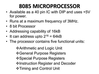
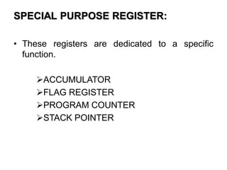
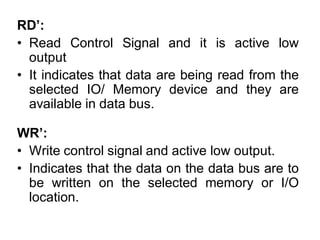
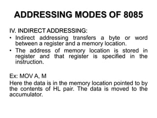
The document discusses the 8085 microprocessor. It contains details about its architecture, registers, buses, instructions and interrupts. The 8085 is an 8-bit microprocessor available as a 40-pin IC that runs at 3MHz maximum frequency. It has five functional units: ALU, general purpose registers, special purpose registers, instruction register and decoder, and timing and control unit. The document describes each of these units and their roles in the 8085 architecture.
MICROPROCESSOR AND INTERFACING
8255A : ppi
8259A : pic
Basics of 8255A PPI
Different I/O mode of 8255A
Basics of 8259A PIC
Different interrupt mode of 8259A
Programming Mode of 8259A
In this session you will learn:
Programmable Logic Controller(PLC)
Types of PLC’s
PLC architecture
Scan cycles
Scan patterns
PLC programming
Ladder diagram programming
Latch and Unlatch
DCS architecture
For more information, visit: https://www.mindsmapped.com/courses/industrial-automation/complete-training-on-industrial-automation-for-beginners/
8085 Microprocessor Architecture for beginners.It explains the Instruction Register(IR),Instruction Decoder, Address buffer register,Address data buffer,program execution,Serial I/O control etc.
Hybrid optimization of pumped hydro system and solar- Engr. Abdul-Azeez.pdffxintegritypublishin
Advancements in technology unveil a myriad of electrical and electronic breakthroughs geared towards efficiently harnessing limited resources to meet human energy demands. The optimization of hybrid solar PV panels and pumped hydro energy supply systems plays a pivotal role in utilizing natural resources effectively. This initiative not only benefits humanity but also fosters environmental sustainability. The study investigated the design optimization of these hybrid systems, focusing on understanding solar radiation patterns, identifying geographical influences on solar radiation, formulating a mathematical model for system optimization, and determining the optimal configuration of PV panels and pumped hydro storage. Through a comparative analysis approach and eight weeks of data collection, the study addressed key research questions related to solar radiation patterns and optimal system design. The findings highlighted regions with heightened solar radiation levels, showcasing substantial potential for power generation and emphasizing the system's efficiency. Optimizing system design significantly boosted power generation, promoted renewable energy utilization, and enhanced energy storage capacity. The study underscored the benefits of optimizing hybrid solar PV panels and pumped hydro energy supply systems for sustainable energy usage. Optimizing the design of solar PV panels and pumped hydro energy supply systems as examined across diverse climatic conditions in a developing country, not only enhances power generation but also improves the integration of renewable energy sources and boosts energy storage capacities, particularly beneficial for less economically prosperous regions. Additionally, the study provides valuable insights for advancing energy research in economically viable areas. Recommendations included conducting site-specific assessments, utilizing advanced modeling tools, implementing regular maintenance protocols, and enhancing communication among system components.
Immunizing Image Classifiers Against Localized Adversary Attacksgerogepatton
This paper addresses the vulnerability of deep learning models, particularly convolutional neural networks
(CNN)s, to adversarial attacks and presents a proactive training technique designed to counter them. We
introduce a novel volumization algorithm, which transforms 2D images into 3D volumetric representations.
When combined with 3D convolution and deep curriculum learning optimization (CLO), itsignificantly improves
the immunity of models against localized universal attacks by up to 40%. We evaluate our proposed approach
using contemporary CNN architectures and the modified Canadian Institute for Advanced Research (CIFAR-10
and CIFAR-100) and ImageNet Large Scale Visual Recognition Challenge (ILSVRC12) datasets, showcasing
accuracy improvements over previous techniques. The results indicate that the combination of the volumetric
input and curriculum learning holds significant promise for mitigating adversarial attacks without necessitating
adversary training.
Welcome to WIPAC Monthly the magazine brought to you by the LinkedIn Group Water Industry Process Automation & Control.
In this month's edition, along with this month's industry news to celebrate the 13 years since the group was created we have articles including
A case study of the used of Advanced Process Control at the Wastewater Treatment works at Lleida in Spain
A look back on an article on smart wastewater networks in order to see how the industry has measured up in the interim around the adoption of Digital Transformation in the Water Industry.
Water scarcity is the lack of fresh water resources to meet the standard water demand. There are two type of water scarcity. One is physical. The other is economic water scarcity.
Cosmetic shop management system project report.pdfKamal Acharya
Buying new cosmetic products is difficult. It can even be scary for those who have sensitive skin and are prone to skin trouble. The information needed to alleviate this problem is on the back of each product, but it's thought to interpret those ingredient lists unless you have a background in chemistry.
Instead of buying and hoping for the best, we can use data science to help us predict which products may be good fits for us. It includes various function programs to do the above mentioned tasks.
Data file handling has been effectively used in the program.
The automated cosmetic shop management system should deal with the automation of general workflow and administration process of the shop. The main processes of the system focus on customer's request where the system is able to search the most appropriate products and deliver it to the customers. It should help the employees to quickly identify the list of cosmetic product that have reached the minimum quantity and also keep a track of expired date for each cosmetic product. It should help the employees to find the rack number in which the product is placed.It is also Faster and more efficient way.
About
Indigenized remote control interface card suitable for MAFI system CCR equipment. Compatible for IDM8000 CCR. Backplane mounted serial and TCP/Ethernet communication module for CCR remote access. IDM 8000 CCR remote control on serial and TCP protocol.
• Remote control: Parallel or serial interface.
• Compatible with MAFI CCR system.
• Compatible with IDM8000 CCR.
• Compatible with Backplane mount serial communication.
• Compatible with commercial and Defence aviation CCR system.
• Remote control system for accessing CCR and allied system over serial or TCP.
• Indigenized local Support/presence in India.
• Easy in configuration using DIP switches.
Technical Specifications
Indigenized remote control interface card suitable for MAFI system CCR equipment. Compatible for IDM8000 CCR. Backplane mounted serial and TCP/Ethernet communication module for CCR remote access. IDM 8000 CCR remote control on serial and TCP protocol.
Key Features
Indigenized remote control interface card suitable for MAFI system CCR equipment. Compatible for IDM8000 CCR. Backplane mounted serial and TCP/Ethernet communication module for CCR remote access. IDM 8000 CCR remote control on serial and TCP protocol.
• Remote control: Parallel or serial interface
• Compatible with MAFI CCR system
• Copatiable with IDM8000 CCR
• Compatible with Backplane mount serial communication.
• Compatible with commercial and Defence aviation CCR system.
• Remote control system for accessing CCR and allied system over serial or TCP.
• Indigenized local Support/presence in India.
Application
• Remote control: Parallel or serial interface.
• Compatible with MAFI CCR system.
• Compatible with IDM8000 CCR.
• Compatible with Backplane mount serial communication.
• Compatible with commercial and Defence aviation CCR system.
• Remote control system for accessing CCR and allied system over serial or TCP.
• Indigenized local Support/presence in India.
• Easy in configuration using DIP switches.
Explore the innovative world of trenchless pipe repair with our comprehensive guide, "The Benefits and Techniques of Trenchless Pipe Repair." This document delves into the modern methods of repairing underground pipes without the need for extensive excavation, highlighting the numerous advantages and the latest techniques used in the industry.
Learn about the cost savings, reduced environmental impact, and minimal disruption associated with trenchless technology. Discover detailed explanations of popular techniques such as pipe bursting, cured-in-place pipe (CIPP) lining, and directional drilling. Understand how these methods can be applied to various types of infrastructure, from residential plumbing to large-scale municipal systems.
Ideal for homeowners, contractors, engineers, and anyone interested in modern plumbing solutions, this guide provides valuable insights into why trenchless pipe repair is becoming the preferred choice for pipe rehabilitation. Stay informed about the latest advancements and best practices in the field.
Student information management system project report ii.pdfKamal Acharya
Our project explains about the student management. This project mainly explains the various actions related to student details. This project shows some ease in adding, editing and deleting the student details. It also provides a less time consuming process for viewing, adding, editing and deleting the marks of the students.
Student information management system project report ii.pdf
MPMC
1. 8085 MICROPROCESSOR
Ms. J. Glory Priyadharshini,
Assistant Professor/EEE,
Sri Ramakrishna Institute of Technology
2. 8085 MICROPROCESSOR
• Available as a 40 pin IC with DIP and uses +5V
for power.
• Runs at a maximum frequency of 3MHz.
• 8 bit Processor
• Addressing capability of 16kB
• It can address upto 216 = 64kB
• The processor contains five functional units:
Arithmetic and Logic Unit
General Purpose Registers
Special Purpose Registers
Instruction Register and Decoder
Timing and Control Unit
5. ARITHMETIC & LOGIC UNIT
• It performs various arithmetic & logic operations.
• Possible arithmetic operations are addition (ADD),
subtraction (SUB), increment (INR), decrement
(DCR) and comparision (CMP).
• Possible logical operations are AND, OR, EXOR etc.
• The ALU of the processor is called accumulator
oriented ALU as one of the operand used arithmetic
& logic operation must be stored in Accumulator.
• The other data is taken from a memory location or
register.
• The result of the arithmetic and logical operations is
stored in accumulator.
6. GENERAL PURPOSE REGISTER
• It is used to store data that is being used by the
program under execution.
• The 8085 has six general-purpose registers to
store 8-bit data, they are B, C, D, E, H and L.
• They are also called as scratch pad registers.
• In almost all arithmetic & logic operations, these
registers are used to store the second operand.
• They can also be handled as 16 bit register pairs
by combining BC, DE and HL to perform some
16-bit operations.
• Among these pairs HL pair is used as memory
pointer in few memory related instructions
7. SPECIAL PURPOSE REGISTER:
• These registers are dedicated to a specific
function.
ACCUMULATOR
FLAG REGISTER
PROGRAM COUNTER
STACK POINTER
8. Accumulator:
• Is an 8 bit register
• It is also called as A register
• It is a part of arithmetic & logic unit
• It always contains 1 of the operands on
which arithmetic & logic operations has to
be performed.
• After arithmetic/logic operation the
contents of the accumulator are replaced
by the result.
9. Flag Register:
• The flag is an 8 bit register used to indicate the
Status of recent arithmetic or logical operation.
S=sign, z=zero, AC=auxiliary carry, p=parity,
CY=carry
10. Zero flag:
• Result stored in accumulator is zero or not after the operation
is performed.
• Result- zero, flag is set.
• Result- not zero, flag is reset.
Auxiliary carry flag:
• It is also called as half carry
• This carry is generated when a carry results from bit D3 and
passes on to D4 i.e., from lower nibble to higher nibble
• It may also occur in subtraction operation i.e., it is set when
borrow is generated.
• It cannot be accessed externally.
11. Sign flag:
• It is just a Copy of the bit D7 in Accumulator(MSB)
• result –ve, flag is set ‘1’ i.e., D7=1
• result +ve, flag is reset ‘0’ i.e., D7=0
• Indicates sign of a number and used in signed arithmetic
operation.
Parity flag:
• This flag is set when content of accumulator has even
number of 1s.
• i.e., Parity is even, parity flag is set; Parity is odd, parity
flag is reset.
Carry Flag:
• Carry flag is set when an extra bit is generated in the
process of arithmetic operation. i.e., extra bit from D7
12. Program Counter:
• It is used to hold the address of next instruction to be
executed.
• It is a 16 bit register
Stack pointer:
• Stack is an array of memory locations organized in LIFO
fashion. It accessed using a 16 bit pointer register called
SP.
• It holds the address of the top most element in the stack
• It is 16 bit register.
• Any part of memory can be used as stack.
• Stack is used to store the return address of the main
program when a subroutine is called.
13. INSTRUCTION REGISTER AND DECODER
Instruction Register:
• It is used to hold the current instruction which the
microprocessor is about to execute.
• It is an 8 bit register.
• In addition there are two temporary registers W and
Z which are controlled internally and not available or
user access.
Instruction decoder:
• The content of the instruction register is decoded by
the decoder circuitry.
• It generates various machine cycle depending upon
the instruction.
• The machine cycles are then given to timing and
control unit.
14. TIMING AND CONTROL UNIT
• It control all the operation of microprocessor and
peripheral devices.
• The timing and control unit gets commands from
the instruction decoder and issues signals on the
data bus, address bus and control bus.
Bus:
• The microprocessor performs its functions using
wires or lines called buses.
• A typical microprocessor communicates with
memory and input/output devices using buses.
• There are three types of buses – the address bus,
the data bus and the control bus.
15. Data Bus:
• Data bus is two way bus carrying data around the
system.
• It carries data in binary form between
microprocessor, memory and peripherals.
• The data bus width of 8085 microprocessor is 8-bit.
• The lower group of eight address lines A0-A7 is
multiplexed with the data bus in order to reduce the
pin count.
16. Address Bus:
• The address bus carries addresses and is one way
bus from the microprocessor to memory or other
devices.
• It is group of sixteen unidirectional lines that allows
flow of address from the processor to its peripheral
devices.
• Address lines are identified as A0-A15 of which the
higher order address lines i.e., A8-A15 are
unidirectional and lower order lines A0-A7 are
multiplexed with data lines D0-D7, hence
bidirectional.
• To separate the address from data, address latch
enable(ALE) is used.
17. Control Bus:
• Control bus are various lines which have specific
functions for coordinating and controlling
microprocessor operations.
• The control bus carries control signals that are
partly unidirectional and partly bidirectional.
Control Signals: READY, RD’, WR’, ALE
Status Signals: S0, S1, IO/M’
DMA Signals: HOLD, HLDA
RESET Signals: RESET IN, RESET OUT
18. ALE:
• Address Latch Enable
• During the first clock state of a machine cycle, it
becomes high and enables address to get
latched i.e., ALE=1, address/data latch contains
lower byte of address, ALE=0, it contains 8 bit
data.
IO/M’:
It is signal that distinguishes between a memory
and an I/O operation.
IO/M’=0 Memory Operation
IO/M’=1 I/O operation
19. RD’:
• Read Control Signal and it is active low
output
• It indicates that data are being read from the
selected IO/ Memory device and they are
available in data bus.
WR’:
• Write control signal and active low output.
• Indicates that the data on the data bus are to
be written on the selected memory or I/O
location.
20. S1 and S0:
• These are status signals sent by the
microprocessor to distinguish the various types
of operation being performed.
• These signals combine with IO/M’
signals to govern various operations.
21. READY :
• This pin is used to synchronise slower peripheral
devices with fast microprocessor.
• A low value causes the microprocessor to enter
into wait state.
• The microprocessor remains in wait state until
the input at this pin goes high.
HOLD
• HOLD pin is used to request the microprocessor
for DMA transfer.
• A high signal on this pin is a request from DMA
Controller to microprocessor to relinquish the
hold on address/data buses.
22. HLDA:
• It stands for Hold Acknowledge.
• The microprocessor uses this pin to
acknowledge the receipt of HOLD signal.
• When HLDA signal goes high, address bus, data
bus, RD, WR, IO/M pins are tri-stated i.e., they
are cut-off from external environment.
• The control of these buses goes to DMA
Controller. Control remains at DMA Controller
until HOLD is held high.
• When HOLD goes low, HLDA also goes low and
the microprocessor takes control of the bus.
23. RESET IN’:
• It is used to hard reset the microprocessor and
active low signal.
• When the signal on this pin is low, it forces the
microprocessor to hard reset itself.
• Resetting the microprocessor means,
– It Clears the PC and IR.
– Disabling all interrupts (except TRAP).
– Disabling the SOD pin.
– All the buses (data, address, control) are tri-
stated.
– Gives HIGH output to RESET OUT pin.
24. RESET OUT:
• It is used to reset the peripheral devices connected to the
microprocessor.
• It is an active high output signal.
• The output on this pin goes high whenever RESET IN is
given low signal.
X1 & X2 :
• These X1 and X2 pins are also called Crystal Input Pins.
• 8085 microprocessor can generate clock signals internally.
Power Supply
• Vcc : + 5 volt power supply
• Vss : Ground
CLK(OUT)
• Clock Output is used as the system clock for peripheral and
devices interfaced with the microprocessor.
25. INTERRUPT CONTROLLER:
• Used to handle interrupts.
• 5 interrupts signals
• Receives the interrupts according to
their priority and applies them to Microprocessor.
• There is 1 outgoing signal INTA which is called interrupt
acknowledgement.
SINGLE BIT SERIAL I/O PORTS:
• SID (input) - Serial input data line
• SOD (output) - Serial output data line
• These signals are used for serial communication.
26. INTERRUPT
• The Interrupt signal may be given to the processor
by any external peripheral device.
• Interrupts may be generated either internally or
externally to the processor.
• Interrupts are the primary means by which input and
output devices obtain the services of the processor.
• The program or the routine that is executed upon
interrupt is called Interrupt Service Routine (ISR).
• To execute ISR, the processor must temporarily stop
its current task and after execution of the ISR,
current task will be resumed.
27.
28. ISR
• When there is an interrupt requests to the
Microprocessor, then after accepting the
interrupts Microprocessor send the INTA (active
low) signal to the peripheral.
• The vectored address of particular interrupt is
stored in program counter.
• The processor executes an interrupt service
routine (ISR) addressed in program counter.
29. ISR
When an interrupt gets active, the microprocessor goes through
the following steps −
• The microcontroller stops the currently execution and saves
the current status internally.
• It also saves the address of the next instruction on the stack
pointer.
• It jumps to the memory location of the interrupt vector table
that holds the address of the interrupts service routine.
• The microcontroller gets the address of the ISR from the
interrupt vector table and jumps to it.
• It starts to execute the interrupt service subroutine.
• Upon completion, the microprocessor returns to the location
where it was interrupted.
• First, it loads the program counter (PC) with address from
the stack by popping the top bytes of the stack into the PC.
• Then, it start to execute from that address.
30. INTERRUPT
• There are two types of interrupts used in 8085
Microprocessor:
– Hardware Interrupts
– Software Interrupts
SOFTWARE INTERRUPT
• A software interrupts is a particular instructions that can
be inserted into the desired location in the program.
• There are eight Software interrupts in 8085
Microprocessor from RST0 to RST7.
• They allow the microprocessor to transfer program
control from the main program to the subroutine
program.
• After completing the subroutine program, the control
returns back to the main program.
31. INTERRUPT
• The hardware interrupts are initiated by an
external device by placing an appropriate
signal at the interrupt pin of the processor.
• Available interrupt pins in 8085 processor
are,
TRAP
RST7.5
RST6.5
RST5.5
INTR
32. INTERRUPT
Further the interrupts may be classified into
VECTORED / NON-VECTORED and
MASKABLE / NON-MASKABLE INTERRUPTS.
VECTORED INTERRUPT
In vectored interrupts, the processor automatically
branches to the specific address in response to an
interrupt.
NON-VECTORED INTERRUPT
In non-vectored interrupts the interrupted device should
give the address of the interrupt service routine (ISR).
33. INTERRUPT
• In vectored interrupts, the manufacturer fixes the
address of the ISR to which the program control
is to be transferred.
• The TRAP, RST 7.5, RST 6.5, RST 5.5 and all
software interrupts of 8085 are vectored
interrupts.
• The INTR is a non-vectored interrupt.
• Hence when a device interrupts through INTR, it
has to supply the address of ISR after receiving
interrupt acknowledge signal.
35. INTERRUPT
• The hardware vectored interrupts are classified into
maskable and non-maskable interrupts.
• TRAP is non-maskable interrupt and RST 7.5, RST 6.5
and RST 5.5 are maskable interrupt.
• Masking is preventing the interrupt from disturbing the
main program.
• When an interrupt is masked, the processor will not
accept the interrupt signal.
• The interrupts can be masked by moving an appropriate
data (or code) to accumulator and then executing SIM
instruction. (Set Interrupt Mask).
• The status of maskable interrupts can be read into
accumulator by executing RIM instruction (Read
Interrupt Mask).
36. INTERRUPT
• All the hardware interrupts, except TRAP are
disabled, when the processor is resetted.
• They can also be disabled by executing Dl
instruction. (Disable Interrupt).
• When an interrupt is disabled, it will not be
accepted by the processor. (i.e., INTR, RST 5.5,
RST 6.5 and RST 7.5 are disabled by DI
instruction and upon hardware reset).
• To enable the disabled interrupt, the processor
has to execute El instruction (Enable Interrupt).
37. INSTRUCTION SET OF 8085
• 8085 is an 8-bit device, so it can have up to
28 instructions.
• However, the 8085 uses only 246
combinations that represent a total of 74
instructions.
• Most of the instructions have more than one
format.
• These instructions can be classified based
on parameters such as functionality, length
and operand addressing.
38. INSTRUCTION SET OF 8085
• The purpose of instruction set is based on the
architecture of processor and it facilitates the
development of efficient programs by the users.
• An instruction is a bit pattern that is decoded
inside a microprocessor to perform a specific
function.
• The entire group of instructions that a
microprocessor can handle is called instruction
set listed both in mnemonics and machine code.
• Each instruction has two parts.
• The first part is the task or operation to be
performed called the “opcode” (operation code).
• The second part is the data to be operated on
Called the “operand”
39. INSTRUCTION SET OF 8085
Instruction Classification based on Functionality:
• Data Transfer Operations
• Arithmetic Operations
• Logic Operations
• Branch Operations
• Machine Control Operations
40. INSTRUCTION SET OF 8085
I. DATA TRANSFER OPERATIONS: This group of
instructions copies data from source to destination.
The content of the source is not altered. The various
types of data transfer are listed below:
• Data between registers. ex: MOV A, D
• Data Byte to a register or memory location.
ex: MVI C, 66H
• Data between a memory location and a register.
ex: LDA 8800H
• Data between an IO Device and the accumulator.
ex: IN PORT1
41. INSTRUCTION SET OF 8085
II. ARITHMETIC OPERATIONS: Instructions of this
group perform arithmetic operations like addition,
subtraction, increment & decrement. One of the data
used in arithmetic operation is stored in accumulator
and the result is also stored in accumulator. ex: ADD,
ADC, SUB, SBB, DAD, INR, DCR
III. LOGICAL OPERATIONS: Logical operations
include AND, OR, EXOR, NOT. The operations like
AND, OR and EXOR uses two operands, one is stored
in accumulator and other can be any register or
memory location. The result is stored in accumulator.
NOT operation requires single operand, which is
stored in accumulator. ex: ANA, XRA, ORA, CMP
42. INSTRUCTION SET OF 8085
IV. BRANCHING OPERATIONS: Instructions in
this group can be used to transfer program
sequence from one memory location to another
either conditionally or unconditionally.
ex: JUMP, Subroutine call instructions
V. MACHINE CONTROL OPERATIONS:
Instruction in this group is used to control
the execution of other instructions.
ex: interrupt, halt etc.
43. INSTRUCTION SET OF 8085
Instruction Classification based on length of the machine
language code:
I. One-byte instructions: Instruction having one byte in
machine code.
II. Two-byte instructions: Instruction having two byte in
machine code.
III. Three-byte instructions: Instruction having three byte in
machine code.
44. ADDRESSING MODES OF 8085
• Every instruction in a program has to operate on
data and the process of specifying the data to be
operated on by the instruction is called addressing.
• The various formats for specifying operands is
called addressing modes.
• 8085 has the following addressing modes:
Immediate addressing
Memory direct addressing
Register direct addressing
Indirect addressing
Implicit addressing
45. ADDRESSING MODES OF 8085
I. IMMEDIATE ADDRESSING:
• In this mode, the operand given in the instruction
and transferred to the destination register or
memory location as specified in the instruction.
i.e., The operand is a part of the instruction.
• The operand is stored in the register mentioned
in the instruction.
Ex: MVI A, 9AH; ADI 05H
46. ADDRESSING MODES OF 8085
II. MEMORY DIRECT ADDRESSING:
• Memory direct addressing moves a byte or word
between a memory location and register.
• The memory location address is given in the
instruction.
• This set of instruction does not support memory to
memory transfer.
Ex: LDA 850FH
• It is used for data transfer between processor and
input/output device.
Ex: IN 00H, OUT 01H
47. ADDRESSING MODES OF 8085
III. REGISTER DIRECT ADDRESSING:
• Register direct addressing transfer a copy of a
byte or word from source register to destination
register.
Ex: MOV B, C
48. ADDRESSING MODES OF 8085
IV. INDIRECT ADDRESSING:
• Indirect addressing transfers a byte or word
between a register and a memory location.
• The address of memory location is stored in
register and that register is specified in the
instruction.
Ex: MOV A, M
Here the data is in the memory location pointed to by
the contents of HL pair. The data is moved to the
accumulator.
49. ADDRESSING MODES OF 8085
V. IMPLIED/IMPLICIT ADDRESSING:
In this addressing mode the instruction itself
specifies the data to be operated.
Ex: CMA