![NANOSCIENCE NANOTECHNOLOGY Walkiria Eyre [email_address]](https://image.slidesharecdn.com/nanoscience-5741/85/Nano-Science-1-320.jpg)
![NANOSCIENCE NANOTECHNOLOGY Walkiria Eyre [email_address]](https://image.slidesharecdn.com/nanoscience-5741/75/Nano-Science-1-2048.jpg)


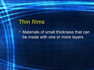
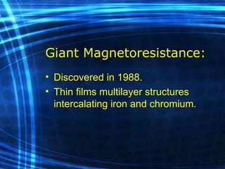
![Thin films and giant magnetoresistance Thin films: Gradual deposition of atoms in a substract Simple and multilayers [ iron – cobalt – nickel ] [ chromium – copper – ruthenium ] Giant magnetoresistance](https://image.slidesharecdn.com/nanoscience-5741/85/Nano-Science-80-320.jpg)

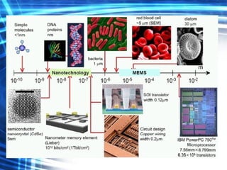
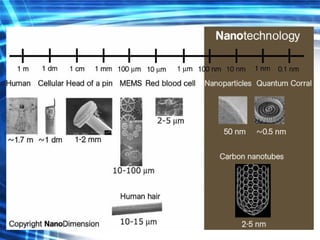
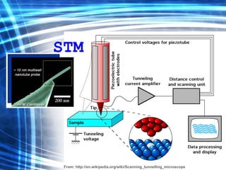
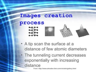
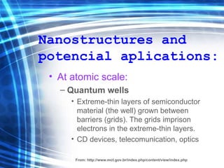
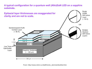
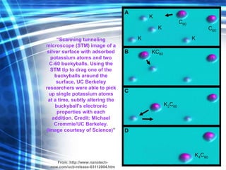
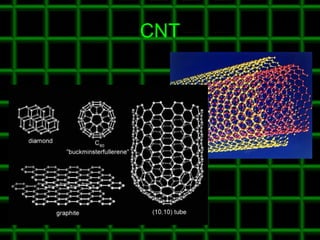
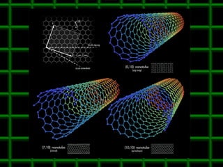
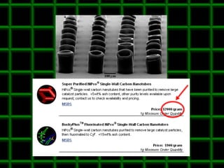
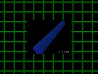
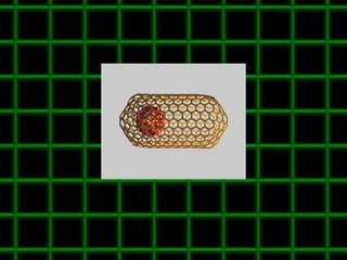
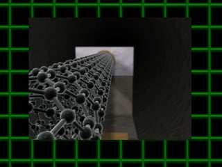
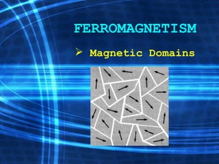
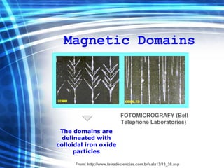
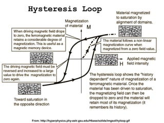
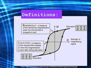
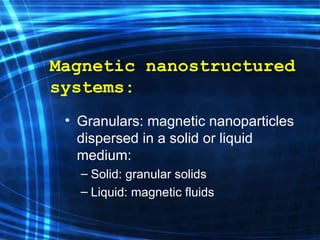
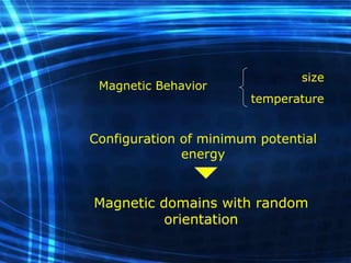
This document discusses nanoscience and nanotechnology concepts. It begins with an introduction to nanoscience topics like quantum effects at the nanoscale. It then discusses various nanostructures such as nanoparticles, nanotubes, thin films and their potential applications. The document also covers magnetic nanostructures such as ferromagnetism and magnetic domains. Measurement techniques like scanning tunneling microscopy are described. Finally, the document discusses thin film fabrication and the giant magnetoresistance effect in multilayer thin films.


