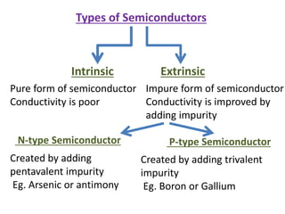
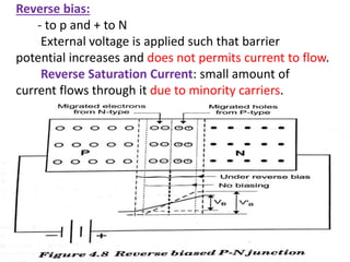
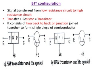
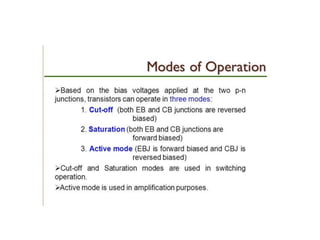
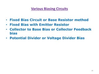
UNIT III – ANALOG
ELECTRONICS
Conductors: Conducts
currents, Valence and
conduction band overlap
Insulators: Does not
Conducts currents, Valence
and conduction band
separated by forbidden
energy gap
Semiconductor: Conductivity
is less than conductor and
greater than insulators
Types of Semiconductors
N-type Semiconductor P-type Semiconductor
Intrinsic Extrinsic
Pure form of semiconductor
Conductivity is poor
Impure form of semiconductor
Conductivity is improved by
adding impurity
Created by adding
pentavalent impurity
Eg. Arsenic or antimony
Created by adding trivalent
impurity
Eg. Boron or Gallium
PN junction diode
• Junction is formed between p type and n type is called pn
junction.
• It is called diode because it has two electrodes one for P
region called anode and other is N type called cathode
• P type- majority carriers - holes
• N type- majority carriers -free electrons
Diffusion: Charge carrier is moving from high concentration
area to low concentration area.
Junction voltage or barrier voltage: Existence of immobile
ions develops the potential difference across the junction
under equilibrium condition.
For germanium = 0.3 V & For silicon = 0.7 V
Operation of PN junction
Forward bias:
+ to p and – to N
External voltage applied is > than barrier potential
and cancels the potential and permits current to flow.
Reverse bias:
- to p and + to N
External voltage is applied such that barrier
potential increases and does not permits current to flow.
Reverse Saturation Current: small amount of
current flows through it due to minority carriers.
V-I Characteristics of PN junction
Forward bias:
• On varying voltage slowly, the barrier potential is
eliminated and current starts flowing called threshold
voltage or cut in voltage or knee voltage.
• As forward voltage applied increases beyond threshold
voltage, forward current increases exponentially.
Reverse bias:
• Breakdown of junction occurs results sudden rise in
reverse current. This current is called reverse
saturation current.
Applications of PN junction diode
• Switches
• Rectifiers
• Power Supplies
• Digital systems
Zener Diode
• If p and n region is heavily doped, the breakdown
voltage is reduced.
• If doping is heavy, reverse voltage is low then
electron can break from its bond. This effect is
called zener effect
• Diode exhibits zener effect is called zener
diode(heavily doped PN junction operates in
breakdown region)
Symbol of zener diode V-I characteristics
Applications of Zener diode
• As voltage regulator
• Protection of meters against damage of
accidental applications of excessive voltage.
Transistor types
BJT configuration
• Signal transferred from low resistance circuit to high
resistance circuit
• Transfer + Resistor = Transistor
• It consists of two back to back pn junction joined
together to form single piece of semiconductor
• Emitter- heavily doped
• Base-lightly doped
• Collector-moderately doped
IE = IB+IC
Applications of BJT
Common base
Input Characteristics
Output Characteristics
Current gain
Common Emitter
Input Characteristics Output Characteristics
Common Collector
α = IC / IE β = IC / IB
IE = IB+IC
α = β / (1+β) β = α / (1-α)
25
Transistor Biasing
The basic function of transistor is amplification. The process of raising the
strength of weak signal without any change in its general shape is referred as
faithful amplification. For faithful amplification it is essential that:-
1. Emitter-Base junction is forward biased
2. Collector- Base junction is reversed biased
3. Proper zero signal collector current
The proper flow of zero signal collector current and the maintenance of
proper collector emitter voltage during the passage of signal is called
transistor biasing.
26
BIAS STABILITY
 Through proper biasing, a desired quiescent operating point of the transistor
amplifier in the active region (linear region) of the characteristics is obtained. It is
desired that once selected the operating point should remain stable. The maintenance
of operating point stable is called Stabilisation.
 The selection of a proper quiescent point generally depends on the following factors:
(a) The amplitude of the signal to be handled by the amplifier and distortion level
in signal
(b) The load to which the amplifier is to work for a corresponding supply voltage
 The operating point of a transistor amplifier shifts mainly with changes in
temperature, since the transistor parameters — β, ICO and VBE (where the symbols carry
their usual meaning)—are functions of temperature.
27
The DC Operating Point
For a transistor circuit to amplify it must be properly biased with dc
voltages. The dc operating point between saturation and cutoff is
called the Q-point. The goal is to set the Q-point such that that it
does not go into saturation or cutoff when an a ac signal is applied.
28
Various Biasing Circuits
• Fixed Bias Circuit or Base Resistor method
• Fixed Bias with Emitter Resistor
• Collector to Base Bias or Collector Feedback
bias
• Potential Divider or Voltage Divider Bias
29
VCC
RC
C
E
B
VCC
R1
RE
R2
IE
IC
Ib
Potential Divider Bias Circuit
Rth = R1*R2 & Vth = Vcc R2
R1+R2 R1+R2
VCC
RC
C
E
B
VCC
R1
RE
R2
Rth = R1*R2 & Vth = Vcc R2
R1+R2 R1+R2
Rth = R1*R2 & Vth = Vcc R2
R1+R2 R1+R2
Rth = R1*R2 & Vth = Vcc R2
R1+R2 R1+R2
30
Summary
• The Q-point is the best point for operation of a
transistor for a given collector current.
• The purpose of biasing is to establish a stable
operating point (Q-point).
• The linear region of a transistor is the region of
operation within saturation and cutoff.
• Out of all the biasing circuits, potential divider bias
circuit provides highest stability to operating point.

Analog Electronics - Basics - Part-1

  • 1.
    UNIT III –ANALOG ELECTRONICS
  • 2.
    Conductors: Conducts currents, Valenceand conduction band overlap Insulators: Does not Conducts currents, Valence and conduction band separated by forbidden energy gap Semiconductor: Conductivity is less than conductor and greater than insulators
  • 3.
    Types of Semiconductors N-typeSemiconductor P-type Semiconductor Intrinsic Extrinsic Pure form of semiconductor Conductivity is poor Impure form of semiconductor Conductivity is improved by adding impurity Created by adding pentavalent impurity Eg. Arsenic or antimony Created by adding trivalent impurity Eg. Boron or Gallium
  • 4.
    PN junction diode •Junction is formed between p type and n type is called pn junction. • It is called diode because it has two electrodes one for P region called anode and other is N type called cathode • P type- majority carriers - holes • N type- majority carriers -free electrons
  • 5.
    Diffusion: Charge carrieris moving from high concentration area to low concentration area. Junction voltage or barrier voltage: Existence of immobile ions develops the potential difference across the junction under equilibrium condition. For germanium = 0.3 V & For silicon = 0.7 V
  • 6.
    Operation of PNjunction Forward bias: + to p and – to N External voltage applied is > than barrier potential and cancels the potential and permits current to flow.
  • 7.
    Reverse bias: - top and + to N External voltage is applied such that barrier potential increases and does not permits current to flow. Reverse Saturation Current: small amount of current flows through it due to minority carriers.
  • 8.
    V-I Characteristics ofPN junction Forward bias: • On varying voltage slowly, the barrier potential is eliminated and current starts flowing called threshold voltage or cut in voltage or knee voltage. • As forward voltage applied increases beyond threshold voltage, forward current increases exponentially.
  • 9.
    Reverse bias: • Breakdownof junction occurs results sudden rise in reverse current. This current is called reverse saturation current. Applications of PN junction diode • Switches • Rectifiers • Power Supplies • Digital systems
  • 10.
    Zener Diode • Ifp and n region is heavily doped, the breakdown voltage is reduced. • If doping is heavy, reverse voltage is low then electron can break from its bond. This effect is called zener effect • Diode exhibits zener effect is called zener diode(heavily doped PN junction operates in breakdown region)
  • 11.
    Symbol of zenerdiode V-I characteristics
  • 12.
    Applications of Zenerdiode • As voltage regulator • Protection of meters against damage of accidental applications of excessive voltage.
  • 13.
  • 14.
    BJT configuration • Signaltransferred from low resistance circuit to high resistance circuit • Transfer + Resistor = Transistor • It consists of two back to back pn junction joined together to form single piece of semiconductor
  • 15.
    • Emitter- heavilydoped • Base-lightly doped • Collector-moderately doped IE = IB+IC
  • 17.
  • 18.
  • 19.
  • 20.
  • 21.
  • 22.
  • 24.
    α = IC/ IE β = IC / IB IE = IB+IC α = β / (1+β) β = α / (1-α)
  • 25.
    25 Transistor Biasing The basicfunction of transistor is amplification. The process of raising the strength of weak signal without any change in its general shape is referred as faithful amplification. For faithful amplification it is essential that:- 1. Emitter-Base junction is forward biased 2. Collector- Base junction is reversed biased 3. Proper zero signal collector current The proper flow of zero signal collector current and the maintenance of proper collector emitter voltage during the passage of signal is called transistor biasing.
  • 26.
    26 BIAS STABILITY  Throughproper biasing, a desired quiescent operating point of the transistor amplifier in the active region (linear region) of the characteristics is obtained. It is desired that once selected the operating point should remain stable. The maintenance of operating point stable is called Stabilisation.  The selection of a proper quiescent point generally depends on the following factors: (a) The amplitude of the signal to be handled by the amplifier and distortion level in signal (b) The load to which the amplifier is to work for a corresponding supply voltage  The operating point of a transistor amplifier shifts mainly with changes in temperature, since the transistor parameters — β, ICO and VBE (where the symbols carry their usual meaning)—are functions of temperature.
  • 27.
    27 The DC OperatingPoint For a transistor circuit to amplify it must be properly biased with dc voltages. The dc operating point between saturation and cutoff is called the Q-point. The goal is to set the Q-point such that that it does not go into saturation or cutoff when an a ac signal is applied.
  • 28.
    28 Various Biasing Circuits •Fixed Bias Circuit or Base Resistor method • Fixed Bias with Emitter Resistor • Collector to Base Bias or Collector Feedback bias • Potential Divider or Voltage Divider Bias
  • 29.
    29 VCC RC C E B VCC R1 RE R2 IE IC Ib Potential Divider BiasCircuit Rth = R1*R2 & Vth = Vcc R2 R1+R2 R1+R2 VCC RC C E B VCC R1 RE R2 Rth = R1*R2 & Vth = Vcc R2 R1+R2 R1+R2 Rth = R1*R2 & Vth = Vcc R2 R1+R2 R1+R2 Rth = R1*R2 & Vth = Vcc R2 R1+R2 R1+R2
  • 30.
    30 Summary • The Q-pointis the best point for operation of a transistor for a given collector current. • The purpose of biasing is to establish a stable operating point (Q-point). • The linear region of a transistor is the region of operation within saturation and cutoff. • Out of all the biasing circuits, potential divider bias circuit provides highest stability to operating point.