Downloaded 319 times
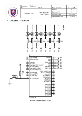
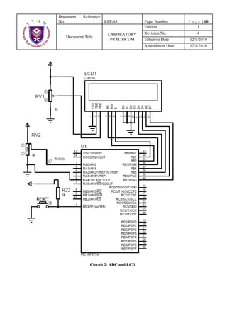

This document provides instructions for a laboratory experiment on a PIC microcontroller involving EEPROM, analog to digital conversion, and LCD display. The objectives are to understand EEPROM, ADC functionality and configuration. Experiments include writing and reading EEPROM, reading analog voltage with ADC and displaying on LCD, and programming a digital thermometer to read temperature from a sensor. Circuits include EEPROM with LEDs and ADC reading a potentiometer voltage to display on LCD. Exercises involve writing to all EEPROM addresses, displaying measured voltages, and programming a temperature display.