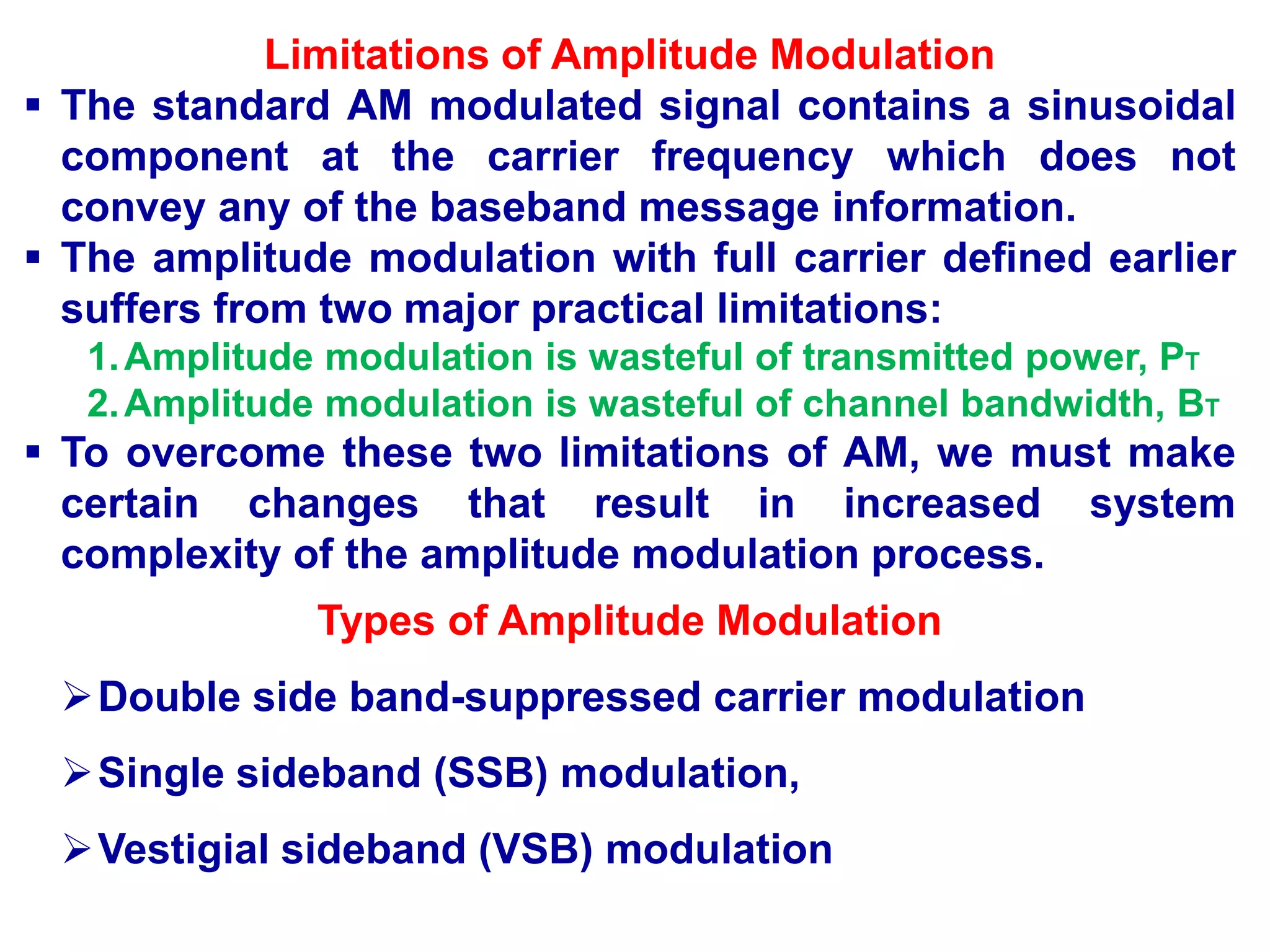
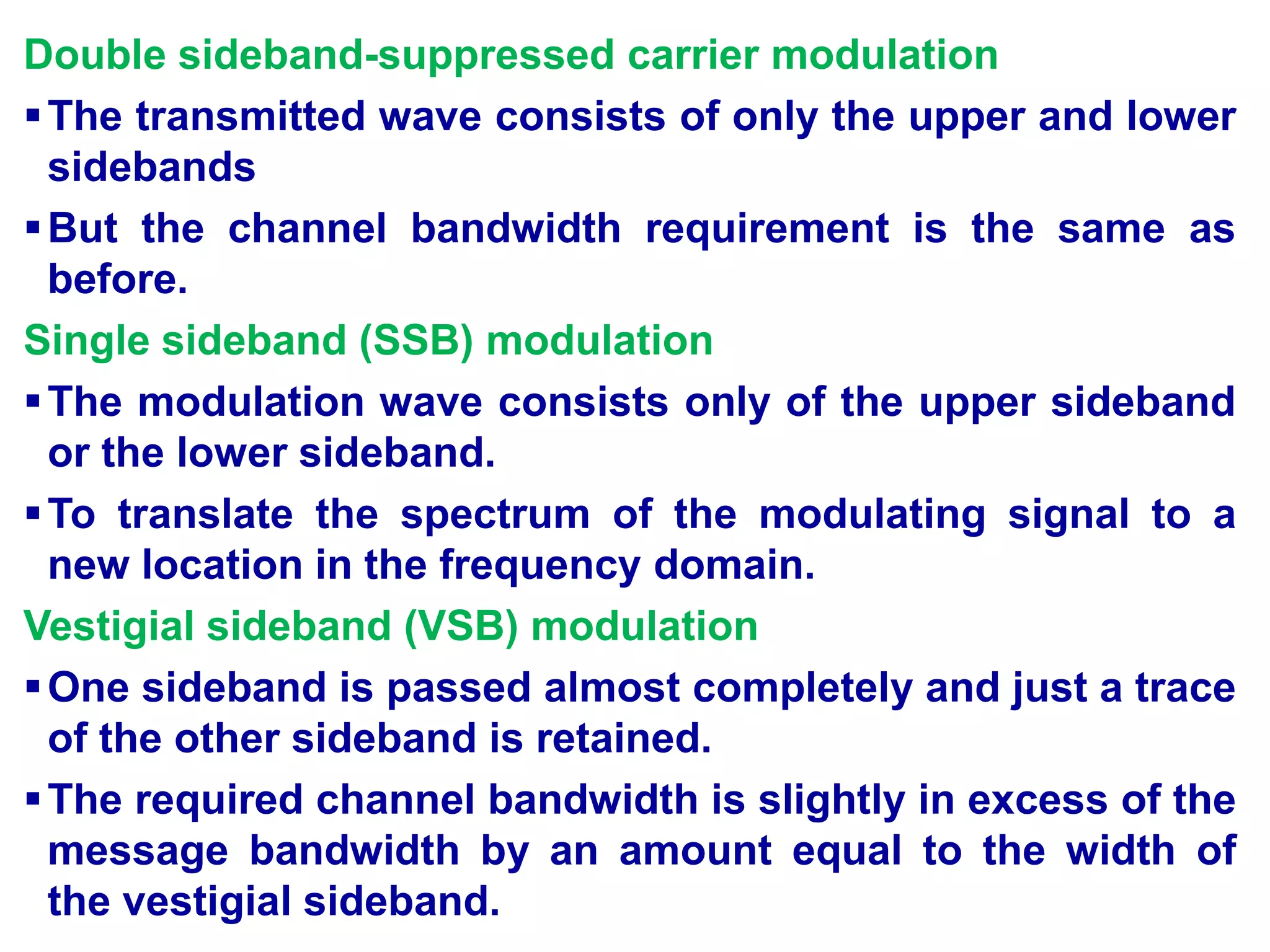
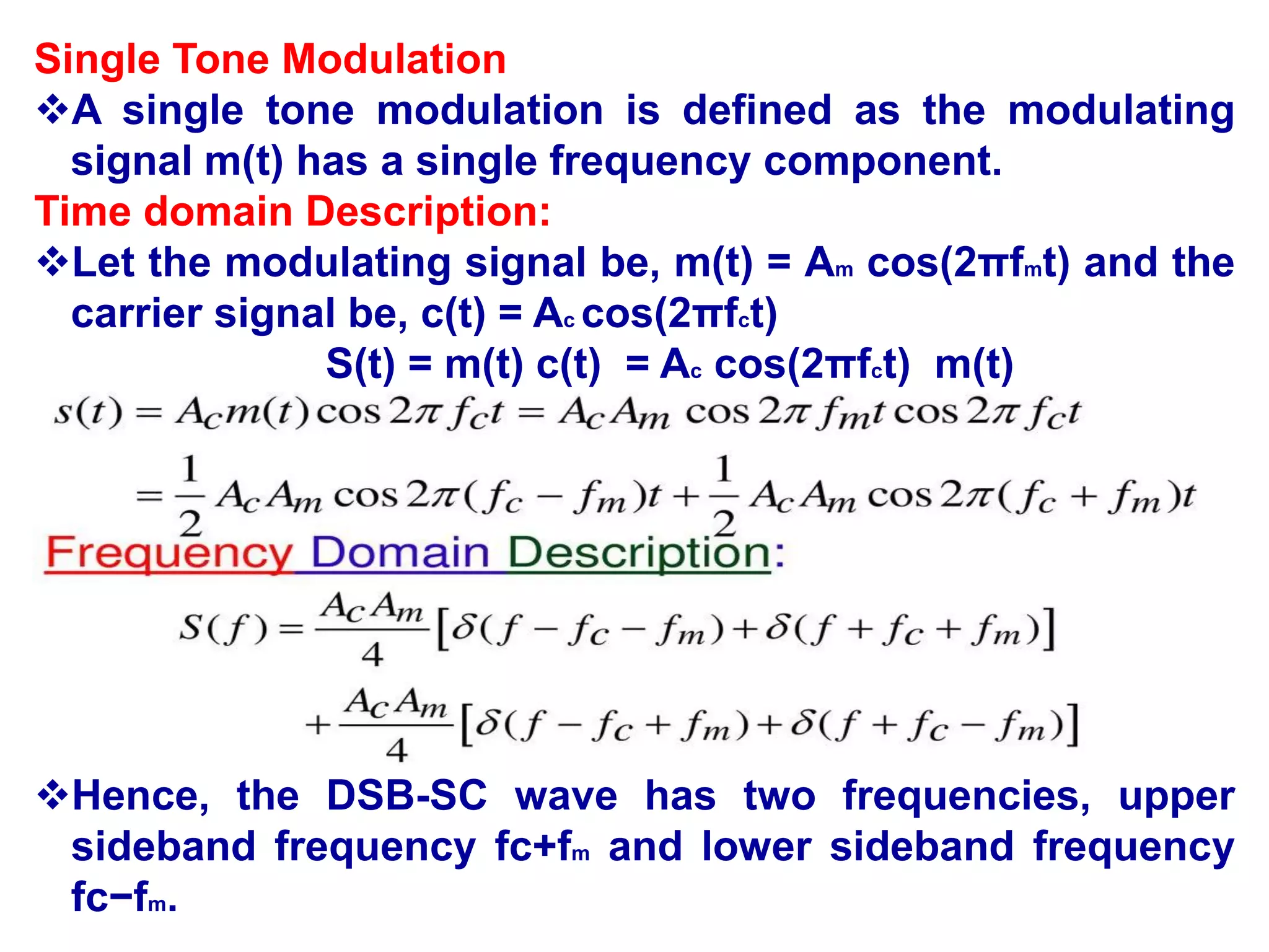
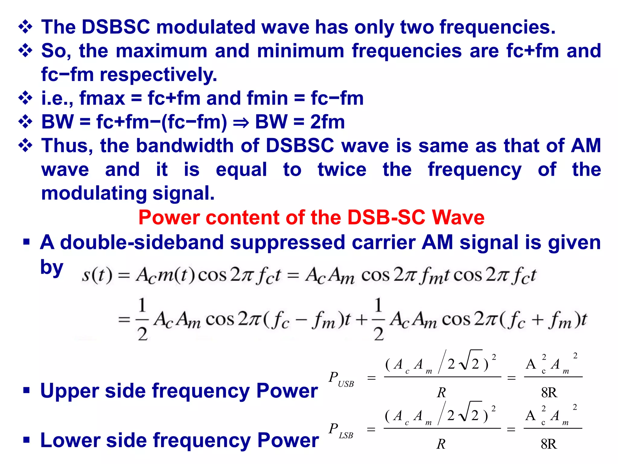
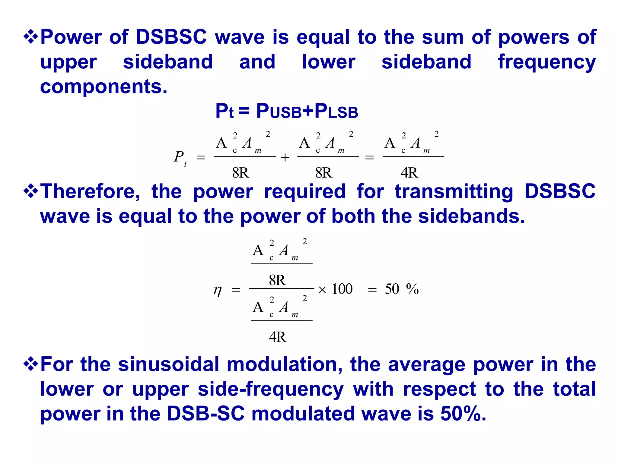
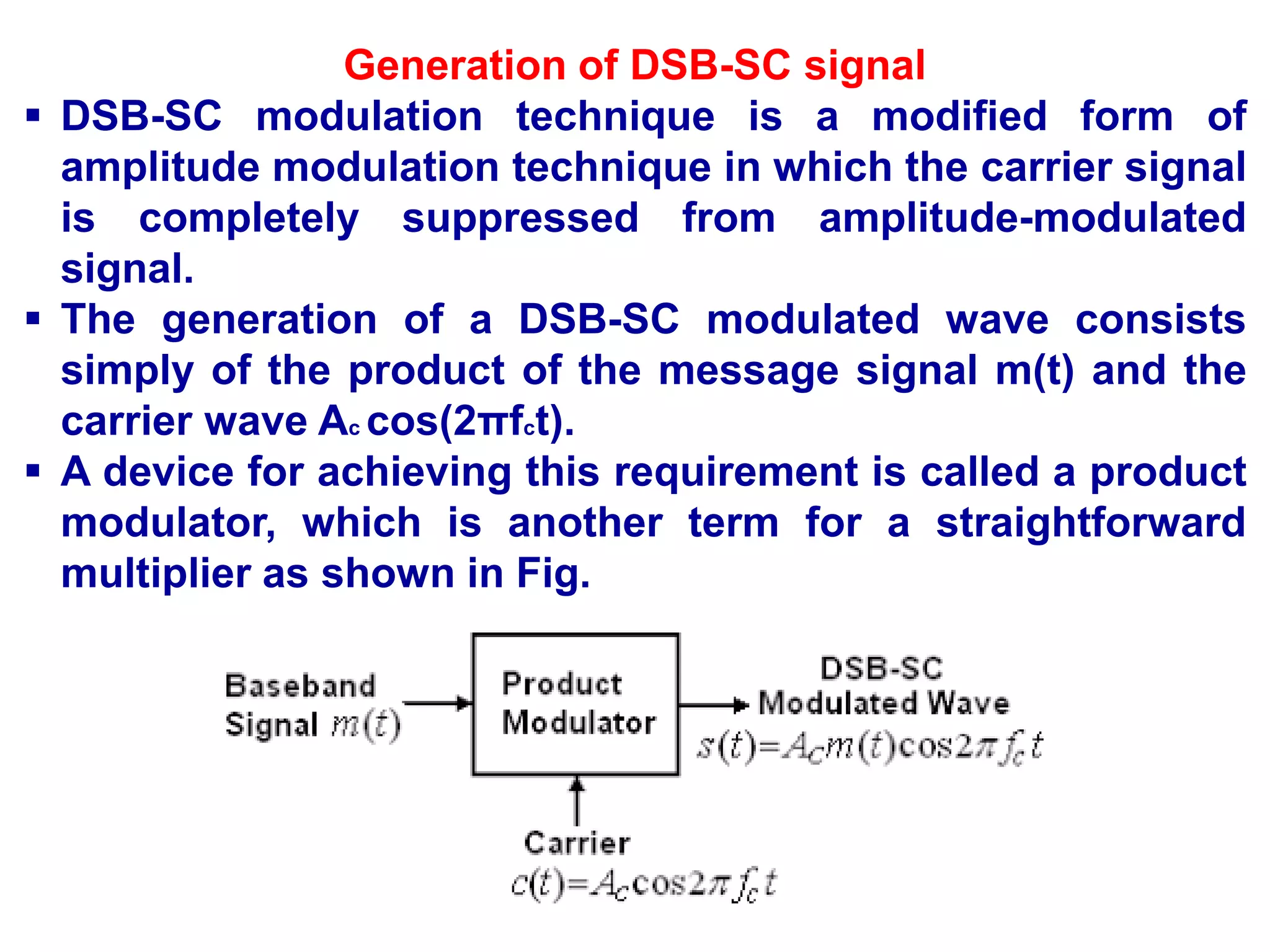
This document discusses various amplitude modulation techniques including DSBSC, SSB, and VSB modulation. It provides explanations of how to generate DSBSC waves using balanced modulators and ring modulators. It also describes coherent detection of DSBSC waves using synchronous detection and Costas loops. Methods for generating SSB signals using frequency and phase discrimination are outlined. VSB modulation is also introduced along with comparisons of different AM techniques. Limitations of standard AM are discussed and how more advanced modulation methods aim to overcome these limitations.
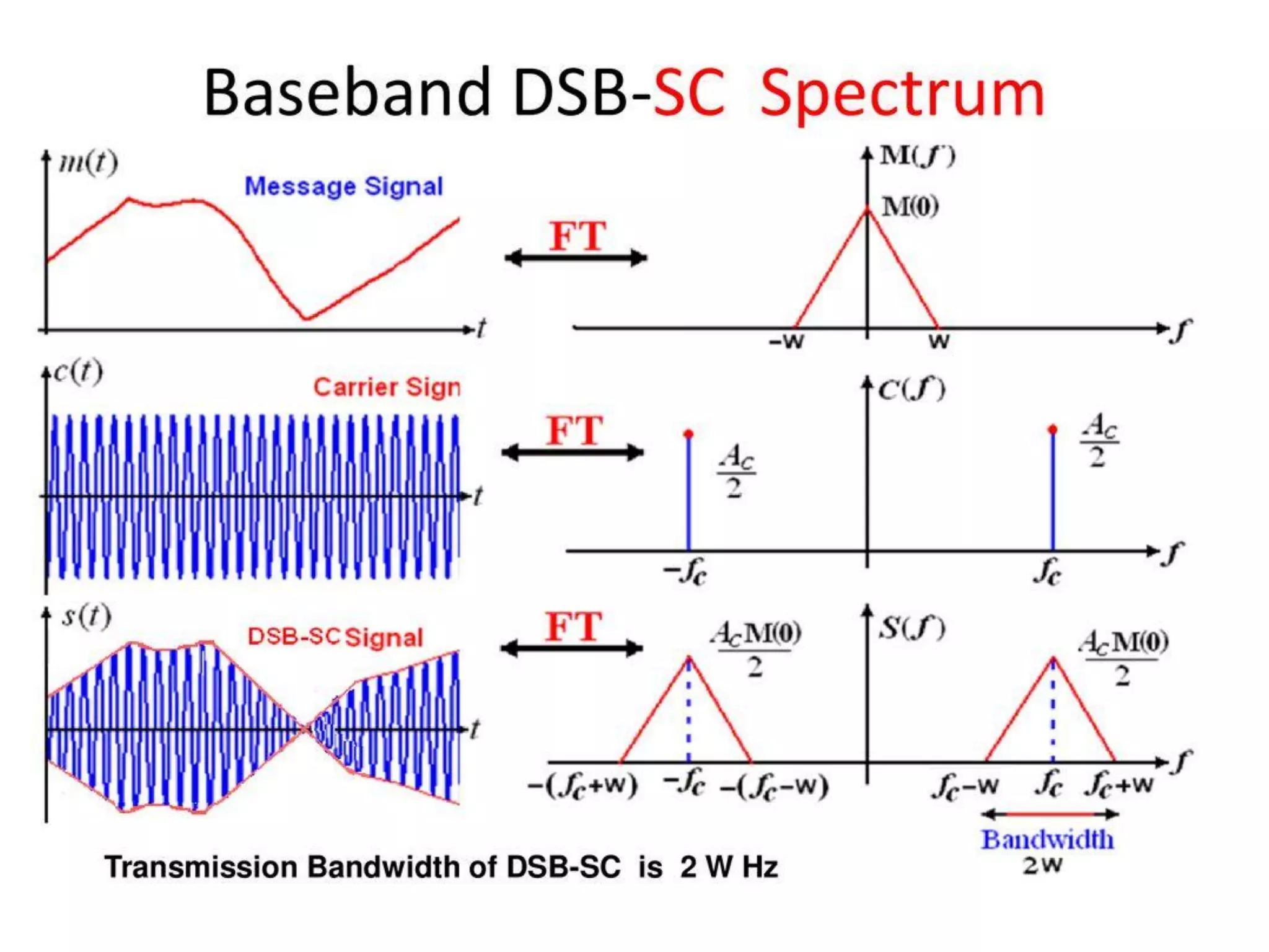
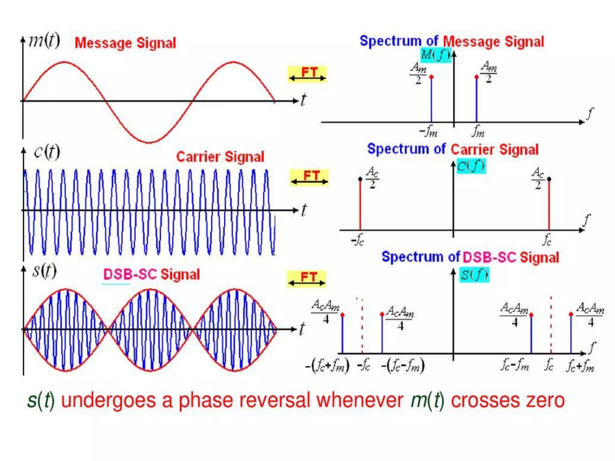
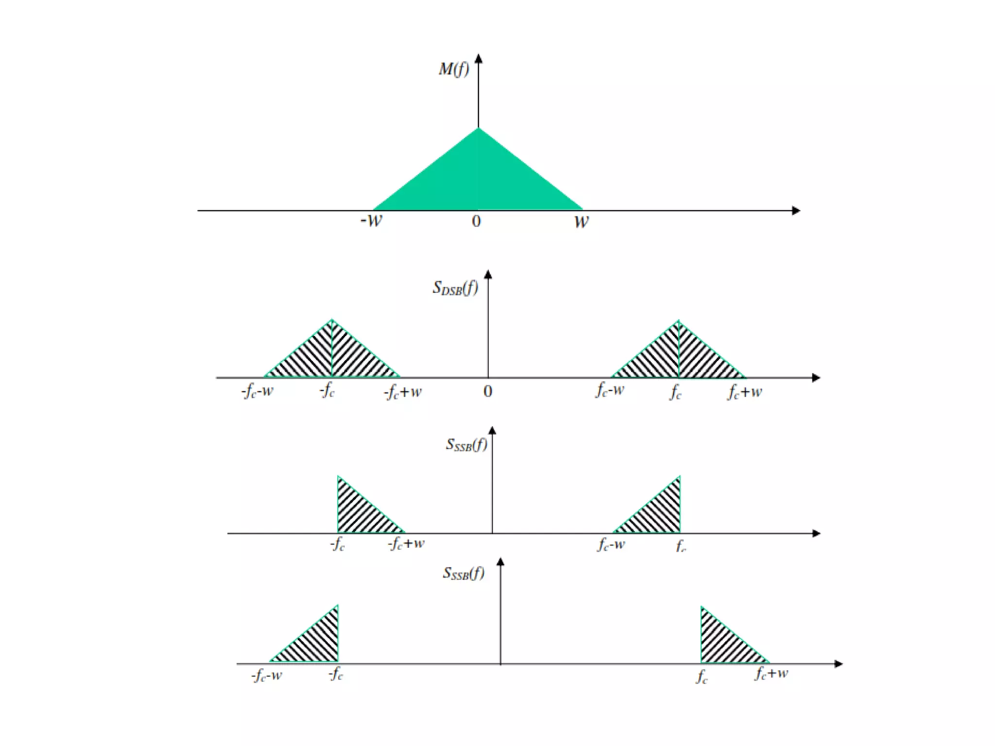
![Double sideband suppressed carrier (DSB-SC) modulation
To overcome the drawback of power wastage in AM wave,
suppress the carrier component from the modulated wave,
resulting in DSB-SC modulation.
A double-sideband suppressed carrier AM signal is
obtained by multiplying the message signal m(t) with the
carrier signal.
Let the modulating signal be,
m(t)=Amcos(2πfmt)
and the carrier signal be,
c(t) Ac cos(2πfct)
S(t) = m(t)c(t) S(t) = Ac cos(2πfct) m(t)
For the above equation Applying Fourier transform then
S(f) = Ac/2 [M(f – fc) + M(f + fc)]
The spectrum of DSB-SC modulated wave consists of
impulse functions located at fc ±fm and − fc ±fm.](https://image.slidesharecdn.com/acuint202-02-2023-1-230627153417-04e1aa31/75/AC-UINT-2-02-02-2023-1-pdf-5-2048.jpg)
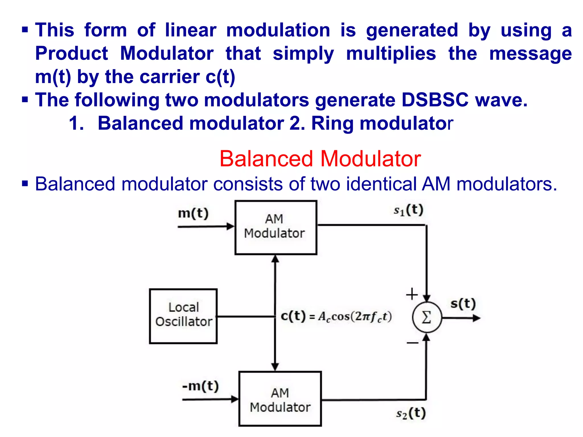
![ These two modulators are arranged in a balanced
configuration in order to suppress the carrier signal.
Hence, it is called as Balanced modulator.
The same carrier signal c(t) = Ac cos(2πfct) is applied as
one of the inputs to these two AM modulators.
The modulating signal m(t) is applied as another input to
the upper AM modulator.
Whereas, the modulating signal m(t) with opposite
polarity, i.e., −m(t) is applied as another input to the lower
AM modulator.
Output of the upper AM modulator is
s1(t)=Ac[1+kam(t)]cos(2πfct)
Output of the lower AM modulator is
s2(t)=Ac[1−kam(t)]cos(2πfct)
The summer block is used to perform this operation.
s1(t) with positive sign and s2(t) with negative sign are
applied as inputs to summer block.](https://image.slidesharecdn.com/acuint202-02-2023-1-230627153417-04e1aa31/75/AC-UINT-2-02-02-2023-1-pdf-13-2048.jpg)
![ Thus, the summer block produces an output s(t) which is
the difference of s1(t) and s2(t).
s(t) = Ac[1+kam(t)]cos(2πfct)−Ac[1−kam(t)]cos(2πfct)
⇒s(t)=Accos(2πfct)+Ackam(t)cos(2πfct)−Accos(2πfct)+
Ackam(t)cos(2πfct) ⇒s(t)=2Ackam(t)cos(2πfct)
The standard equation of DSBSC wave is
s(t)=Acm(t)cos(2πfct)
By comparing the output of summer block with the
standard equation of DSBSC wave, we will get the scaling
factor as 2ka.
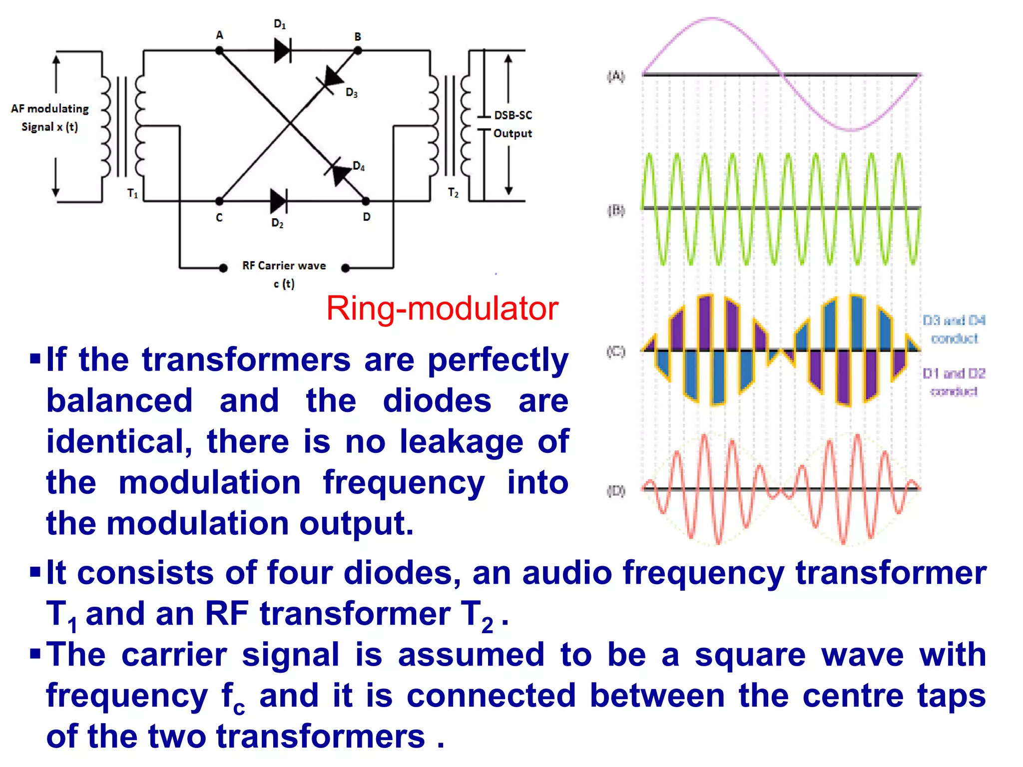
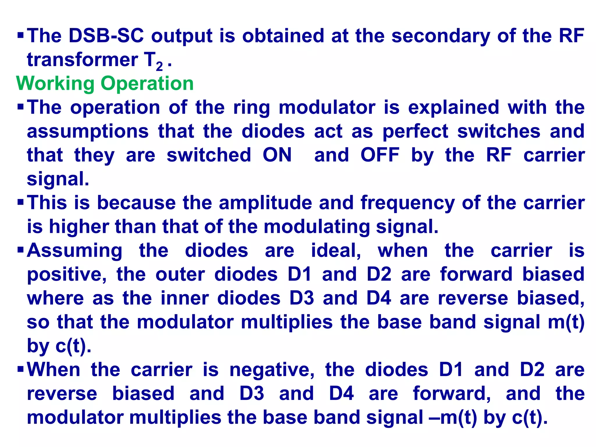
Ring modulator
The four diodes form a ring in which they all point in the
same direction.
Ring modulator is one of the most useful product
modulator, well suited for generating a DSB-SC wave.
The diodes are controlled by square-wave carrier c(t) of
frequency fc , which is applied longitudinally by means of
two center-tapped transformers.](https://image.slidesharecdn.com/acuint202-02-2023-1-230627153417-04e1aa31/75/AC-UINT-2-02-02-2023-1-pdf-14-2048.jpg)
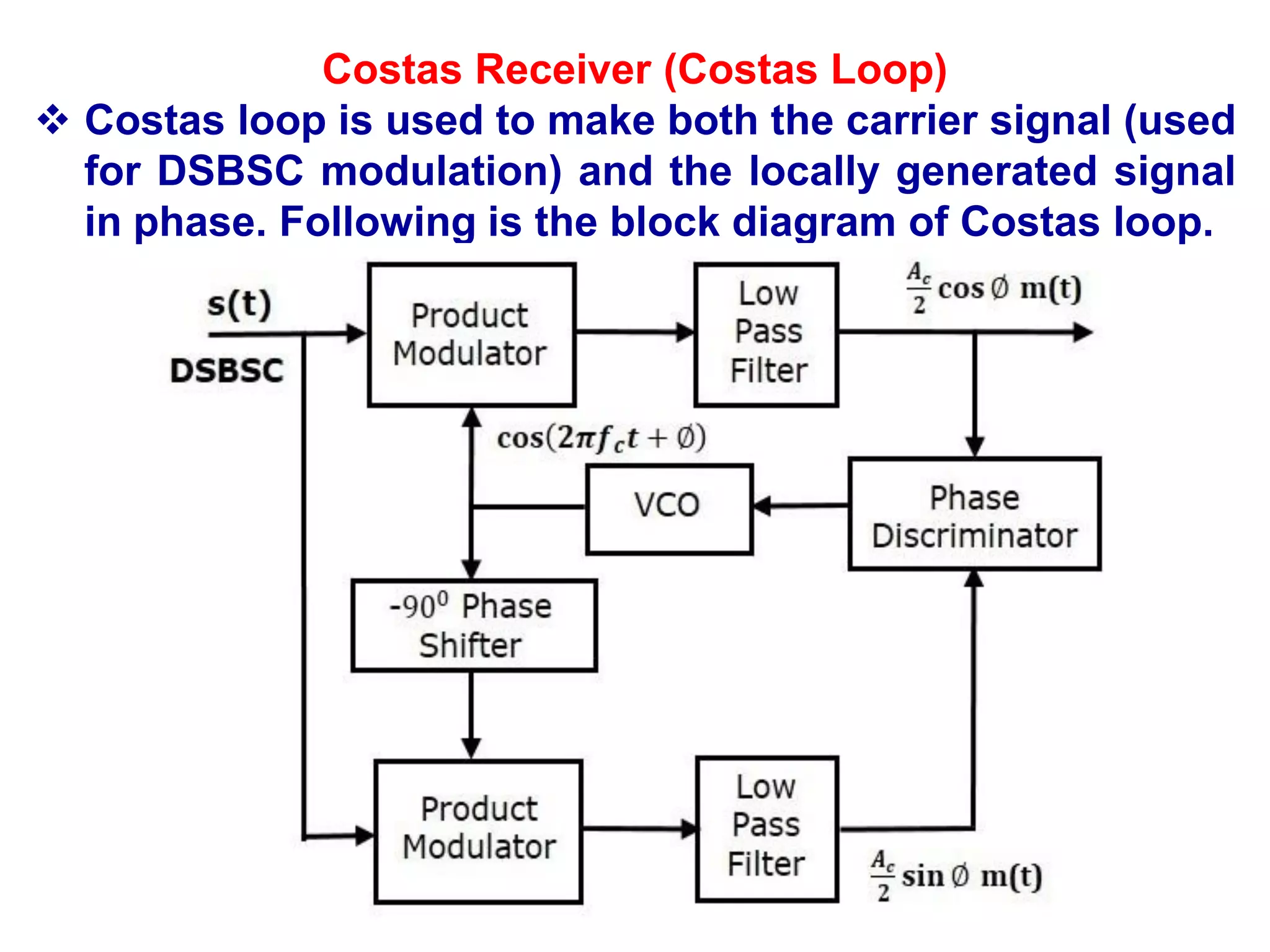
![COHERENT (SYNCHRONOUS) DETECTOR
It is assumed that the local oscillator signal is exactly
coherent or synchronized, in both frequency and phase,
with carrier wave c(t) used in the product modulator to
generate s(t).
This method of demodulation is known as coherent
detection or synchronous demodulation.
The message signal m(t) may be recovered from a DSB -
SC modulated wave s(t) with a locally generated
sinusoidal wave and then low-pass filtering the product
as shown in Fig
We know that, S(t) = m(t )c(t)
S(t) = m(t) cos(2πfct)
t
f
t
f
t
m
t
s c
c
c
2
cos
]
2
cos
)
(
[
)
(
t
f
t
m
t
m
t
f
t
m
t
s c
c
c
4
cos
)
(
)
(
]
4
cos
1
[
)
(
)
( 2
1
2
1
2
1
)
(
)
( 2
1
t
m
t
s o
](https://image.slidesharecdn.com/acuint202-02-2023-1-230627153417-04e1aa31/75/AC-UINT-2-02-02-2023-1-pdf-18-2048.jpg)
![DSB-SC modulated spectrum is multiplied using local
oscillator.
This resulting signal is passed through the Low Pass Filter
to retrieve back the message signal.
The first term in Eq. is removed by low-pass filter,
provided that the cut-off frequency of this filter is greater
than w but less than 2𝑓𝑐 - w. This is satisfied by choosing 𝑓
𝑐 >w
Information is contained in the first part i.e. (1/2)m(t) which
is low pass filtered and extracted.
S(t) = m(t)c(t)
S(t) = cos(2πfct) m(t)
)
2
(
cos
]
2
cos
)
(
[
)
(
t
f
A
t
f
t
m
t
v c
c
c
)
2
(
cos
)
(
cos
)
(
)
(
cos
)
(
)
2
(
cos
)
(
)
(
2
2
2
2
t
t
m
t
m
t
m
t
t
m
t
v
c
A
A
A
c
A
c
c
c
c
cos
)
(
)
( 2
c
A
o
t
m
t
v ](https://image.slidesharecdn.com/acuint202-02-2023-1-230627153417-04e1aa31/75/AC-UINT-2-02-02-2023-1-pdf-19-2048.jpg)
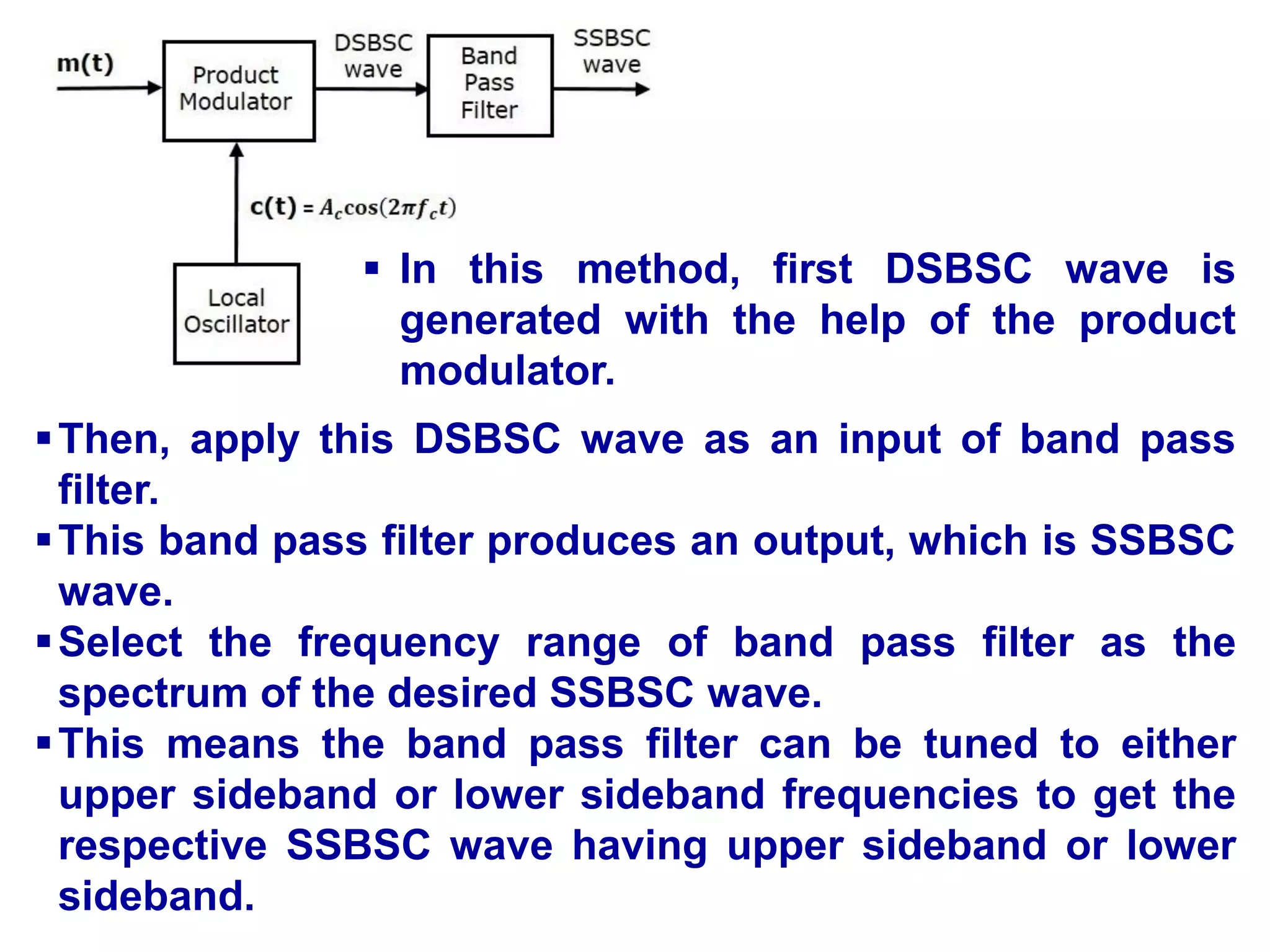
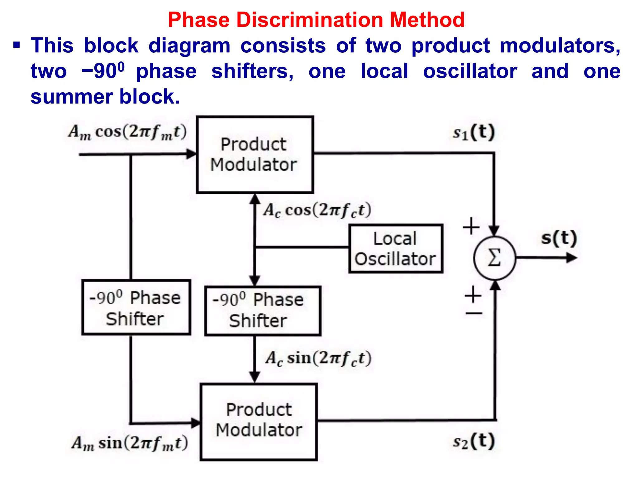
![ The product modulator produces an output, which is the
product of two inputs.
The −900 phase shifter produces an output, which has a
phase lag of −900 with respect to the input.
The local oscillator is used to generate the carrier signal.
Summer block produces an output, which is either the
sum of two inputs or the difference of two inputs based
on the polarity of inputs.
The modulating signal Am cos(2πfmt) and the carrier
signal Ac cos(2πfct) are directly applied as inputs to the
upper product modulator.
So, the upper product modulator produces an output,
which is the product of these two inputs.
The output of upper product modulator is
s1(t) = AmAc cos(2πfmt) cos(2πfct)
⇒s1(t) = AmAc/2 {cos[2π(fc+fm)t] + cos[2π(fc−fm)t]}](https://image.slidesharecdn.com/acuint202-02-2023-1-230627153417-04e1aa31/75/AC-UINT-2-02-02-2023-1-pdf-34-2048.jpg)
![ The modulating signal Am cos(2πfmt) and the carrier
signal Ac cos(2πfct) are phase shifted by −900 before
applying as inputs to the lower product modulator.
So, the lower product modulator produces an output,
which is the product of these two inputs.
The output of lower product modulator is
s2(t) = AmAc cos(2πfmt−900) cos(2πfct−900)
⇒ s2(t) = AmAc sin(2πfmt) sin(2πfct)
⇒s2(t)=AmAc/2{cos[2π(fc−fm)t] − cos[2π(fc+fm)t]}
Add s1(t) and s2(t) in order to get the SSBSC modulated
wave s(t) having a lower sideband.
s(t) = AmAc/2 {cos[2π(fc+fm)t] + cos[2π(fc−fm)t]} +
AmAc/2 {cos[2π(fc−fm)t] − cos[2π(fc+fm)t]}
⇒ s(t )= AmAc cos[2π(fc−fm)t]
Subtract s2(t) from s1(t) in order to get the SSBSC
modulated wave s(t) having a upper sideband.](https://image.slidesharecdn.com/acuint202-02-2023-1-230627153417-04e1aa31/75/AC-UINT-2-02-02-2023-1-pdf-35-2048.jpg)
![s(t)=AmAc/2 {cos[2π(fc+fm)t] + cos[2π(fc−fm)t]} −
AmAc/2 {cos[2π(fc−fm)t] − cos[2π(fc+fm)t]}
⇒ s(t) = AmA ccos[2π(fc+fm)t]
Hence, by properly choosing the polarities of inputs at
summer block, we will get SSBSC wave having a upper
sideband or a lower sideband.
Coherent Detector
The process of extracting an original message signal
from SSBSC wave is known as detection or
demodulation of SSBSC.
Coherent detector is used for demodulating SSBSC
wave.
Here, the same carrier signal (which is used for
generating SSBSC wave) is used to detect the message
signal.
Hence, this process of detection is called
as coherent or synchronous detection.](https://image.slidesharecdn.com/acuint202-02-2023-1-230627153417-04e1aa31/75/AC-UINT-2-02-02-2023-1-pdf-36-2048.jpg)
![ In this process, the message signal can be extracted from
SSBSC wave by multiplying it with a carrier, having the
same frequency and the phase of the carrier used in
SSBSC modulation.
Consider the following SSBSC wave having a lower
sideband.
s(t) = AmAc/2 cos[2π(fc−fm)t]
The output of the local oscillator isc(t) = Ac cos(2πfct)
The output of product modulator as v(t) = s(t) c(t)
Substitute s(t) and c(t) values in the above equation.
The resulting signal is
then passed through a
Low Pass Filter.
The output of this filter is
the desired message
signal.](https://image.slidesharecdn.com/acuint202-02-2023-1-230627153417-04e1aa31/75/AC-UINT-2-02-02-2023-1-pdf-37-2048.jpg)
![v(t) = AmAc/2 cos[2π(fc−fm)t] Accos(2πfct)
= AmAc
2/2 cos[2π(fc−fm)t] cos(2πfct)
= AmAc
2/4 {cos[2π(2fc−fm)] + cos(2πfm)t}
v(t) = AmAc
2/4 cos(2πfmt) + AmAc
2/4 cos[2π(2fc−fm)t]
In the above equation, the first term is the scaled
version of the message signal.
It can be extracted by passing the above signal through
a low pass filter.
Therefore, the output of low pass filter is
v0(t) = AmAc
2/4cos(2πfmt)
Here, the scaling factor is Ac
2/4.](https://image.slidesharecdn.com/acuint202-02-2023-1-230627153417-04e1aa31/75/AC-UINT-2-02-02-2023-1-pdf-38-2048.jpg)
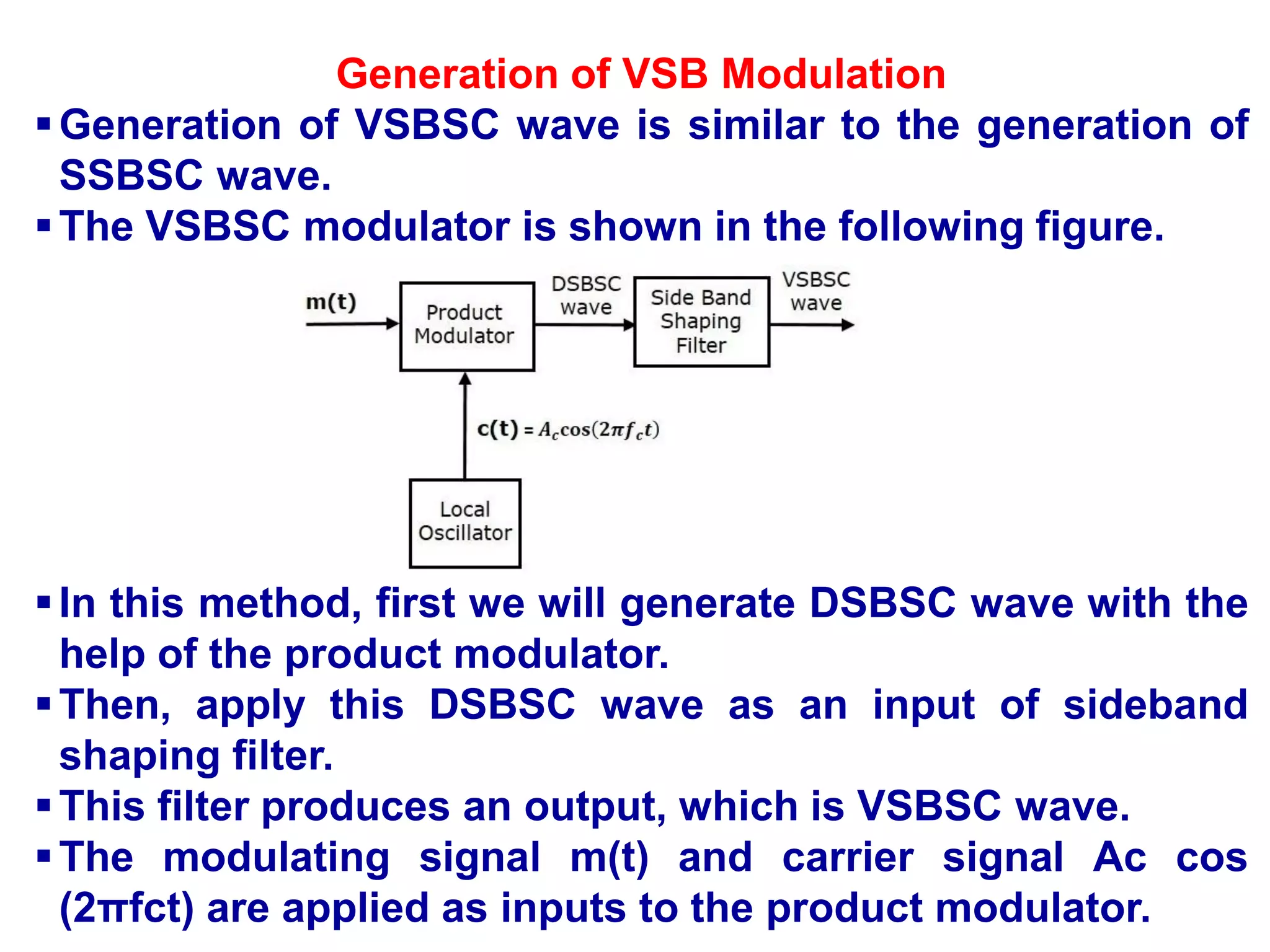
![ Hence, the product modulator produces an output, which
is the product of these two inputs.
Therefore, the output of the product modulator is
v(t)=Accos(2πfct)m(t)
Apply Fourier transform on both sides
V(f)=Ac/2[M(f−fc)+M(f+fc)]
The above equation represents the equation of DSBSC
frequency spectrum.
Let the transfer function of the sideband shaping filter
be H(f).
This filter has the input v(t) and the output is VSBSC
modulated wave s(t).
The Fourier transforms of v(t) and s(t) are V(f) and S(f)
respectively.
Mathematically, we can write S(f) as S(f)=V(f)H(f)
Substitute V(f) value in the above equation.
S(f)=Ac/2[M(f−fc)+M(f+fc)]H(f)](https://image.slidesharecdn.com/acuint202-02-2023-1-230627153417-04e1aa31/75/AC-UINT-2-02-02-2023-1-pdf-42-2048.jpg)
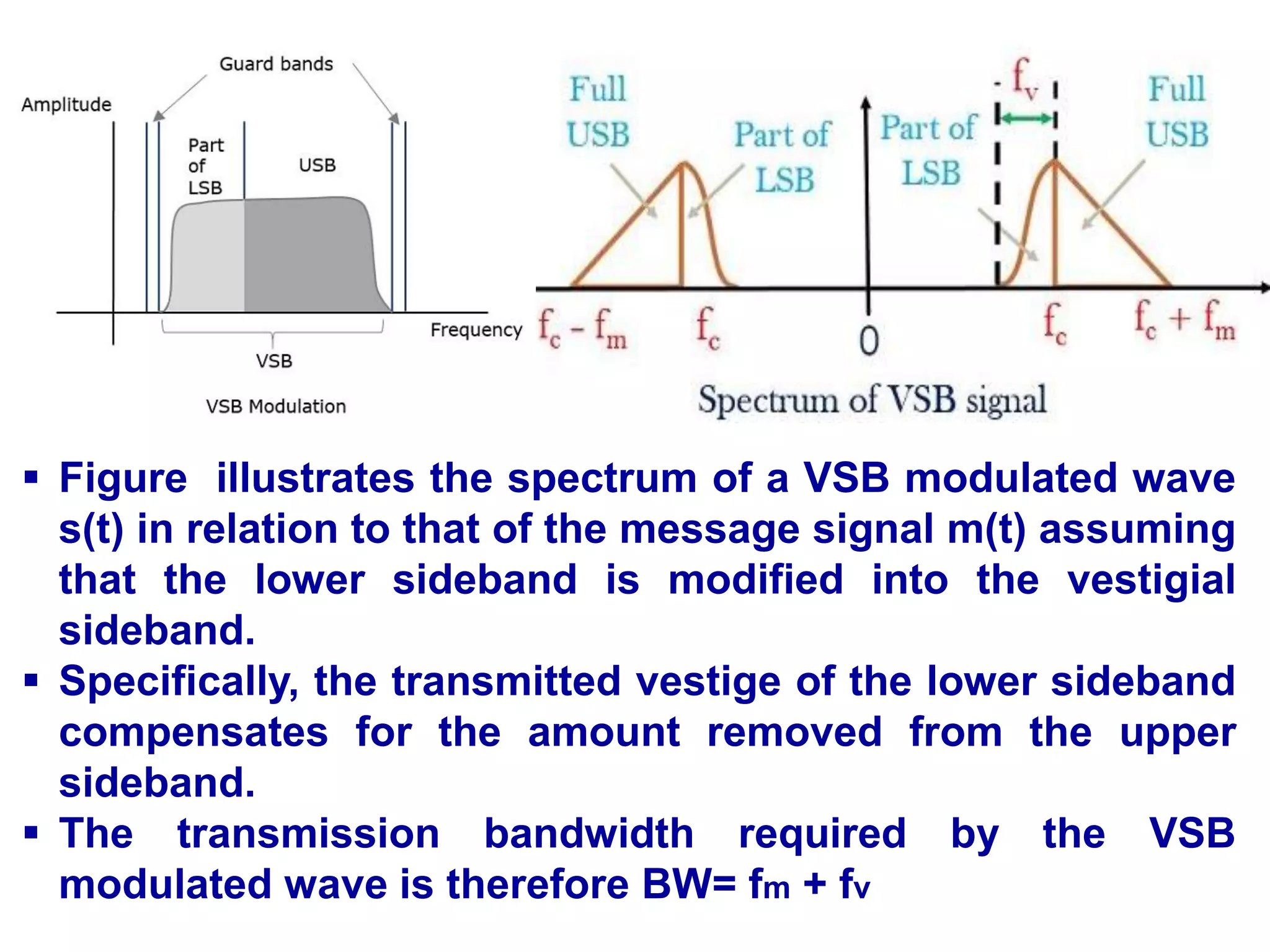
![The above equation represents the equation of VSBSC
frequency spectrum.
The condition for frequency response of filter is
[H(f−fc)+H(f+fc)]=1
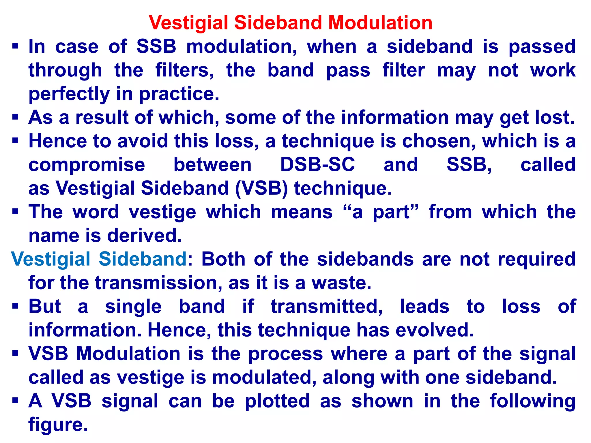
Detection of VSB Modulation
Demodulation of VSBSC wave is similar to the
demodulation of SSBSC wave.
Here, the same carrier signal (which is used for generating
VSBSC wave) is used to detect the message signal.
Hence, this process of detection is called
as coherent or synchronous detection.
The VSBSC demodulator is shown in the following figure.](https://image.slidesharecdn.com/acuint202-02-2023-1-230627153417-04e1aa31/75/AC-UINT-2-02-02-2023-1-pdf-43-2048.jpg)
![The resulting signal is then passed through a Low Pass
Filter.
The output of this filter is the desired message signal.
Let the VSBSC wave be s(t) and the carrier signal
is Accos(2πfct).
From the figure, we can write the output of the product
modulator as v(t)=Accos(2πfct)s(t)
Apply Fourier transform on both sides
V(f)=Ac/2[S(f−fc)+S(f+fc)]
We know that S(f)=Ac/2[M(f−fc)+M(f+fc)]H(f)
In this process, the message signal can
be extracted from VSBSC wave by
multiplying it with a carrier, which is
having the same frequency and the phase
of the carrier used in VSBSC modulation.](https://image.slidesharecdn.com/acuint202-02-2023-1-230627153417-04e1aa31/75/AC-UINT-2-02-02-2023-1-pdf-44-2048.jpg)
![From the above equation, let us find S(f−fc) and S(f+fc).
⇒S(f−fc)=Ac/2[M(f−2fc)+M(f)]H(f−fc)
⇒S(f+fc)=Ac/2[M(f)+M(f+2fc)]H(f+fc)
Substitute, S(f−fc) and S(f+fc) values in V(f).
V(f)=Ac/2[Ac/2[M(f−2fc)+M(f)]H(f−fc)+
Ac/2[M(f)+M(f+2fc)]H(f+fc)]
⇒V(f)=Ac/4 M(f)[H(f−fc)+H(f+fc)]+
Ac/4[M(f−2fc)H(f−fc)+M(f+2fc)H(f+fc)]
In the above equation, the first term represents the scaled
version of the desired message signal frequency
spectrum.
It can be extracted by passing the above signal through a
low pass filter.
V0(f)=Ac/4 M(f)[H(f−fc)+H(f+fc)]
The condition for frequency response of filter is
[H(f−fc)+H(f+fc)]=1
Therefore V0(f)=Ac/4M(f) Apply Inverse Fourier transform
on both sides v0(t)=Ac/4m(t)](https://image.slidesharecdn.com/acuint202-02-2023-1-230627153417-04e1aa31/75/AC-UINT-2-02-02-2023-1-pdf-45-2048.jpg)