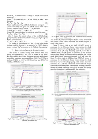
The document describes a modified Dickson charge pump design that reduces power consumption during input clock transitions. A PMOS transistor is added in series with each capacitor stage to increase the time constant, slowing the charge transfer. This reduces power from 340.5uW to 28.85uW at no load for the Dickson versus modified design. Output voltages are similar but slightly lower for the modified design. At 10MOhm and 40MOhm loads, power savings during transitions are also realized compared to the standard Dickson design while maintaining comparable output voltages. In conclusion, the modified design successfully reduces transition power consumption without significantly impacting output voltage.
![Diode Based Charge Pump Design using 0.35µm
Technology
Muhammad Adeel Ansari, Waqar Ahmad, Qiang Chen, Li-Rong Zheng
School of Information and Communication Technology,
KTH (Royal Institute of Technology), Forum 120, 164 40
Stockholm- Kista, Sweden.
{maansari,ahmadw,qchen,lirong}@kth.se
Abstract—A high voltage charge pump design is being presented Similar method is applied and presented in this paper, by
in this paper. The design is based on Dickson charge pump, slowing the charge transfer during the input clocks transition
constructed with diodes by using AMS 0.35µm technology. The where the change of voltage and the current is very fast. Rate
innovation is made in Dickson charge pump i.e. charge control of change of input clock during the transition is 0.2V/nS with
PMOS transistor is used in each stage of charge pump. PMOS the similar rate of change of current, to charge the capacitor
transistor is used in series with charging capacitor which reduces
and store the electric field in it. PMOS is being placed in
the power consumption during the clock transition by controlling
the time constant of each stage. The resistance between drain to series with charging capacitor in the Dickson charge pump to
source of PMOS transistor increases the time constant during the increase the time constant as the resistance in series is
charging of the capacitor placed in each stage of charge pump. increased by the drain to source resistance of PMOS.
The output voltage of about 5.693V is achieved by the six stages Therefore the charge transfer during the clock transition is
of Dickson charge pump at no-load which reduces to 5.537V with being slowed down and the power consumption is being
the six stages of proposed charge pump but the power during the reduced during the input clock transition. Effect of the PMOS
input clock transition is reduced from 340.5µw (consumed by transistor on power consumption during the input clock
Dickson charge pump) to 28.85 µW (consumed by the proposed transition is being presented as figure 1. It is shown by the
modified charge pump). Some other results are also discussed in
figure 1 that the power consumption is 483.7µW during the
this paper, which are achieved on different load resistances.
input clock transition without charge control transistor
whereas the power consumption during the input clock
Keywords-component transition is reduced to 61.85µW with charge controlling
High Voltage DC Output; DC-DC Converter; Charge Pump; Diode PMOS transistor. Detailed results will be discussed later in
based Charge Pump; Dickson Charge Pump, Input Clock this paper.
Transition.
I. INTRODUCTION
The charging of a capacitor is an exponential process and
follows the mathematical equation given as[1]:
Charging of capactior Vc(t) = Vin (1-e-t/τ) (i)
Where “t” is the charging time and “τ” is the charging time
constant. Similarly, discharging of a capacitor is also an
exponential process and follows the mathematical equation
given as[1]:
Discharging of capacitor Vc(t) = V0e-t/τ (ii)
Above equations of charging and discharging of a capacitor
have exponential e-t/τ function for charging and discharging
which depends on the time “t” and time constant “τ”. Time
constant of a capacitor can be calculated mathematically by Fig. 1. Power Consumption by the charge pump with and without
the equation given as: charge control transistor.
τ = RC (iii) In this paper, section II discusses the previous work,
Where “R” is the resistance in series of capacitor during section III discusses the Dickson charge pump design, section
the charging or discharging and “C” is the capacitance of the IV discusses the Dickson charge pump with charge controlling
capacitor to charge or discharge. transistors, section V discusses the results with graphical
If the resistance “R” is increased the charging time and the representation, section VI concluded the discussion in the light
discharging time of a capacitor can be increased and the of results achieved in this exercise and at the end of this paper
charging and discharging of the capacitor can be controlled by related references are given for those readers who would like
time constant. to read more about this part of the research.
1
978-1-4244-8971-8/10$26.00 c 2010 IEEE](https://image.slidesharecdn.com/84-101202234924-phpapp02/85/84-1-320.jpg)
![Diode Based Charge Pump Design using 0.35µm
Technology
Muhammad Adeel Ansari, Waqar Ahmad, Qiang Chen, Li-Rong Zheng
School of Information and Communication Technology,
KTH (Royal Institute of Technology), Forum 120, 164 40
Stockholm- Kista, Sweden.
{maansari,ahmadw,qchen,lirong}@kth.se
Abstract—A high voltage charge pump design is being presented Similar method is applied and presented in this paper, by
in this paper. The design is based on Dickson charge pump, slowing the charge transfer during the input clocks transition
constructed with diodes by using AMS 0.35µm technology. The where the change of voltage and the current is very fast. Rate
innovation is made in Dickson charge pump i.e. charge control of change of input clock during the transition is 0.2V/nS with
PMOS transistor is used in each stage of charge pump. PMOS the similar rate of change of current, to charge the capacitor
transistor is used in series with charging capacitor which reduces
and store the electric field in it. PMOS is being placed in
the power consumption during the clock transition by controlling
the time constant of each stage. The resistance between drain to series with charging capacitor in the Dickson charge pump to
source of PMOS transistor increases the time constant during the increase the time constant as the resistance in series is
charging of the capacitor placed in each stage of charge pump. increased by the drain to source resistance of PMOS.
The output voltage of about 5.693V is achieved by the six stages Therefore the charge transfer during the clock transition is
of Dickson charge pump at no-load which reduces to 5.537V with being slowed down and the power consumption is being
the six stages of proposed charge pump but the power during the reduced during the input clock transition. Effect of the PMOS
input clock transition is reduced from 340.5µw (consumed by transistor on power consumption during the input clock
Dickson charge pump) to 28.85 µW (consumed by the proposed transition is being presented as figure 1. It is shown by the
modified charge pump). Some other results are also discussed in
figure 1 that the power consumption is 483.7µW during the
this paper, which are achieved on different load resistances.
input clock transition without charge control transistor
whereas the power consumption during the input clock
Keywords-component transition is reduced to 61.85µW with charge controlling
High Voltage DC Output; DC-DC Converter; Charge Pump; Diode PMOS transistor. Detailed results will be discussed later in
based Charge Pump; Dickson Charge Pump, Input Clock this paper.
Transition.
I. INTRODUCTION
The charging of a capacitor is an exponential process and
follows the mathematical equation given as[1]:
Charging of capactior Vc(t) = Vin (1-e-t/τ) (i)
Where “t” is the charging time and “τ” is the charging time
constant. Similarly, discharging of a capacitor is also an
exponential process and follows the mathematical equation
given as[1]:
Discharging of capacitor Vc(t) = V0e-t/τ (ii)
Above equations of charging and discharging of a capacitor
have exponential e-t/τ function for charging and discharging
which depends on the time “t” and time constant “τ”. Time
constant of a capacitor can be calculated mathematically by Fig. 1. Power Consumption by the charge pump with and without
the equation given as: charge control transistor.
τ = RC (iii) In this paper, section II discusses the previous work,
Where “R” is the resistance in series of capacitor during section III discusses the Dickson charge pump design, section
the charging or discharging and “C” is the capacitance of the IV discusses the Dickson charge pump with charge controlling
capacitor to charge or discharge. transistors, section V discusses the results with graphical
If the resistance “R” is increased the charging time and the representation, section VI concluded the discussion in the light
discharging time of a capacitor can be increased and the of results achieved in this exercise and at the end of this paper
charging and discharging of the capacitor can be controlled by related references are given for those readers who would like
time constant. to read more about this part of the research.
1
978-1-4244-8971-8/10$26.00 c 2010 IEEE](https://image.slidesharecdn.com/84-101202234924-phpapp02/75/84-1-2048.jpg)
![II. PREVIOUS WORK Where diode forward voltage is denoted by “Vdf”.
Lot of techniques has been utilized by the charge pump When CLK is switched to 1.2 V, the voltage at node 1 now
designers to improve the charge pump performance. Such as becomes:
Charge pumps design presented by Lasse Aaltonen and Kari V1= Vin + Vin – Vdf (2)
Halonen [2] used the technique of frequency regulation for Since, amplitudes of Vin, and both clock inputs are equal.
high voltage generation, charge pump presented by M.D. Ker, At the same time CLK goes low, which causes diode D2 to
S.L. Chen, C. S. Tsai [3] considered the reliability issue of conduct until the voltage at node 2 i.e. V2 becomes:
gate-oxide in low voltage processes and designed the charge V2= (Vin + Vin – Vdf ) – Vdf (3)
pump circuit with two pumping branches and achieved higher When CLK goes high again, the voltage at node 2 becomes:
output voltage and efficiency compare to the prior design V2= Vin + 2(Vin – Vdf ) (4)
similarly the charge pump circuit presented by Jongshin Shin, After N stages, it is easy to see that the output voltage is
In-Young Chung, Young June Park, and Hong Shick Min [4] Vout = Vin + N(Vin - Vdf ) (5)
considered the body effect issue which degrades the threshold Effect of stray capacitance is being ignored here.
voltage. They presented a charge pump circuit without
degradation in threshold voltage due to body effect. Whereas In presence of load, the output voltage is given by
the charge pump circuit presented by Osama Khouri, Stefano Iout
Vout = Vin + N[( Vin - Vdf - ] (6)
Gregori, Rino Micheloni, Dario Soltesz, Guido Torelli [5] (2 * pi * C.f osc )
considered the output resistance reduction in their design to
deliver high current. They utilize the boosting technique which At no load, the term “ Iout / (2 * pi * C.f osc ) ” becomes zero and
reduces the time constant of the charge transfer between the
pump stages. Whereas techniques utilized in this paper we get the equation (5) again. “ f osc ” could be calculated by
increases the time constant to control the charge transfer the given formula [2], i.e.
between pump stages. Each of the above designers tried to Iout N
f osc = (7)
improve the charge pump design to achieve high voltage and C.∆Vtot
efficiency but none of them put their effort to improve the Where “ ∆Vtot ” could be calculated as:
power consumption during the clock transition. This issue is
being discussed in this paper. The proposed design is
∆Vtot = (N + 1)(Vin − Vdf ) − Vout (8)
constructed in AMS 0.35µm technology and the results
achieved during the effort will be discussed later in this paper.
A Dickson charge pump circuit is constructed practically
shown as figure 2, using six diodes for six number of stages,
six 1pf capacitors, two clock inputs of 1MHz with an
III. DICKSON CHARGE PUMP amplitude of 1.2 V and the supply voltage Vin =1.2 volts.
The Dickson Charge pumps were designed to generate high IV. DICKSON CHARGE PUMP WITH CHARGE CONTROLLING
voltage much greater than the supply voltage from which they TRANSISTORS
operate.
Fig. 2. Six Stages of Dickson Charge Pump for High Voltage Generation.
Fig.3. Six Stages of Dickson Charge Pump for High Voltage Generation
The Dickson charge pump [6] is shown as figure2. The circuit with Charge Controlling Transistors T1, T2, T3, T4, T5and T6.
consists of two clock inputs i.e. CLK and CLK , which are
opposite in phase with an amplitude of 1.2 volts. The diodes A modified Dickson charge pump is shown as figure 3.
operate as self-timed switches characterized by a forward bias Charge controlling PMOS transistors T1, T2, T3, T4, T5 and
voltage (Vdf) and the clock amplitude. T6 are being introduced in series with 1pf capacitor in each
The Dickson charge pump, boost up the voltage along the stage of the Dickson charge pump. It is necessary here to
diode chain as the capacitor of each stage charge and modify the mathematical equations developed in previous
discharge alternatively, reference to the clock amplitude section according to the operation of the modified Dickson
during the each clock cycle. Initially, when clock CLK goes charge pump circuit, shown as figure 3.
low, diode D1 conducts until the voltage at node 1 i.e. V1 Initially, when clock CLK goes low, diode D1 conducts until
becomes: the voltage at node 1 i.e. V1 becomes:
V1= Vin – Vdf (1) V1= Vin – Vdf – Vds (9)
2](https://image.slidesharecdn.com/84-101202234924-phpapp02/85/84-2-320.jpg)
![charge pump which is about 54.02µW. It is concluded that the
power consumption of Dickson charge pump during the input
clock transition is 8.73 times higher than the proposed charge
pump at 10 Mohm load resistance.
Similarly output voltage of about 4.611V is achieved by the
proposed charge pump at 40 Mohm load resistance which is
only 2.23% lower than the output voltage of Dickson charge
pump i.e. 4.716V on same load, but the transition power
consumption of Dickson charge pump is about 37.05µW as
compare to transition power consumption of the proposed
charge pump which is about 16.82µW. It is concluded that the
power consumption of Dickson charge pump during the input
clock transition is 2.2 times higher than the proposed charge
pump on 40 Mohm load resistance.
It is also concluded that proposed charge pump has better
Fig.7: Power consumption, with and without Charge Controlling Transistors at
power consumption during the input clock transition than the
40 MOhm Load Dickson charge pump which will increase the battery
operating time of the device directly, hence will also increase
The use of controlling transistor in the Dickson charge the battery life time of the device indirectly.
pump, gives minimum of two advantages. The advantages associated with the charge pump, with
1. It reduces the power consumption of the circuit by charge controlling transistors, make this design useful for
controlling the charge during the clock transition other low power applications.
between CLK and CLK.
2. It enhances the capability to hold high differential
voltage around the charging capacitors on higher ACKNOWLEDGMENT
stages to produce high output voltage, to cope up the This work was financially supported by Vinnova (The
differential break down voltage around the Swedish Governmental Agency for Innovation Systems)
capacitors. through the Vinn Excellence centers program.
REFERENCES
VI. CONCLUSION [1] A. K. Jonscher, “Energy Losses in Charging and Discharging of
Capacitors”, IEEE Transactions on Electrical Insulation Vol. EI-22
No.4, August 1987.
The output voltage of about 5.537V is achieved with charge
[2] Lasse Aaltonen and Kari Halonen, “On-Chip Charge-Pump with
controlling transistor at no-load which is 2.74% lower than the Continuous Frequency Regulation for Precision High-Voltage
output voltage of Dickson charge pump i.e. 5.693V, but the Generation”. 978-1-4244-3732-0/09/$25.00 ©2009
transition power consumption of Dickson charge pump is [3] M.D. Ker, S.L. Chen, C.S. Tsai, “ Design of Charge Pump cir with
about 340.5µW as compare to transition power consumption Consideration of gate-oxide reliability in low-voltage processes,” IEEE
Journal of Solid State Circuits, vol. 41, NO. 5, MAY 2006.
of the proposed charge pump which is about 28.85µW. It is
[4] Jongshin Shin, In-Young Chung, Young June Park, and Hong Shick
concluded that the power consumption of Dickson charge Min, “A New Charge Pump Without Degradation in Threshold Voltage
pump during the input clock transition is 11.80 times higher Due to Body Effect”, IEEE Journal of Solid State Circuits, vol. 35, NO. 8,
than the proposed charge pump on no-load resistance. AUGUST 2000.
Similarly output voltage of about 3.16V is achieved by the [5] Osama Khouri, Stefano Gregori, Rino Micheloni, Dario Soltesz, Guido
proposed charge pump on 10 Mohm load resistance which is Torelli, “Low Output Resistance Charge Pump for Flash Memory
Programming”, 0-7695-1242-9/01 $10.00 © 2001 IEEE.
15.26% lower than the output voltage of Dickson charge pump
[6] J.F. Dickson, “On-chip high-voltage generation in MNOS integrated
i.e. 3.729V on same load, but the transition power circuits using an improved voltage multiplier technique,” IEEE J. Solid-
consumption of Dickson charge pump is about 471.5µW as State Circuits, vol.SC-11, no.3, pp.374–378, June 1976.
compare to transition power consumption of the proposed
4](https://image.slidesharecdn.com/84-101202234924-phpapp02/85/84-4-320.jpg)


