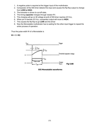
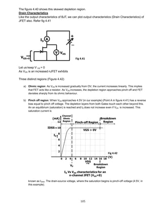
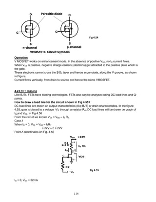
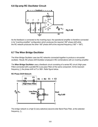
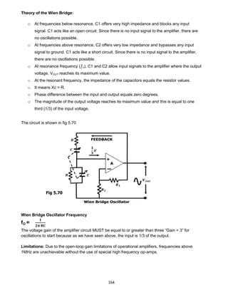
This document describes the basics of analog electronic circuit design, specifically focusing on diodes, transistors, operational amplifiers, and oscillators. It begins by explaining semiconductor theory, including atomic structure, electron and hole dynamics, and the creation of n-type and p-type semiconductors through doping. It then discusses pn junctions, including diffusion, the depletion region, and forward and reverse biasing. The document outlines diode characteristics and applications such as rectifiers and regulators. It also covers bipolar junction transistors, field effect transistors, operational amplifiers, and oscillator circuits. The overall purpose is to address the gap between industry expectations and academic objectives for analog circuit design.


![23
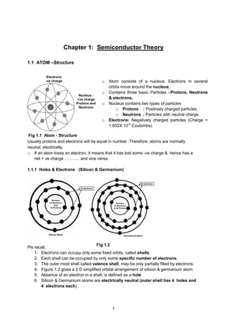
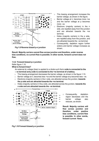
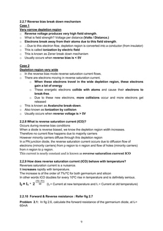
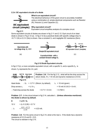
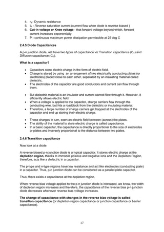
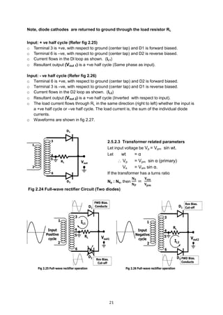
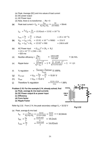
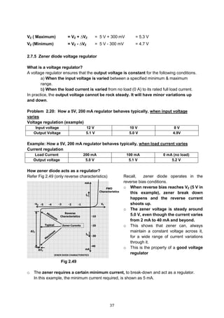
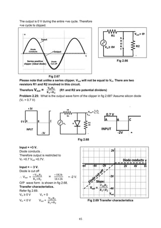
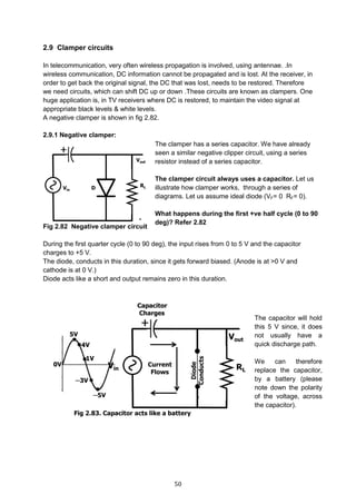
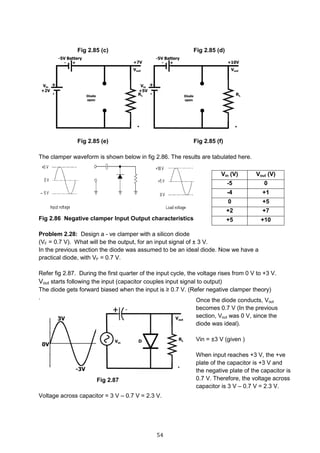
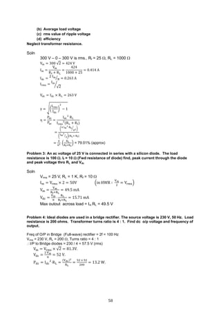
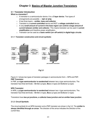
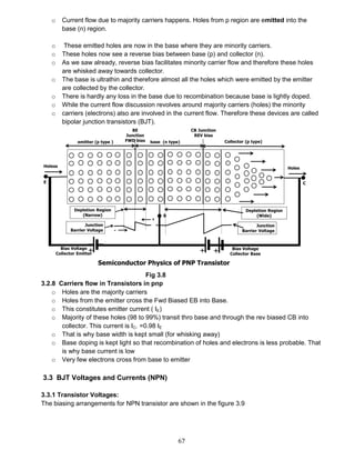
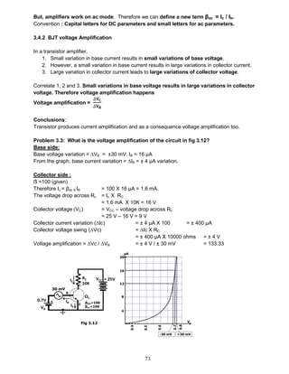
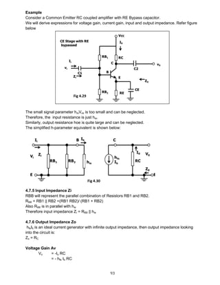
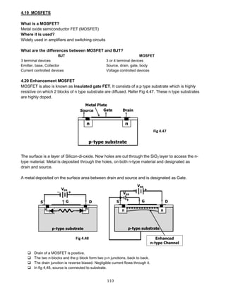
2.5.3 RECTIFIERS EQUATIONS (Refer fig 2.30)
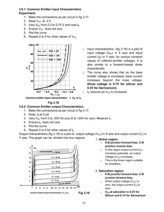
Half wave Full wave
DC Current Idc
Idc =
1
2π
∫ Im sin α dα
π
0
=
Im
2π
[− cos α]0
π
=
−Im
2π
[−1 − 1]
Idc =
Im
π
Idc =
Vm
π (Rf + RL + RS)
DC Current Idc
Idc =
1
π
∫ Im sin α dα
π
0
=
Im
π
[− cos α]0
π
=
−Im
π
[−1 − 1]
Idc =
2Im
π
Idc =
2Vm
π (Rf + RL + RS)
DC output Voltage Vdc
Vdc = IdcRL =
IM
π
RL
=
VM
π (1 +
Rf
RL
)
(Assume RS = 0)
DC output Voltage Vdc
Vdc = IdcRL =
2IM
π
RL
=
2VM
π (1 +
Rf
RL
)
(Assume RS = 0)
Fig 2.30](https://image.slidesharecdn.com/aecdbook-180906093230/85/Analog-Electronic-Circuit-Design-AECD-text-book-30-320.jpg)
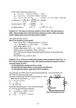
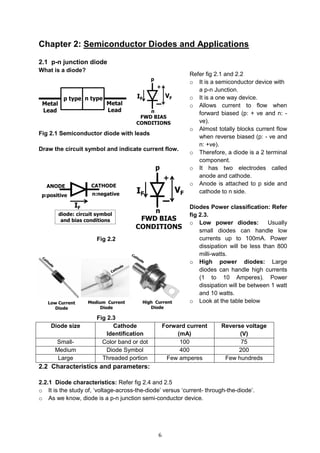
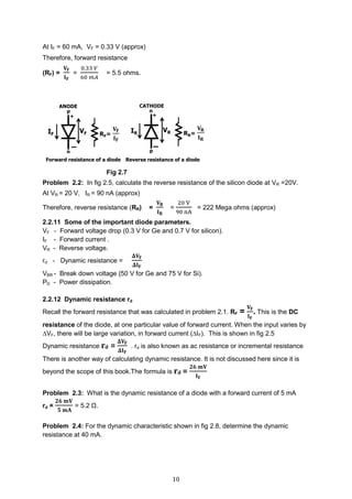
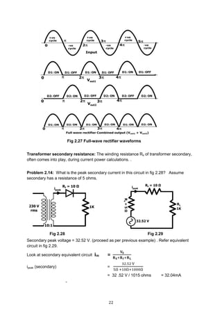
![29
The same bridge rectifier is redrawn to provide more clarity in fig 2.35(a).
+ve cycle:
When the input is a +ve cycle, top of the secondary is +ve and the bottom is –ve.
Diodes D1 and D3 will conduct as shown in fig 2.36.
─ ve Cycle:
When the input is a -ve cycle, bottom of secondary is +ve and the top is –ve.
Diodes D2 and D4 will conduct as shown in fig 2.36(a).
Note, the current through RL, is in the same direction (right to left), in both cycles
Equations of bridge rectifier:
They are same as that of FWR, except Im
Im =
𝐕 𝐦
𝐑 𝐬+𝐑 𝐟+𝐑 𝐟+𝐑 𝐋
[ since, 2 diodes are involved, per cycle]
IDC = 2
𝐈 𝐦
, VDC = 2
𝐕 𝐦
, Irms =
𝐈 𝐦
√𝟐
PDC = (IDC)2
X RL =
𝟒
𝟐
Im
2
RL
Pac = I2
RMS (RS + 2 Rf + RL) =
𝐈 𝐦
𝟐
𝟐
[RS + 2Rf + RL]
Efficiency (η) =
𝟖
𝟐
[ RL / (RS + 2Rf + RL) ] % = 81.2 %
F = 1.11, ϒ = 0.48, TUF = 0.812
2.5.5 Comparison of rectifiers
Compare advantages & disadvantages of all the three rectifiers.
H W F W Bridge
Only one diode. Easy design. 2 diodes. Complex design. 4 diodes. Complex design.
No centre-tap transformer Centre-tap transformer No centre-tap transformer
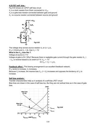
Ripple factor high. (1.21) Ripple factor Low. ( 0.48) Ripple factor low. (0.48)
TUF low. Inefficient. TUF High. Efficient. TUF high. Efficient.](https://image.slidesharecdn.com/aecdbook-180906093230/85/Analog-Electronic-Circuit-Design-AECD-text-book-36-320.jpg)
![31
Irms Im
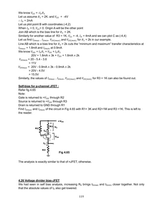
2
Im
√2
Im
√2
Vrms Vm
2
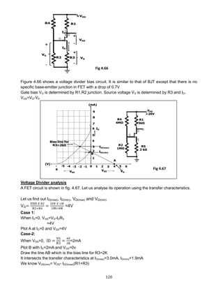
Vm
√2
Vm
√2
PDC - DC Power
output (
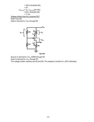
Im
π
)
2
(
2Im
π
)
2
(
2Im
π
)
2
Pac - AC Power
output (
Im
2
)
2
(Rs + Rf + RL) (
Im
√2
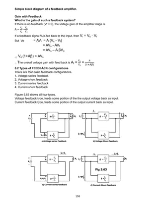
)
2
(Rs + Rf + RL) (
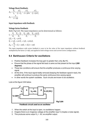
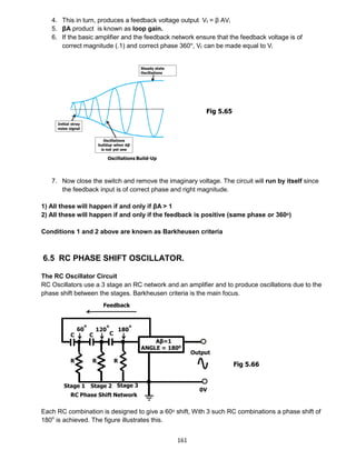
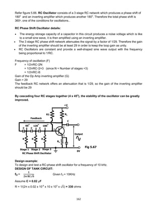
Im
√2
)
2
(Rs + 2Rf + RL)
Efficiency 40.6% 81.2% 81.2%
Form factor 1.57 1.11 1.11
Ripple factor 1.21 0.482 0.482
TUF 0.287 0.812 0.693
Ripple freq f 2f 2f
PIV Vm 2 Vm Vm
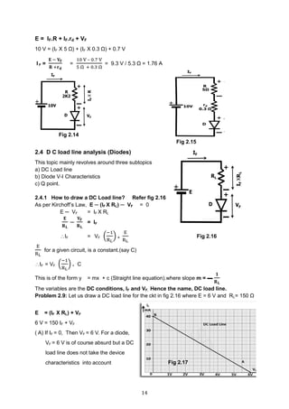
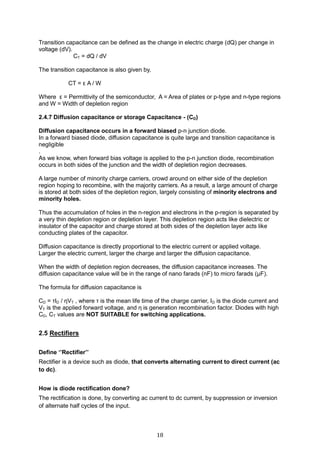
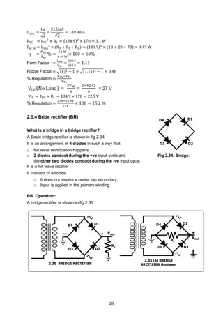
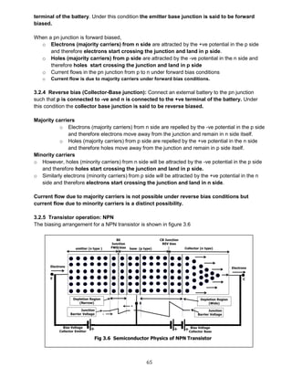
2.6 Capacitor Filter Circuit
2.6.1 Half-wave rectifier with Capacitor filter
Fig 2.37 shows a HW rectifier, with a capacitor filter. Let us assume an ideal diode . VF =0
Operation What happens in cycle 1? 0 to 90 deg (Refer
fig 2.38)
o Input is switched on. During the first
quarter positive cycle (0 to 90 deg) of
the input, the diode conducts and the
capacitor charges to the peak value of
the input .
90 deg to 360 deg [Refer fig 2.38(a)]
o From 90 deg to 360 deg of the first
cycle the diode does not conduct .
Fig 2.37](https://image.slidesharecdn.com/aecdbook-180906093230/85/Analog-Electronic-Circuit-Design-AECD-text-book-38-320.jpg)
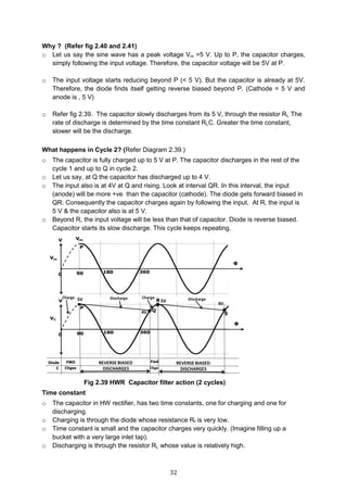
![33
o Time constant is large and the capacitor discharges very slowly. (Imagine emptying the
bucket through a very small outlet tap).
Output ripple will be less as seen above. The ripple factor ϒ, frequency, capacitor value and
the load resistor are inter-related by the equation,
o For a half wave rectifier, ϒ =
𝟏
𝟐√𝟑 𝐂𝐟𝐑 𝐋
2.6.2 Full wave rectifier with capacitor filter
The theory is exactly similar to HW rectifier discussed earlier. The circuit diagram of FWR
and the wave forms are shown in fig 2.40.
Wave forms are shown in fig 2.40(a)
Why capacitor filter? Fig 2.40(a) FWR - Capacitor filter action (2
cycles).
Output ripple will be less as seen above. The ripple factor ϒ, frequency, capacitor value and
the load resistor are inter-related by the equation,
For a full wave rectifier, ϒ =
𝟏
𝟒√𝟑 𝐂𝐟𝐑 𝐋
Problem 2.20: If a full wave rectifier is fed a sine wave of 10 V, 400 Hz, what is the
capacitor value required, if the load current required is 20 mA and ripple factor is 2
%
Full wave rectifier .Ripple = 2f = 800 Hz.
What is RL?
VDC =
𝟐𝐕 𝐦
𝛑
IDC X RL =
𝟐𝐕 𝐦
𝛑
RL =
𝟐𝐕 𝐦
𝛑
X
𝟏
𝐈 𝐃𝐂
Sine wave i/p = 10 V (rms) [unless otherwise mentioned V is rms]
Vm = 10 V X √𝟐 = 14.14 V
IDC = 20 mA
Fig 2.40
Fig 2.40](https://image.slidesharecdn.com/aecdbook-180906093230/85/Analog-Electronic-Circuit-Design-AECD-text-book-40-320.jpg)
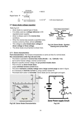
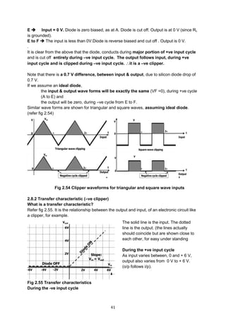
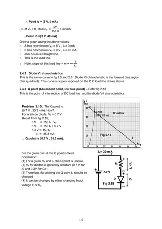
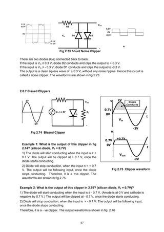
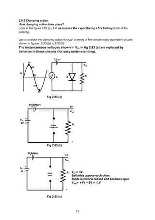
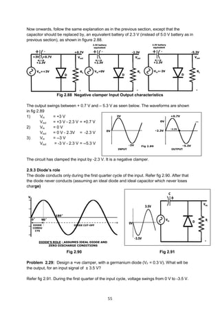
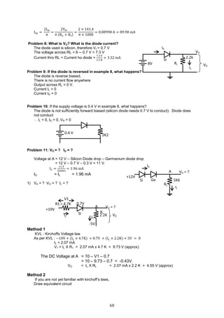
![46
2.8.5 Negative shunt clippers
Refer circuit diagram 2.70. It is similar to parallel +ve clipper, except that the diode is
reversed. Again assume an ideal diode (VF = 0 V, RF = 0 )
Fig 2.70 Negative clipper
Please note that unlike a series clipper, Vout will not be equal to Vin. There are two
resistors R1 and R2 involved in this circuit. The waveforms are shown in fig 2.72
Therefore Vout =
𝐕𝐢𝐧 𝐑 𝟐
𝐑 𝟏+𝐑 𝟐
(R1 and R2 are potential dividers)
Transfer characteristics (fig 2.71)
Fig 2.71 Transfer Characteristics Fig 2.72
Vin ≥ 0 V Vout =
VinR2
R1+R2
Vin < 0 V Vo = 0
2.8.6 Shunt Noise clipper (Using Germanium Diodes)
Refer fig 2,73 for circuit diagram. Assume germanium diodes. (VF = 0.3 V)
Look at input wave form. It has ripples (noise) between + 1.5 V & + 2.0 V and also between
-1.5 V and -2.0 V..
Negative clippers
- ve input cycle
o When Vin < 0 V, the diode is forward biased.
o Diode conducts and forms a short ckt. [Ideal diode
VF = 0 V]
o The output is 0 V during the entire -ve cycle.
o Therefore -ve cycle Is clipped.
+ve input cycle
o When Vin ≥ 0V, the diode is reverse biased.
o The diode is cut off and becomes an open circuit.
o It is as if, the diode is not there at all.
o Therefore Vout follows Vin for the entire –ve cycle.](https://image.slidesharecdn.com/aecdbook-180906093230/85/Analog-Electronic-Circuit-Design-AECD-text-book-53-320.jpg)
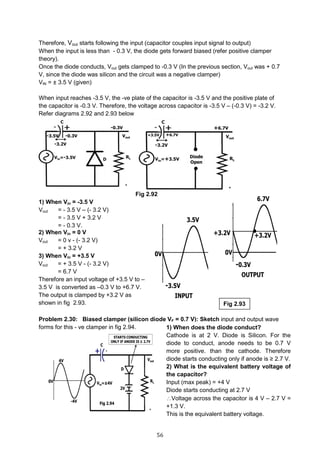
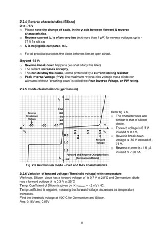
![59
Problem 5: For the circuit shown, fine max and min vale of Zener current.
Case 1
I2 (Max) occurs when
(a) RL is removed and
(b) Vin is maximum
IZMax =
120−50
5K
= 14 mA.
The entire current flows thro Zener since RL is removed
Case 2
I2 (Min) occurs when
(a) 10K is connected (RL)
(b) Vin = Min = 80 V
since Zener voltage = 50 V, voltage across
RL also is 50 V
IL =
50V
10K
= 5 mA.
I1 =
80−50
5K
= 6 mA.
IZ min = I1 – IL = 6 ─ 5 = 1mA
Problem 6: A 24 V, 600 mw Zener diode is used to provide 24 V stabilized supply to a variable
load. Input is 32 V. RL = 1200 .
Calculate
(1) The series resistance required.
(2) Zener current when load = 1200
Soln :
PZ = 600 mw, VZ = 24 V. IZ = ?
(a) PZ = VZ x IZ IZ =
600 mw
24V
= 25 mA
(b) IL =?
24 V
1200
= 20 mA [since Zener voltage = 24 V, voltage across RL also is 24 V]
(c) IS = ? IS = IZ + IL = 25 + 20 = 45 mA
(d) Rs = ? Rs =
Volage across RS
Current thro RS
=
32 V − 24 V
45 mA
=
8 V
45 mA
= 177.78
Problem 7: In a 2 diode full wave rectifier, the voltage across half the secondary is 100 V. Load
Resistance is 950 and Rf = 50 . Find load current of RMS current.
Vrms = 100 V Idc = ? Irms =?
Irms =
Vrms
RL + Rf
=
100
950 + 50
= 100 mA
Vm = Vrms × √2 = 100 × 1.414 = 141.4 V
RL
10K50V
RS
5K80 to
120V
RL = 1200VZ
= 24V
RS = ?
32V
Is
IZ=25mA
IL = ?
10K50V
5K80V
I1
I2
IL
(Min)
5K
50V120V
I2Max](https://image.slidesharecdn.com/aecdbook-180906093230/85/Analog-Electronic-Circuit-Design-AECD-text-book-66-320.jpg)
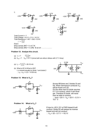
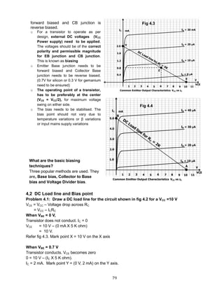
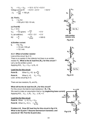
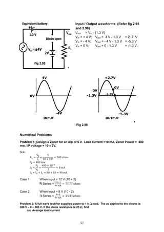
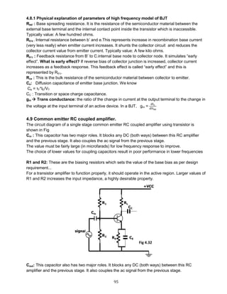
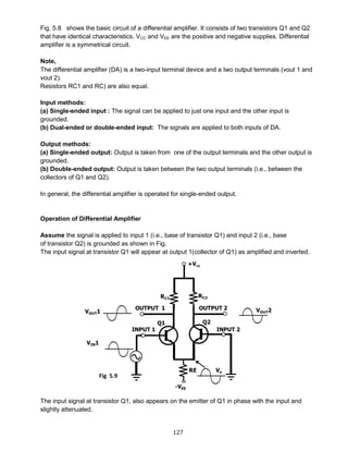
![85
From base side
VCE = IB RB + VBE 4.4.1
IB =
𝐕𝐂𝐂−𝐕 𝐁𝐄
𝐑 𝐁
4.4.2
From collector side
VCE = VCC ─ ( IC + IB ) RC 4.4.3
Self-stabilizing action
Collector to base works in a self-correction mode and has good bias stability.
o If Ic increases for some reason, drop across RC increases
o Therefore VCE drops.
o Because VCE drops, IB decreases.
o Because IB decreases, IC decreases.
Conclusion : If IC tends to increase, the loop prevents this
Tendency
Equating both 4.4.1 and 4.4.3,
IB RB + VBE = VCC - (IC +IB ).RC
Substituting IC = β IB
IB RB + VBE = VCC – [(βIB + IB).RC]
IB RB + [ IB (β + 1) RC ] = VCC ─ VBE
IB =
𝐕𝐂𝐂 ─ 𝐕 𝐁𝐄
𝐑 𝐁 + 𝐑 𝐂 ( 𝛃 + 𝟏 )
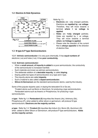
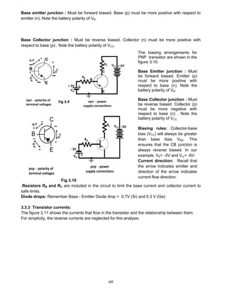
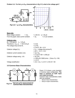
Problem 4.8: For the germanium transistor circuit in fig 4.17,
with collector-to-base bias, determine IB, IC, IE, VCE and Q point.
VBE = 0.3 V (Ger)
IB =
𝐕𝐂𝐂 − 𝐕 𝐁𝐄
𝐑 𝐁 + 𝐑 𝐂( 𝛃 + 𝟏)
=
𝟏𝟐− 𝟎.𝟑 𝐕
𝟐𝟐𝟎𝐊 +𝟐𝐊 (𝟖𝟎 + 𝟏 )
= 31 μA
IC = βIB = 80 X 31 μA = 2.48 mA
IE = IB + IC = 31 μA + 2.48 mA = 2.511 mA (how?)
VCE = VCC - RC (IC + IB)
= 12 V – 2K (2.48 mA + 31 mA)
= 7.0 V.
Q point = ( VCE, IC ) = ( 7.0 V, 228 mA )
Fig 4.16
Fig 4.17
Fig 4.18](https://image.slidesharecdn.com/aecdbook-180906093230/85/Analog-Electronic-Circuit-Design-AECD-text-book-92-320.jpg)
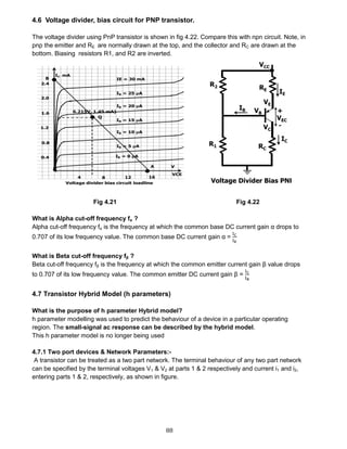
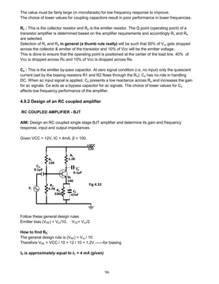
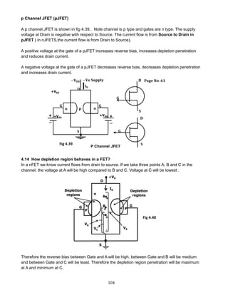
![89
4.7.2 Two port network
Of these four variables V1, V2, i1 and i2, two can be selected as independent variables and the
remaining two can be expressed in terms of these independent variables. This leads to various two
part parameters out of which we will look at H – Parameters (or) Hybrid parameters.
Hybrid parameters (or) h – parameters:-
If the input current i1 and output Voltage V2 are takes as independent variables, the input voltage V1
and output current i2 can be written as
V1 = h11 i1 + h12 V2
i2 = h21 i1 + h22 V2
The four hybrid parameters h11, h12, h21 and h22 are defined as follows.
h11 = [V1 / i1] with V2 = 0
= Input Impedance with output part short circuited (expressed in ohms)
h22 = [i2 / V2] with i1 = 0
= Output admittance with input part open circuited. (expressed in mhos)
h12 = [V1 / V2] with i1 = 0
= reverse voltage transfer ratio with input part open circuited. (No dimensions)
h21 = [i2 / i1] with V2 = 0
= Forward current gain with output part short circuited. (No dimensions)
Necessity of h parameter model
Notations used in transistor circuits:-
hie = h11e = Short circuit input impedance
h0e = h22e = Open circuit output admittance
hre = h12e = Open circuit reverse voltage transfer ratio
hfe = h21e = Short circuit forward current Gain.
4.7.3 The Hybrid Model for Two-port Network:-
V1 = h11 i1 + h12 V2
I2 = h1 i1 + h22 V2
Fig 4.23](https://image.slidesharecdn.com/aecdbook-180906093230/85/Analog-Electronic-Circuit-Design-AECD-text-book-96-320.jpg)
![109
=5000µs X 40mv
=0.2mA
⸫Voltage VD at drain = 𝑉𝐷𝐷 - R1(ID +∆ID)
= 10v-2K(1.5mA+0.2mA)
= 10v-3.4v
= 6.6v
∆VD = 7.0v-6.6v = 0.4v
Variation in drain current at -40mv :∆ID=-0.2mA
⸫Voltage VD at drain = 𝑉𝐷𝐷 - R1(ID −∆ID)
= 10v-2K(1.5mA-0.2mA)
= 10v-2.6v
= 7.4v
∆VD = 7.0v-7.4v = -0.4v
Output variation V0 = ±0.4v
Input variation = ±40mv
⸫Gain of the amplifier= AV =
𝑉𝑜
𝑉𝑖
=
0.4𝑣
40𝑚𝑣
=10
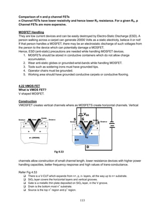
4.18 FET Switch
An FET switch is shown in figure 4,46. It looks similar to a BJT switch.
When the input voltage is zero, FET is on drain current flows. The drain voltage VDS will be at
ground potential. FET in this conduction state has a drain-source on resistance [rDS(on)]. This is very
much lower than the saturation resistance of BJT.
When input goes negative, FET is sufficiently reverse biased so that FET is off and no drain current
flows.VDS=VDD in this state.
You can see when input is ZERO, output is ONE and when input is ONE, output is ZERO. It is an
inverter and a switch.
BJT and FETs have switch on time and off time. These constitute, rise time, fall time and storage
time, popularly termed as propagation delay. Longer the propagation delay, slower is the device.
Which is faster? BJT or FET?
FETs are faster switching devices than BJT since they do not have forward biased junctions
and therefore do not have diffusion capacitance.
Fig 4.46](https://image.slidesharecdn.com/aecdbook-180906093230/85/Analog-Electronic-Circuit-Design-AECD-text-book-116-320.jpg)
![129
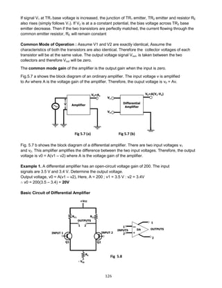
When signal applied to the input of DA produces no phase shift in the output, it is called
noninverting input [See Fig].
In other words, for noninverting input, the output signal is in phase with the input signal. The
noninverting input is then represented by +*sign.
When the signal applied to the input of DA produces 180° phase shift, it is called inverting
input [See Fig].
In other words, for inverting input, the output signal is 180° out of phase with the input
signal.It is often identified with –sign.
Note that in Fig.5.11, the noninverting input terminal is given the +ve sign while the inverting input
terminal is given the –ve sign.
It may be noted that terms noninverting input and inverting input are meaningful when only one
output terminal of DA is available.
Common-mode and Differential-mode Signals
In a differential amplifier, the outputs are proportional to the difference between the two input
signals. Thus the circuit can be used to amplify the difference between the two input signals or
amplify only one input signal simply by grounding the other input.
The input signals to a DA can be of two types.
(i) Common-mode signals (ii) Differential-mode signals
(i) Common-mode signals : When the input signals to a DA are in phase and exactly equal in
amplitude, they are called common-mode signals as shown in Fig 5.12.
The common-mode signals are rejected (not amplified) by the differential amplifier. It is because a
differential amplifier amplifies the difference between the two signals (v1 – v2) and for common-
mode signals, this difference is zero. Note that for common-mode operations, v1 = v2.
(ii) Differential-mode signals. When the input signals to a DA are 180° out of phase and
exactly equal in amplitude, they are called differential-mode signals as shown in Fig 5.12.
The differential-mode signals are amplified by the differential amplifier. It is because the
Fig 5.12](https://image.slidesharecdn.com/aecdbook-180906093230/85/Analog-Electronic-Circuit-Design-AECD-text-book-136-320.jpg)
![132
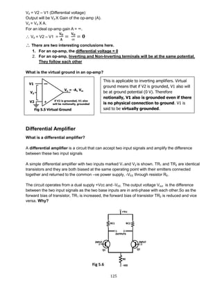
What are the important aspects to be understood, in op amp circuits ?
Note 1: If non- inverting input is grounded, inverting input also will be at ground potential.
This concept is called virtual ground (Inv input will be at ground potential without any physical
connection to ground).
Note 2: If inverting input is at a potential V1, the non – inverting input also be at V1. (“Non-inv”
will follow “inv”).
Note 3: From both (1) and (2), it can be inferred, that inverting and non – inverting inputs follow
each other. The difference between “inv” and “non-inv” inputs is called differential voltage and is
denoted by Vd. (Vd = V+ - V-) Vd in an op-amp is always zero.
Note 4: The current drawn by the inverting input terminal or the non- inverting input terminal
is zero. Therefore, in op amp analysis current drawn by V+ pin or V─ pin can be neglected.
Problem 1: For the op-amp in fig 5.14, the input is a sinewave of I Volt, I kHz. What is the
output?
For non-inverting amplifier, Vout = ─ Vin
𝐑 𝟐
𝐑 𝟏
In this problem, frequency does not matter.
Vin = I Volt. [ I V is rms ( by default ) ]
Vin = I V rms = 1 V X √2 = 1.4 V peak.(just one peak)
= ± 1.4 V peak (both peaks )
Vout = ± 1.4 V X
𝟏𝟎𝟎𝐊
𝟔.𝟖𝐊
= ± 11.8 V peak .
Positive peak is 11.8 V and negative peak is - 11.8 V
This is not possible since the op amp has a DC supply
of +9 V and –9 V. Therefore the peaks will clip at the
power supply voltages.
The input / output waveforms are shown in fig 5.15
Problem 2: What is the input current and load current for
this op-amp shown in fig 5.16?
The inv input terminal is at 0 V (virtual ground ).
Input current =
2 V − 0 V
1K
= 2 mA
Vout = ─ Vin
R2
R1
= ─ 2 X
10K
2K
= ─ 10V](https://image.slidesharecdn.com/aecdbook-180906093230/85/Analog-Electronic-Circuit-Design-AECD-text-book-139-320.jpg)
![134
= 16 X 26 =416 mV
Problem 5: For the circuit in fig 5.20, what is VO? What is the load current?
First, determine the voltage at B. Note the
voltage at B IS NOT 2.2 V but a potential
division of 1K and 1.2 K.
VB =
𝟐.𝟐 𝐕 𝐗 𝟏 𝐊
𝟏𝐊+𝟏.𝟐 𝐊
= 1.0 V
VO = VB (1 +
𝐑 𝐅
𝐑 𝐢𝐧
)
= 1.0 V (1 +
𝟐𝟐 𝐊
𝟐.𝟐 𝐊
)
= 1.0 V X 11 = +11 V. (Non-Inverting)
Problem 6: In the circuit shown in fig 5.21, Vout = ? Vgain =?
Vout = Vin (1+
Rf
Rin
)
What is Vin? Note Vin is NOT 5 V .
It will be the actual voltage Vin at the non-inverting (+)
terminal, after a potential division by R1 and R2.
Vin = 5 V
𝐑𝟐
𝐑𝟏+𝐑𝟐
= 5 V X
𝟑𝟑𝐊
𝟑𝟑𝐊 + 𝟒𝟕𝐊
= 2.1 V
Vout = Vin (1 +
𝐑 𝐟
𝐑 𝐢𝐧
) = 2.1 V (1 +
𝟏𝟎𝟎𝐊
𝟐𝟐𝐊
) = 11.65 V
Vgain =
𝐕 𝐨𝐮𝐭
𝐕𝐢𝐧
=
𝟏𝟏.𝟔𝟓𝐕
𝟓𝐕
= 2.33
5.4 Summing Amplifiers
Non inverting summing amplifier (Refer fig 5.22)
It is a non-inverting amplifier . Therefore Vout = V3 (1 +
𝐑 𝐟
𝐑 𝐢𝐧
)
How to find V3 ?
At the non-inv terminal, I1 flows through R1 and I2 flows through R2,
but the input current Iin to the non- inverting (+) terminal = 0
I1 +I2 = 0
𝐕 𝟏−𝐕 𝟑
𝐑 𝟏
+
𝐕 𝟐−𝐕 𝟑
𝐑 𝟐
= 0
𝐕 𝟏
𝐑 𝟏
+
𝐕 𝟐
𝐑 𝟐
=
𝐕 𝟑
𝐑 𝟏
+
𝐕 𝟑
𝐑 𝟐
= V3 ( 𝟏
𝐑 𝟏
+
𝟏`
𝐑 𝟐
)
𝐕 𝟏 𝐑 𝟐 + 𝐕 𝟐 𝐑 𝟏
𝐑 𝟏 𝐑 𝟐
= V3 ( 𝐑 𝟐 + 𝐑 𝟏
𝐑 𝟏 𝐑 𝟐
)
or V3 =
𝐕 𝟏 𝐑 𝟐 + 𝐕 𝟐 𝐑 𝟏
𝐑 𝟏+ 𝐑 𝟐
Vout = V3 (1 +
𝐑 𝐟
𝐑 𝐢𝐧
) [non–inv op amp ]
= ( 𝐕 𝟏 𝐑 𝟐 + 𝐕 𝟐 𝐑 𝟏
𝐑 𝟏+ 𝐑 𝟐
) (1 +
𝐑 𝐟
𝐑 𝐢𝐧
)
Case 1: Let R1 = R2, then Vout =
𝟏
𝟐
( V1 + V2 ) ( 1 +
𝐑 𝐟
𝐑 𝐢𝐧
)
Fig 5.20
Fig 5.21 Non- Inv
Amplifier
Fig 5.22 Non- Inv
Amplifier](https://image.slidesharecdn.com/aecdbook-180906093230/85/Analog-Electronic-Circuit-Design-AECD-text-book-141-320.jpg)
![135
Case 2: Also let Rf = Rin then Vout = ( V1 + V2 ) [ This is a SUMMING AMPLIFIER ]
Derive an expression for an inverting, summing amplifier.
Refer fig 5.23. VB = 0 VA = 0
I1 + I2 = I
I1 =
𝐕 𝟏 − 𝐕 𝐀
𝐑 𝟏
=
𝐕 𝟏
𝐑 𝟏
( since VA = 0)
I2 =
𝐕 𝟐 − 𝐕 𝐀
𝐑 𝟐
=
𝐕 𝟐
𝐑 𝟐
( since VA = 0)
I =
𝐕 𝐀 − 𝐕 𝐎
𝐑 𝐅
= −
𝐕 𝐎
𝐑 𝐅
I1 + I2 = I
𝐕 𝟏
𝐑 𝟏
+
𝐕 𝟐
𝐑 𝟐
= −
𝐕 𝐎
𝐑 𝐅
VO = - { (
𝐑 𝐅
𝐑 𝟏
) V1 + (
𝐑 𝐅
𝐑 𝟐
) V2 }
Case 1: R1 = R2 = R VO = ─
𝐑 𝐅
𝐑
(V1 + V2) (Summing amplifier)
Case 2: R1 = R2 = RF = R VO = ─ (V1 + V2) (Summing amplifier)
Case 3: R1 = R2 = R and RF = (R/2) Vo = ─
(𝐕 𝟏+𝐕 𝟐)
𝟐
. (Averaging amplifier.)
Problem 7: Refer circuit shown in fig 5.24.
What is the output?
VO = RF (
𝐕 𝟏
𝐑 𝟏
+ 𝐕 𝟐
𝐑 𝟐
+ 𝐕 𝟑
𝐑 𝟑
)
= 12K (
−𝟐 𝐕
𝟐𝐊
+
𝟏.𝟓 𝐕
𝟑𝐊
−
𝟎.𝟓 𝐕
𝟒𝐊
)
= ─ 12 V + 6 V – 1.5 V.
VO = ─ 7.5 V
Summing circuit ( adder ) using super position
Problem 8 : What is the output of this circuit if V1 = 2 V, V2 = 3 V and V3 = 5 V
Refer fig 5.25. This can be analysed by using super position theorem.
Superposition principle : When one voltage source is connected all other voltage source should be
replaced by short. (in this example, to be replaced by ground) .
Fig 5.23 Summing
Amplifier
Fig 5.24
Fig 5.25](https://image.slidesharecdn.com/aecdbook-180906093230/85/Analog-Electronic-Circuit-Design-AECD-text-book-142-320.jpg)
![139
5.6.5 Op-Amp Differentiator: Refer 5.36
Input side output side
I = C
𝐝𝐕𝐒
𝐝𝐭
I =
𝟎−𝐕 𝐨
𝐑 𝐟
C
dVS
dt
=
− 𝐕 𝐨
𝐑 𝐟
Vo = -Rf C
𝐝𝐕𝐒
𝐝𝐭
Therefore Voutput is the differentiation of the input
Applications:
FM demodulators
Signal wave shaping circuits
Problem 11: A sine wave of peak value 6 mv and 2 KHz frequency is applied to an op-amp
integrator. R1= 100K, Cf = 1uF. What is the output voltage?
Solution: For integrator Vo = Vo =
−𝟏
𝐑 𝟏 𝐂 𝐟
∫ 𝐕𝐢𝐧 𝐝𝐭
𝐭
𝟎
where R1 = 100K , Cf = 1uf ,
Vin = Vm Sin(ωt), Vm = 6 mV , ω = 2πf = 2π (2000)
Vo =
−1
100K∗1uf
∫ 6mv ∗ Sin(2π(2000)t) dt
t
0
Vo= - 0.06 [-
𝐜𝐨𝐬(𝟒𝟎𝟎𝟎𝛑𝐭)
𝟒𝛑∗𝟏𝟎𝟎𝟎
]
t
0
Vo = 4.77( cos ( 4000π t ) – 1 ) u volts
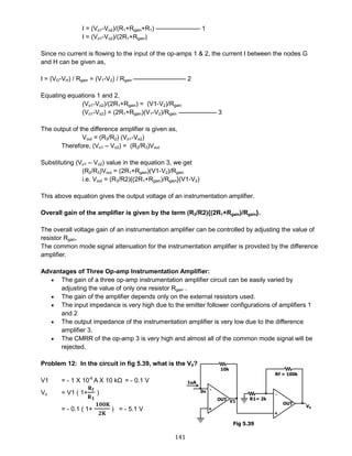
Instrumentation Amplifier
What are the Requirements of a Good Instrumentation Amplifier?
An instrumentation amplifier is used to amplify very low level low-level signals, rejecting noise and
interference signals. Examples can be heartbeats, blood pressure, temperature, earth quakes and
so on
Therefore, the essential characteristics of a good instrumentation amplifier are as follows.
Inputs to the instrumentation amplifiers will have very low signal energy. Therefore the
instrumentation amplifier should have high gain and should be accurate.
The gain should be easily adjustable using a single control.
It must have High Input Impedance and Low Output Impedance to prevent loading.
The Instrumentation amplifier should have High CMRR since the transducer output will usually
contain common mode signals such as noise, when transmitted over long wires.
It must also have a High Slew Rate to handle sharp rise times of events and provide maximum
undistorted output voltage swing
INPUT OUT PUT
COS - SIN
Triangular wave Square wave
Fig 5.36](https://image.slidesharecdn.com/aecdbook-180906093230/85/Analog-Electronic-Circuit-Design-AECD-text-book-146-320.jpg)
![142
Problem 13: In the circuit in fig 5.40, If RL varies from
1k to 60 k. What is the variation in Vo?
1) RL = 1K then Vo = 10 ( -
𝟏𝐊
𝟏𝟎𝟎𝐊
) = - 0.1 V
2) RL = 60K then Vo = 10 ( -
𝟔𝟎𝐊
𝟏𝟎𝟎𝐊
) = - 6.0 V
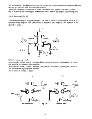
5.7 Differential mode and common mode signals:
Preamble: Input to an op-amp, in general, will have two types of signals called, difference signals
and common mode signals.
Difference signals are those signals present at V1 and V2 which are different (not same).
Common mode signals are those signals present at V1 and V2 which are exactly same.
What is the differential gain ( Ad) ?
Refer fig 5.41
Vd = V1 – V2 (V1 and V2 are different)
Vo = Ad Vd = Ad ( V1 – V2 )
Where Ad = differential gain
and Vd = differential voltage
What is a common mode signal ?
Refer fig 5.42. In common mode V1 and V2 are exactly same. Average level of the two input
signal V1 and V2 is defined as the common mode signal
Vc =
𝐕𝟏 + 𝐕𝟐
𝟐
For a common mode signal also, the op-amp
gives an output V0 = Ac Vc
where Ac = common mode gain
Vc = common mode signal
Therefore the total output of an Op-amp
Vo = common mode output + differential mode output
= AcVc + AdVd
In an ideal op amp
a) Common mode gain Ac must be Zero
b) Differential mode gain Ad must be infinity
What is common mode rejection ratio (CMRR)?
CMRR is the ability of an op-amp to accept the desired differential signals and reject undesired
common mode signals
CMRR = = |
𝐀 𝐝
𝐀 𝐜
|
for ideal op amp CMRR = ∞ [ since Ad = ∞ and Ac = 0 ]
Fig 5.40
Fig 5.41
Fig 5.42](https://image.slidesharecdn.com/aecdbook-180906093230/85/Analog-Electronic-Circuit-Design-AECD-text-book-149-320.jpg)


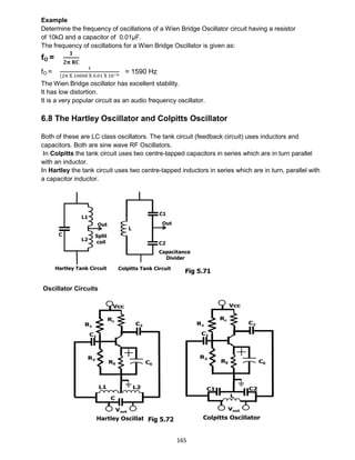
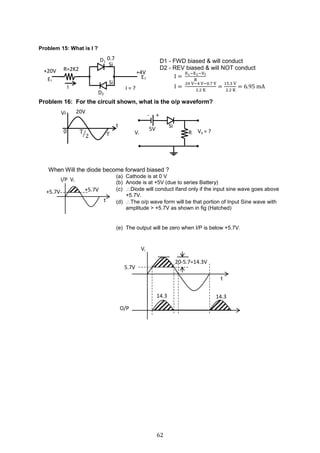
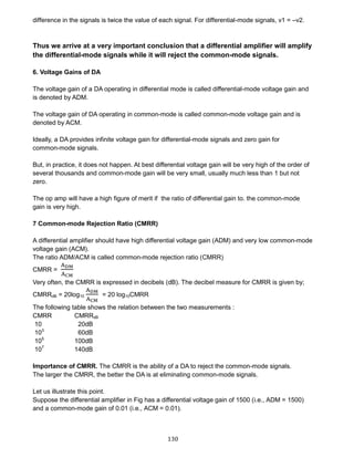
![166
DESIGN:
BJT- Amplifier: Design a typical RC-Coupled BJT Amplifier. A minimum gain of 2.9 is
required to start oscillations.
Design of a Hartley Oscillator for 100 KHz.
fo = 100 kHz
Frequency of oscillation for Hartley Oscillator is given by:
fo =
𝟏
𝟐𝛑√𝑳𝑪
where L= L1 + L2 and [L1< L2]
C =
𝟏
𝟒𝝅 𝟐 𝒇 𝟐 𝐋
Let L1=100 μH, L2=1mH
Therefore, C=2.3nF
Design of a Colpitts Oscillator for 100 KHz.
fo =
𝟏
𝟐𝛑√𝑳𝑪
where Ceff= (C1 C2) /(C1 + C2)
L =
𝟏
𝟒𝝅 𝟐 𝒇 𝟐 𝑪 𝒆𝒇𝒇
Let C1 = C2 =0.01 pF
Therefore L = 0.05066H
Colpitts Oscillator Op-amp Circuit
Colpitts Oscillator sinewaves are purer than Hartley oscillator’s.
Colpitts oscillator can operate at very high frequencies.
Fig 5.73](https://image.slidesharecdn.com/aecdbook-180906093230/85/Analog-Electronic-Circuit-Design-AECD-text-book-173-320.jpg)