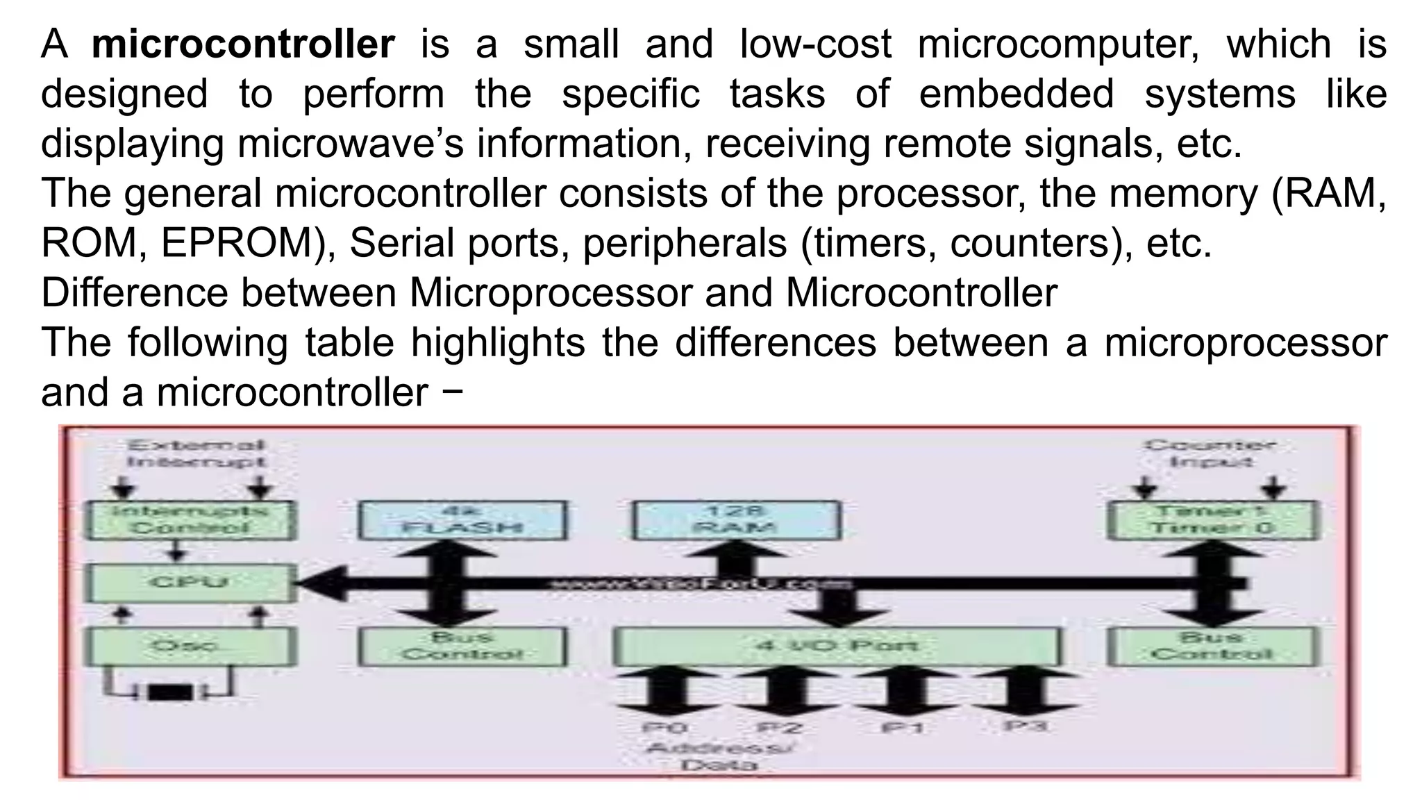
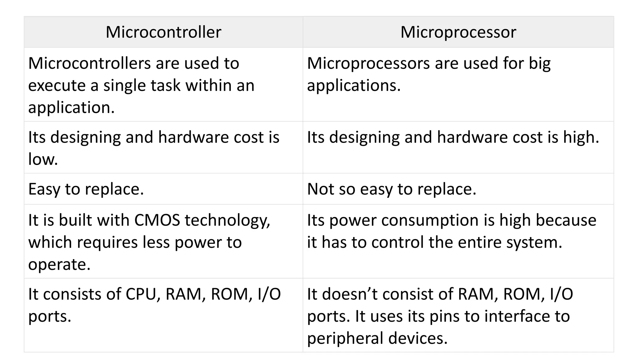
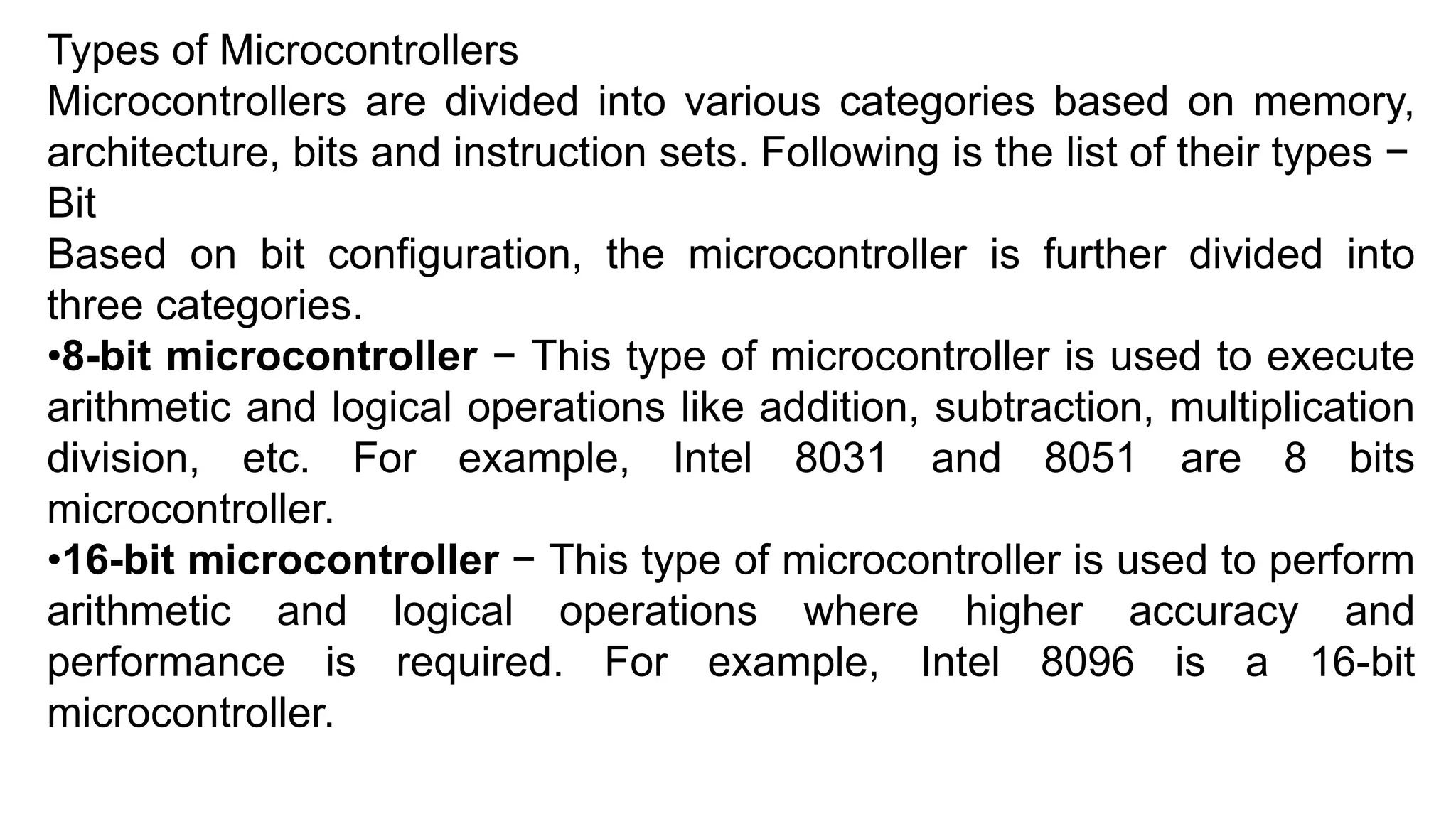
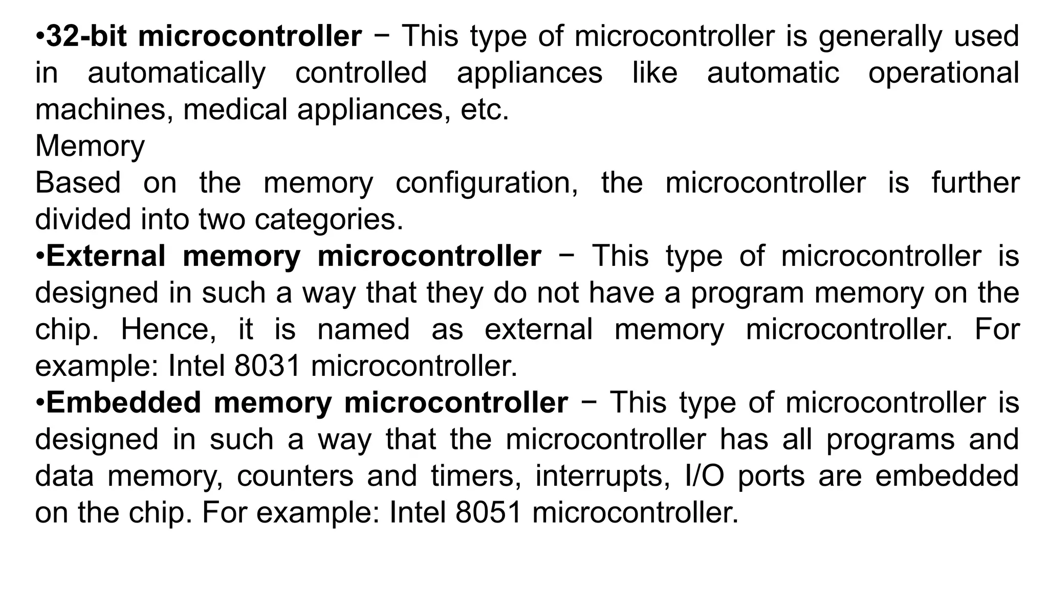
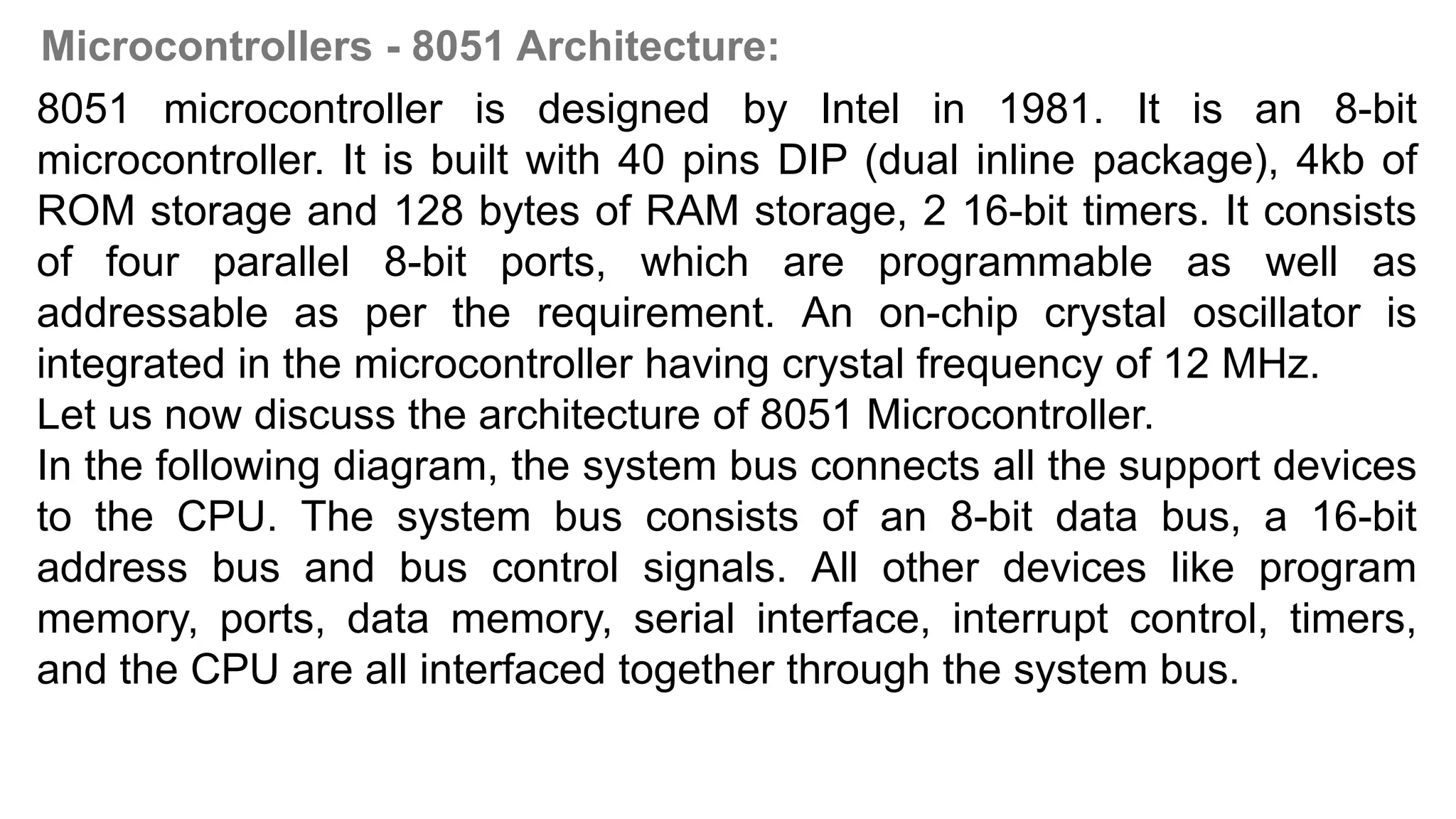
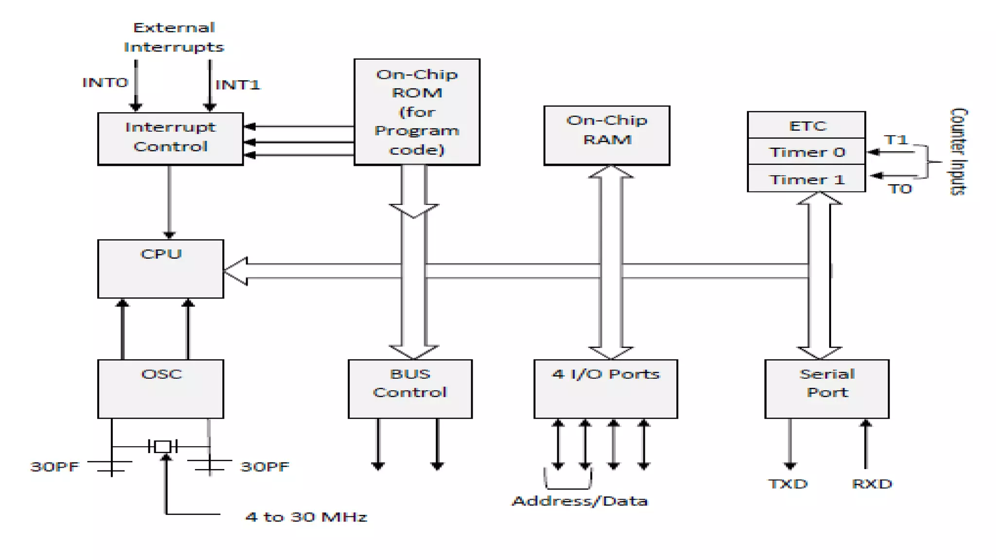
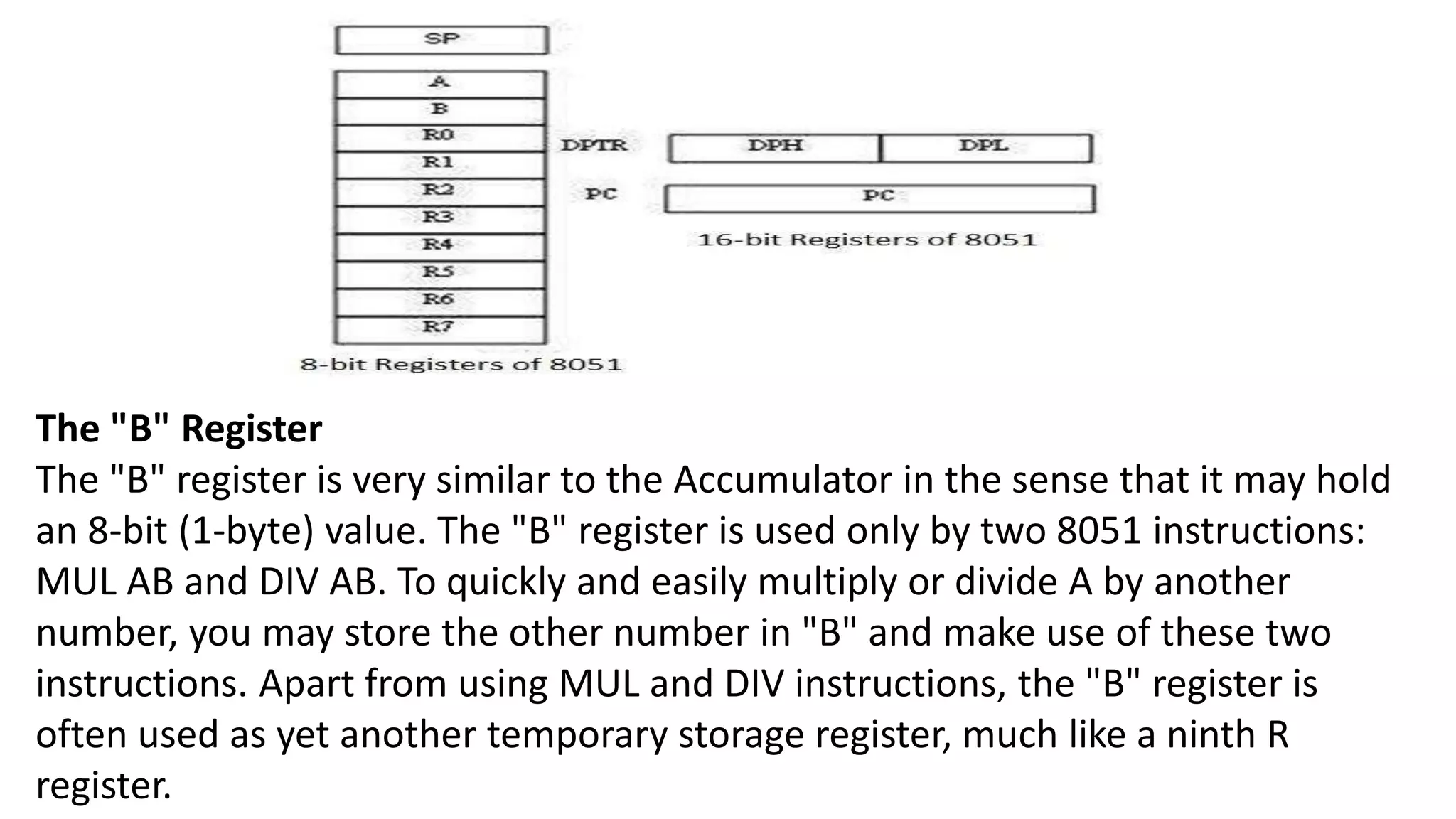
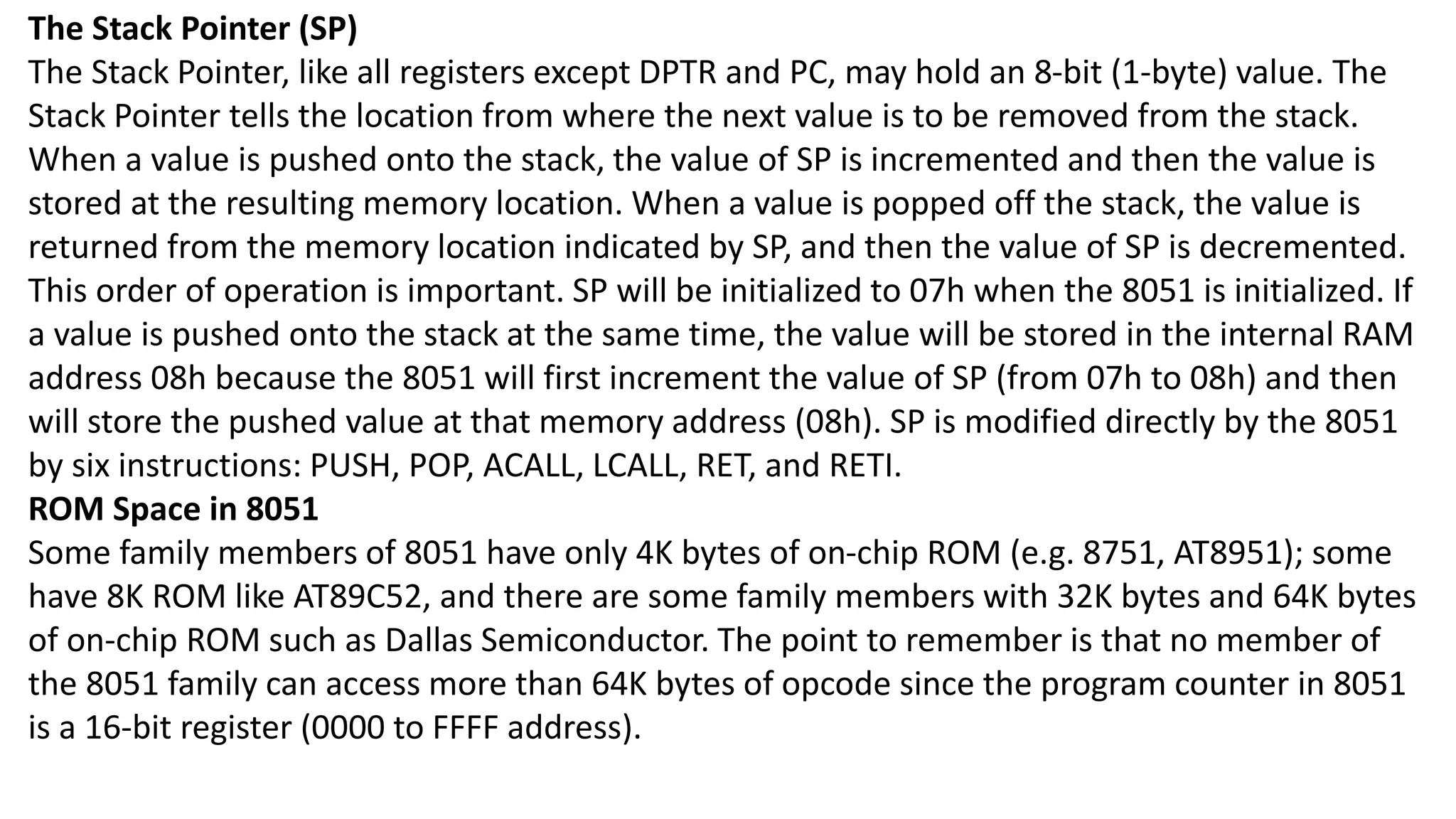
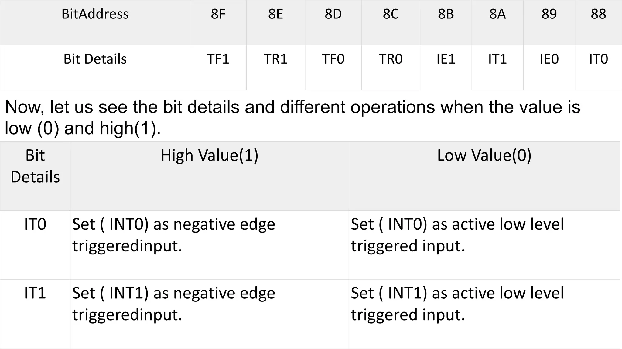
The document discusses the 8051 microcontroller. It was introduced by Intel in 1981 as an 8-bit microcontroller with features like 128 bytes of RAM, 4K bytes of ROM, timers, ports, and peripherals integrated onto a single chip. This led to variants like the 8052 with more RAM and an extra timer. The 8031 has no on-chip ROM. Microcontrollers are used in embedded systems for tasks like displaying microwave information or receiving remote signals. They have lower costs and power usage than microprocessors. The 8051 architecture includes registers like the accumulator, R registers, B register, data pointer, and program counter to interface with memory, ports and peripherals via a system bus.
![Stack in the 8051
As the stack is a section of a RAM, there are registers inside the CPU to point to it. The register
used to access the stack is known as the stack pointer register. The stack pointer in the 8051 is
8-bits wide, and it can take a value of 00 to FFH. When the 8051 is initialized, the SP register
contains the value 07H. This means that the RAM location 08 is the first location used for the
stack. The storing operation of a CPU register in the stack is known as a PUSH, and getting the
contents from the stack back into a CPU register is called a POP.
"PUSH 1" pushes register R1 onto the stack.
Popping the contents of the stack back into a given register
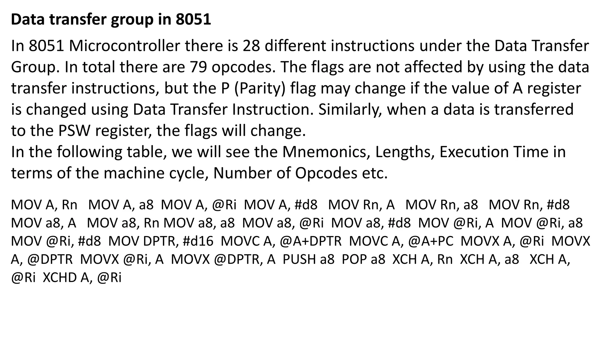
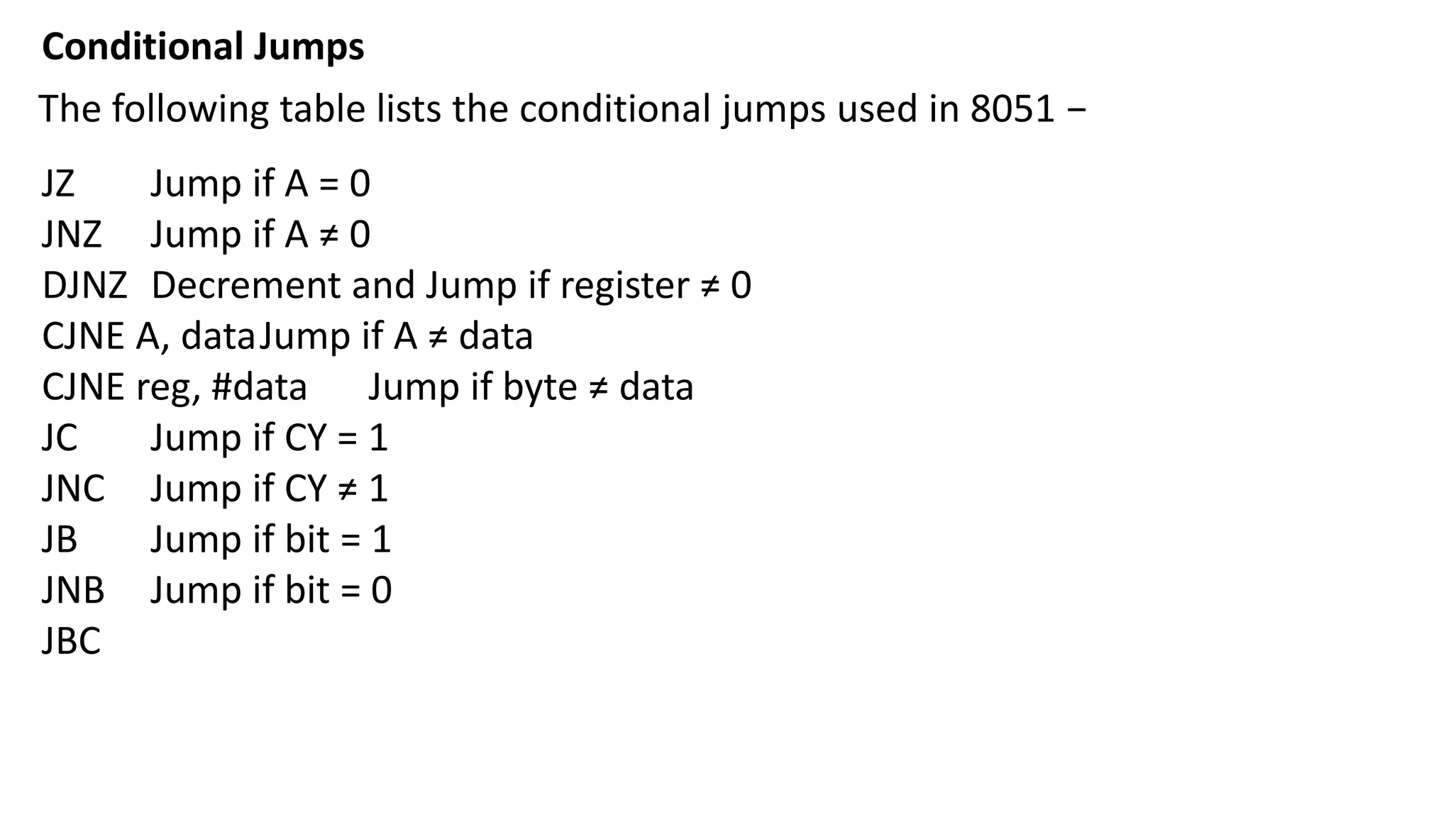
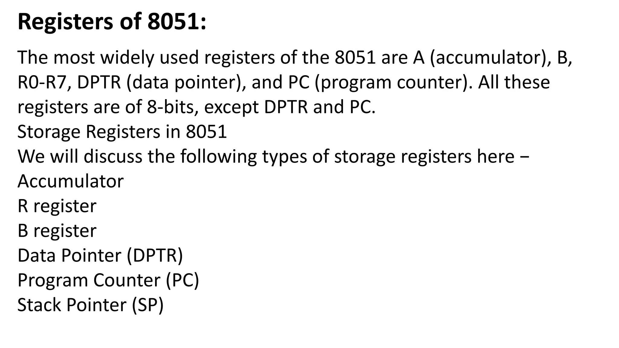
8051 DATA TYPES AND DIRECTIVES:
Microcontroller 8051 has only one 8-bits data type and the size of each register is also 8 bits.
The job of the programmer is to break down data larger than 8 bits [00 to FFH, or 0 to 255 in
decimal] to be processed by the CPU. The data type used by the 8051 can be positive or
negative.](https://image.slidesharecdn.com/bsce5-210129073745/75/B-sc-e5-2-mp-unit-4-mc-8051-21-2048.jpg)
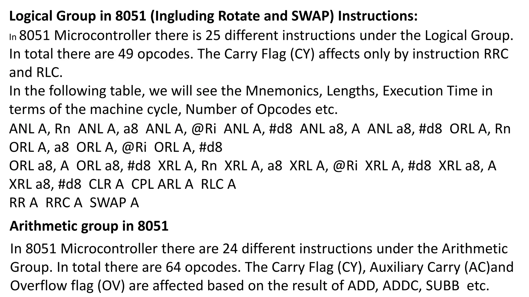
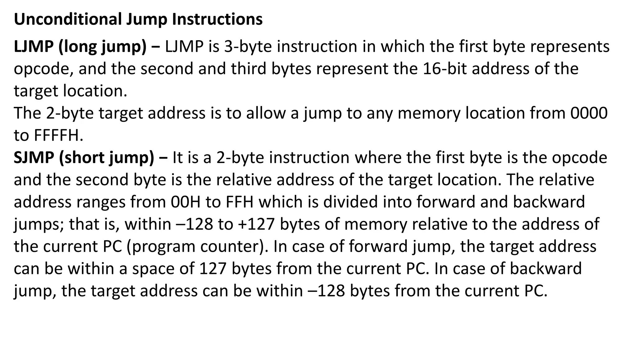
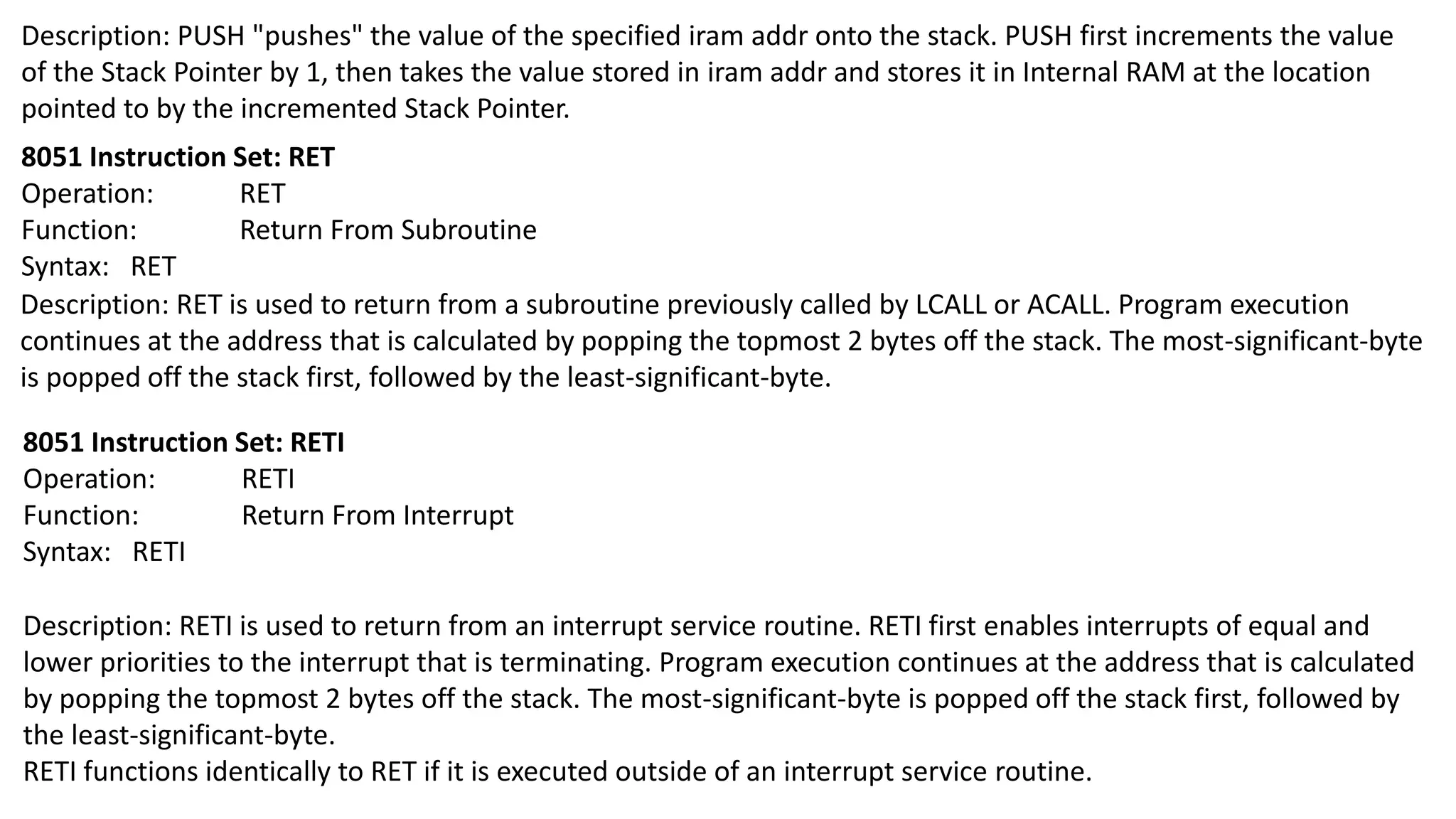
![DB [Define Byte]:
The DB directive is used to define the 8-bit data and the numbers can be in decimal,binary,
hex or ASCII formats. For decimal, the "D" after the decimal number is optional, but using "B"
[binary] and "H" [hexadecimal] is required. The assembler will convert the numbers in hex. To
indicate ASCII, simply put it in quotation marks 'like this'. The assembler will assign the ASCII
code for the numbers or characters automatically. The DB directive is the only directive that
can be used to define ASCII strings larger than two characters. It should be used for all ASCII
data definitions.
Either single or double quotes can be used around ASCII strings. Can be useful for strings,
which contain a single quote such as "O'Really". DB is also used to allocate memory in byte-
sized chunks.
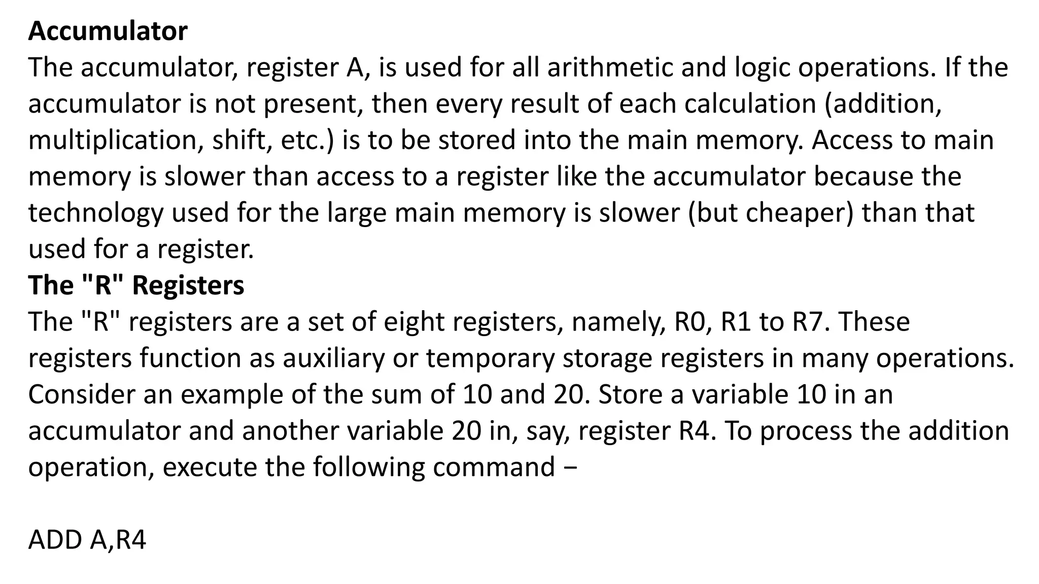
Assembler Directives:
The following Assembler directives are widely used in 8051 Assembly language programming.
ORG [Origin]:
The ORG directive is used to indicate the beginning of the address. The number that comes
after ORG can be either in HEX or in decimal. If the number is not followed by 'H', it is decimal
and the assembler will convert it into hex. Some assemblers use ".ORG" [notice the dot]
instead of "ORG" for the origin directive. For tha you need to check your assembler.](https://image.slidesharecdn.com/bsce5-210129073745/75/B-sc-e5-2-mp-unit-4-mc-8051-22-2048.jpg)
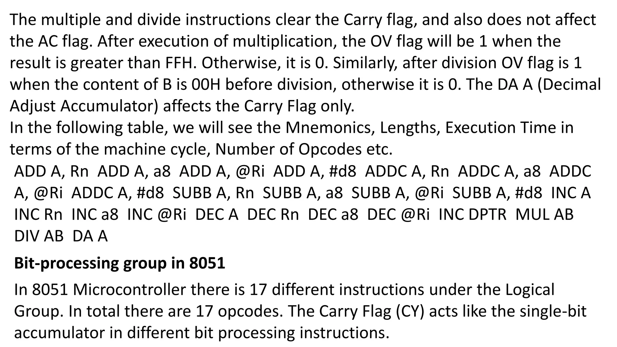
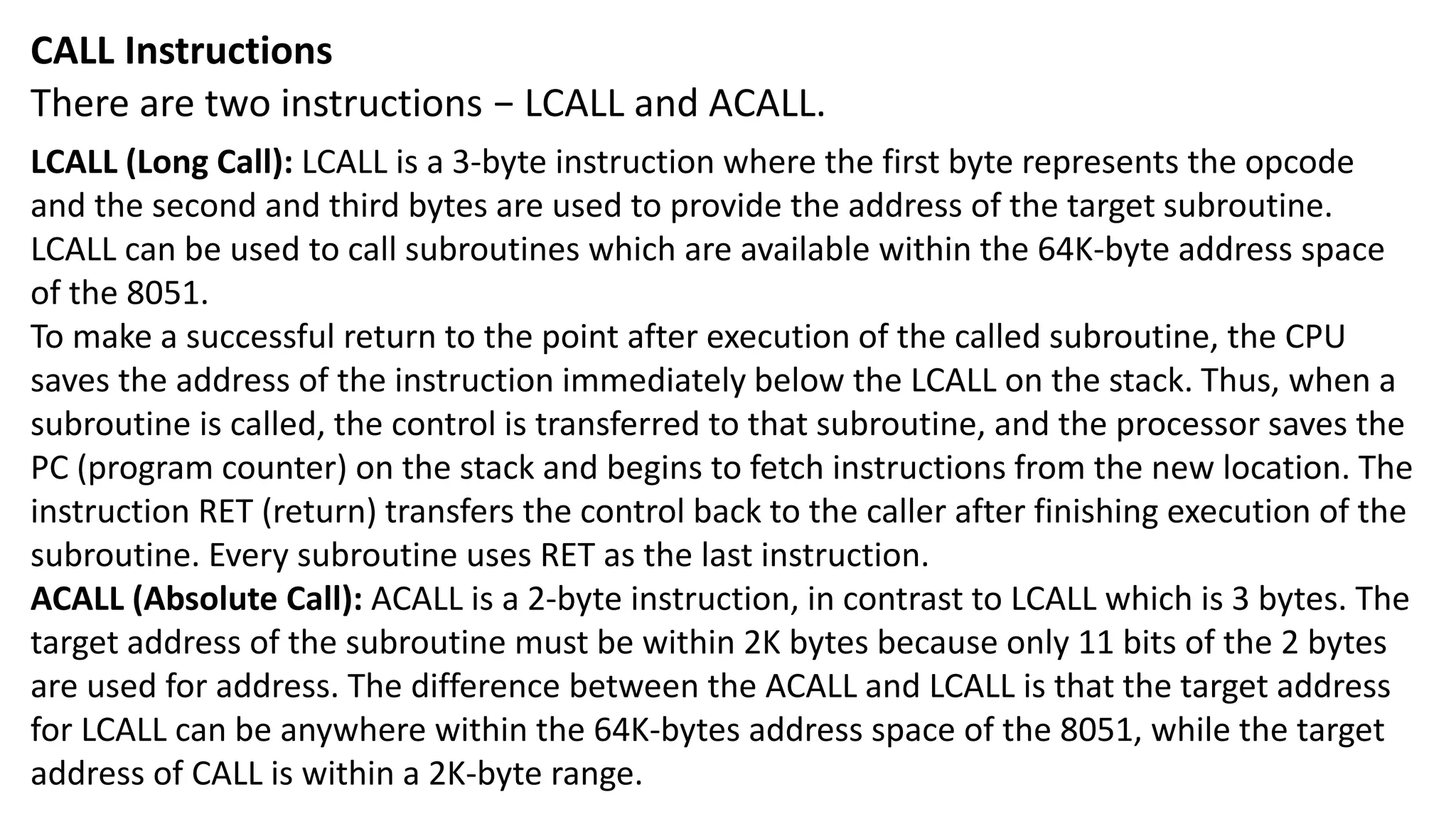
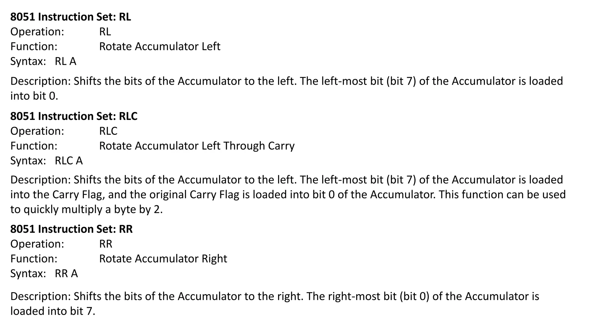
![EQU [Equate]:
EQU is used to define a constant without occupying a memory location. The EQU directive does
not set aside storage for a data item but associates a constant value with a data label so that
when the label appears in the program, its constant value will be substituted for the label. Here
uses EQU for the counter constant ans then the constant is used to load the R4 register.
After executing the instruction "MOV R4,#COUNT", the register R4 will be loaded with the
value 22 [# sign indicates it is a value, notice it].
What is the advantage of using EQU?
The answer is that, lets say in a program there is a constant value [a fixed value] used in many
different places in the program, and the programmer wants to change its value through out
the entire program. By the use of EQU, a programmer can change all valves at once and the
assembler will change all of it occurrences, rather than search the entire program and to
change the value one by one to fine every occurrence, just change the constant value
followed by EQU results changing the all occurrences at once.
END Directive:
END directive pseudocode is very important. END indicates to the assemblere the end of the source [asm ] file.
The END directive is the last line of an 8051 program. In assembly language programming anything after the
END directive is ignored by the assembler. Some assembler uses ".END" [notice the dot] instead of "END"](https://image.slidesharecdn.com/bsce5-210129073745/75/B-sc-e5-2-mp-unit-4-mc-8051-23-2048.jpg)
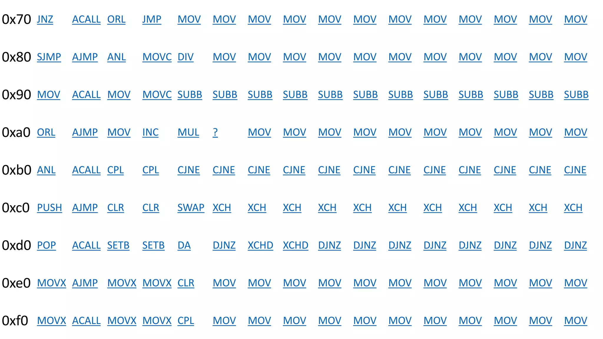
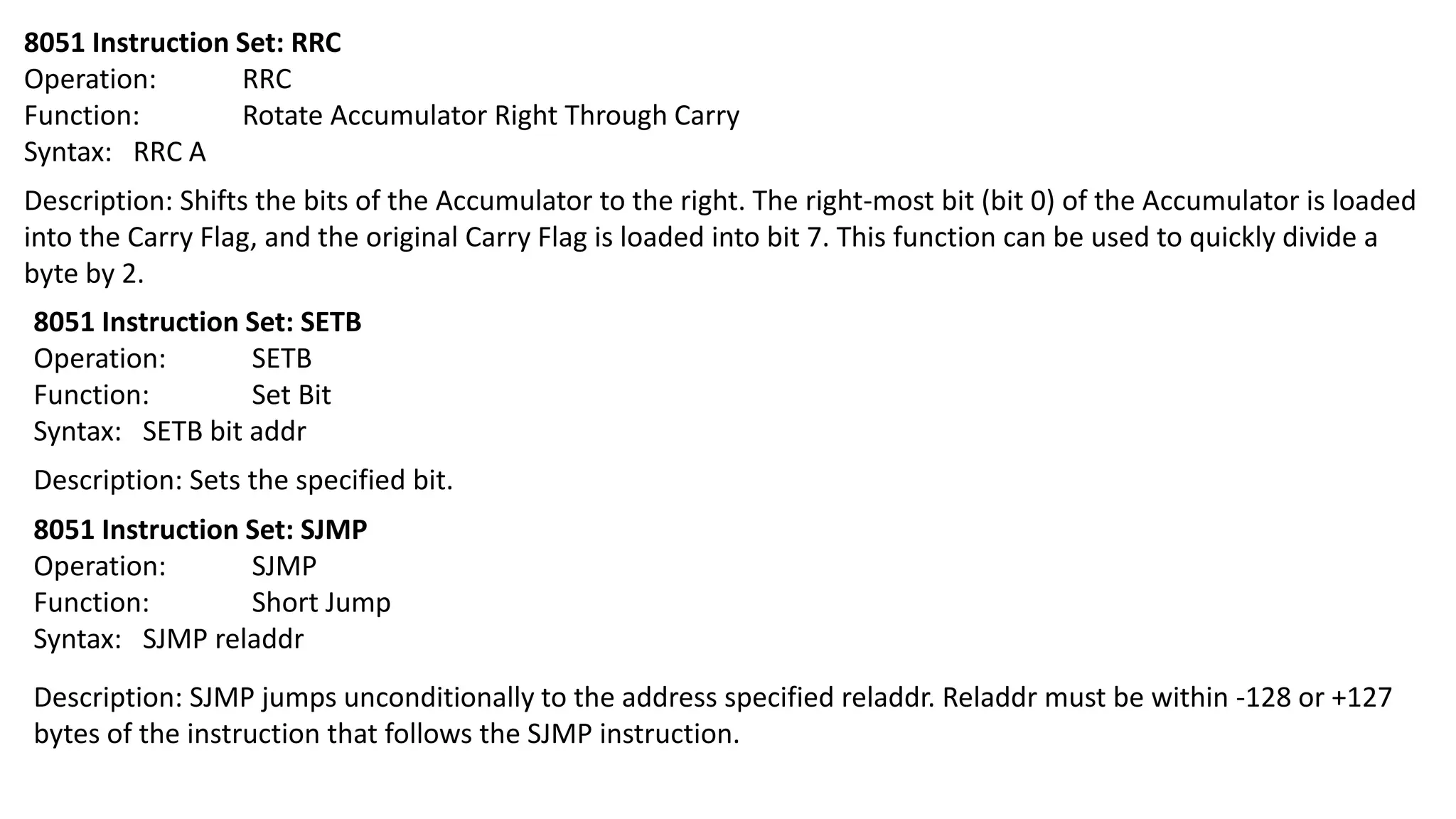
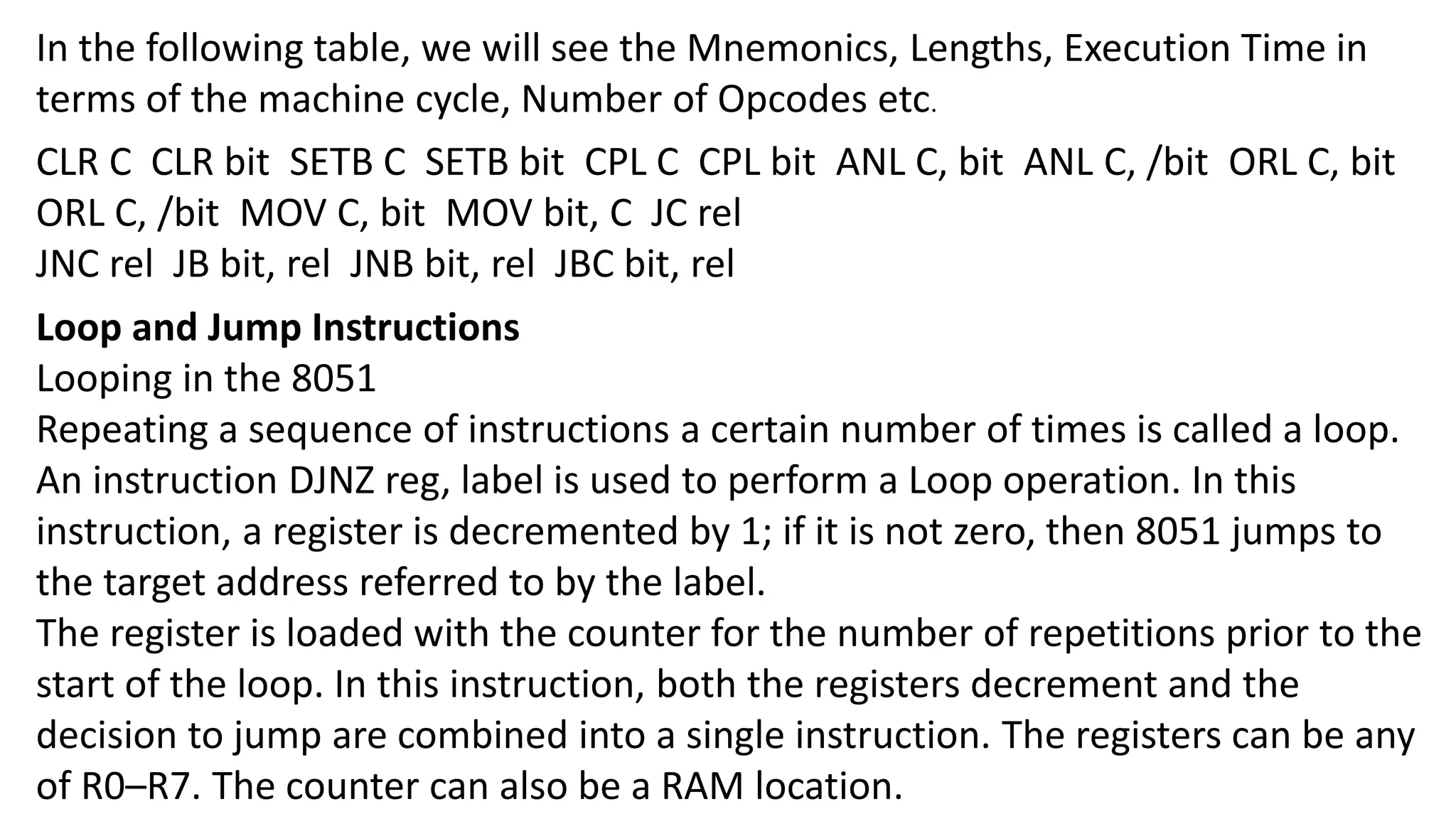
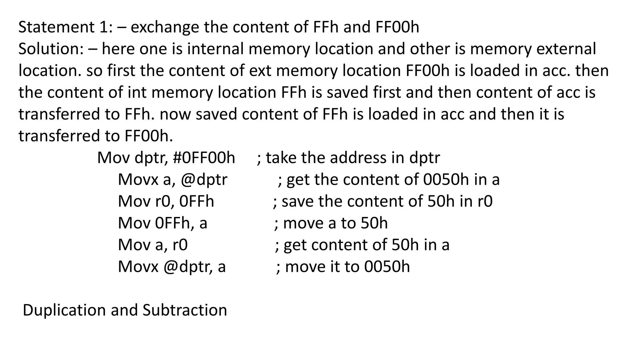
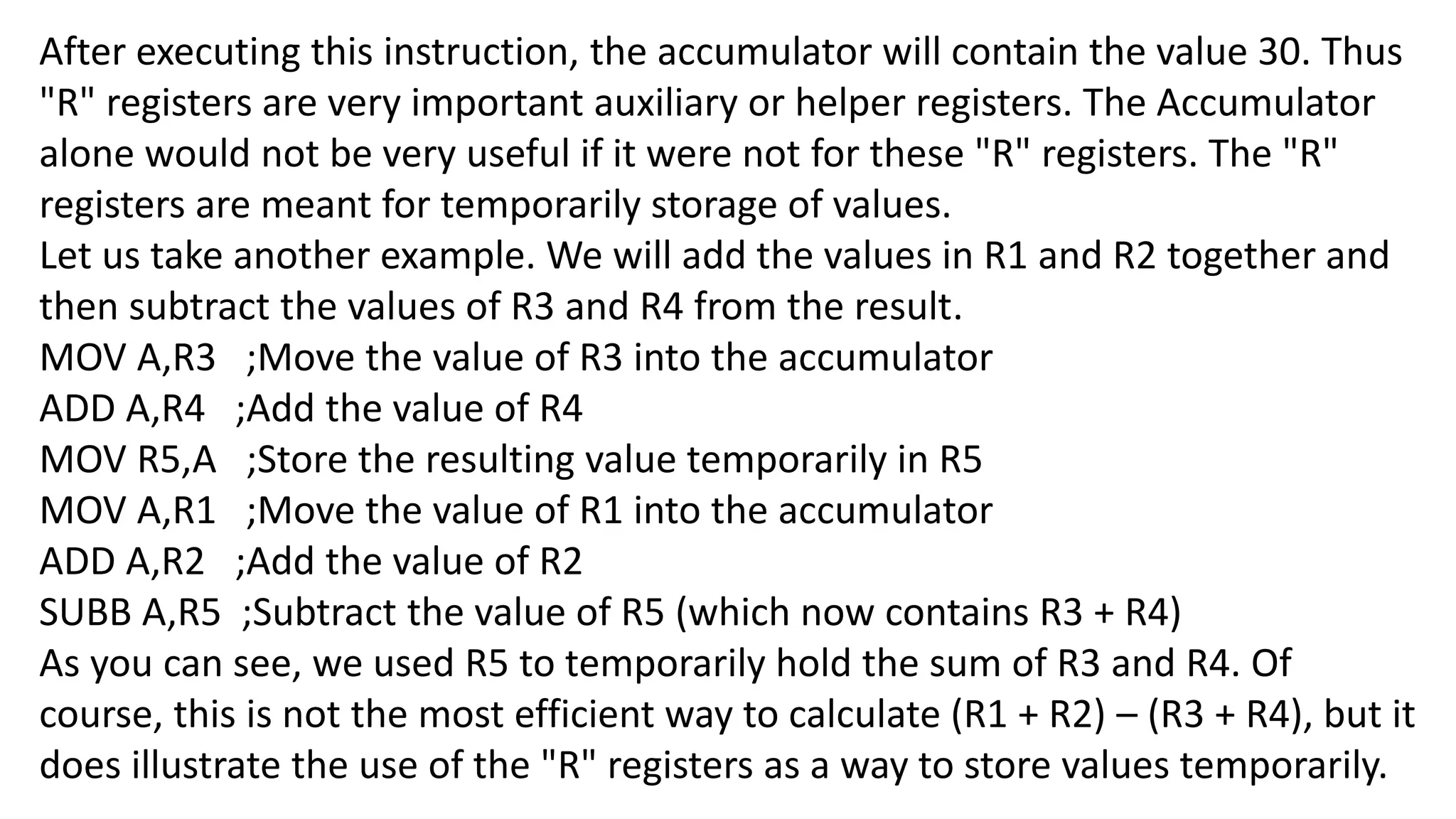
![8051 Instruction Set: XCHD
Operation: XCHD
Function: Exchange Digit
Syntax: XCHD A,[@R0/@R1]
Description: Exchanges bits 0-3 of the Accumulator with bits 0-3 of the Internal RAM address pointed to indirectly
by R0 or R1. Bits 4-7 of each register are unaffected.
8051 Instruction Set: XRL
Operation: XRL
Function: Bitwise Exclusive OR
Syntax: XRL operand1,operand2
Description: XRL does a bitwise "EXCLUSIVE OR" operation between operand1 and operand2, leaving the
resulting value in operand1. The value of operand2 is not affected. A logical "EXCLUSIVE OR" compares the bits of
each operand and sets the corresponding bit in the resulting byte if the bit was set in either (but not both) of the
original operands, otherwise the bit is cleared.](https://image.slidesharecdn.com/bsce5-210129073745/75/B-sc-e5-2-mp-unit-4-mc-8051-82-2048.jpg)