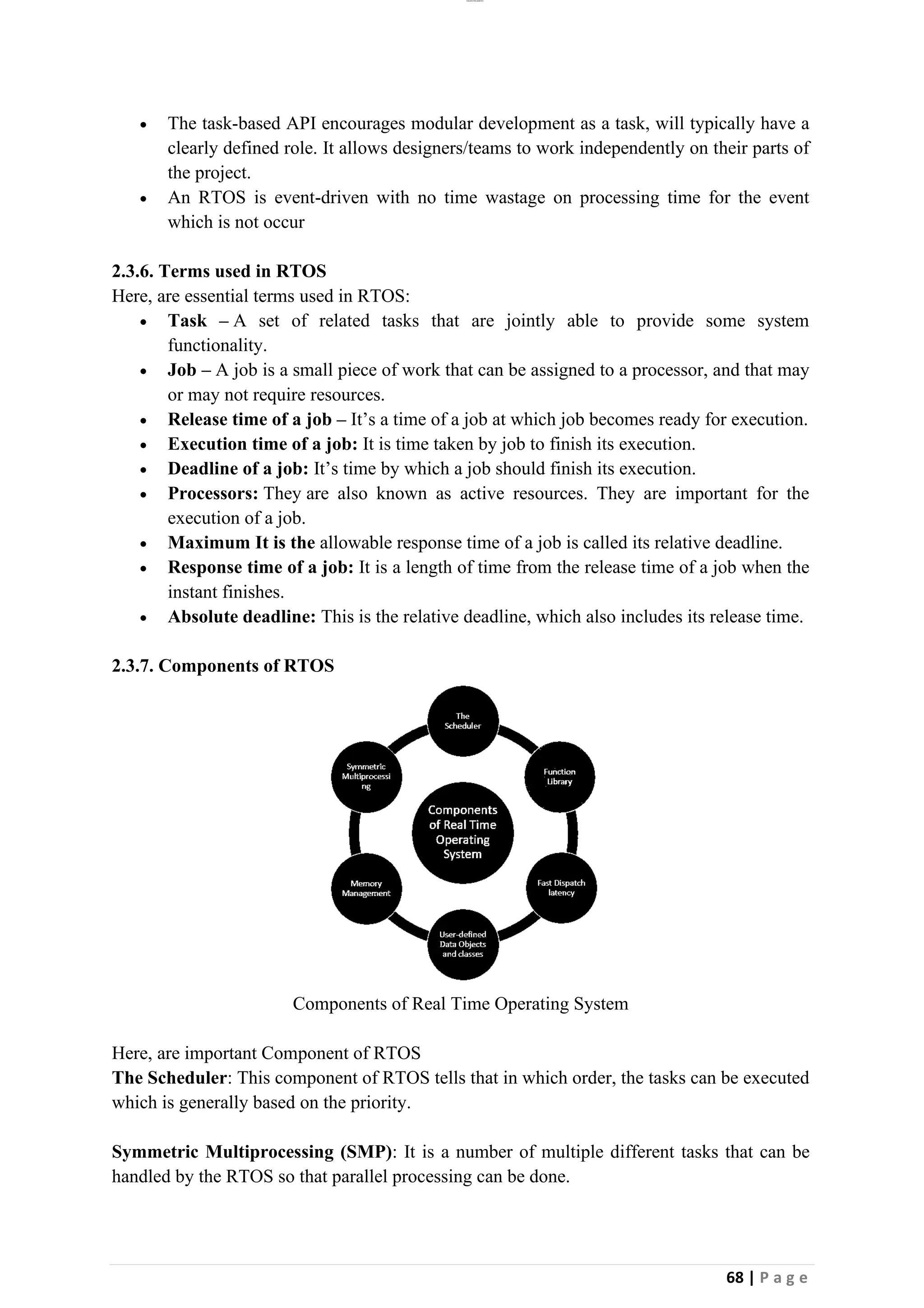
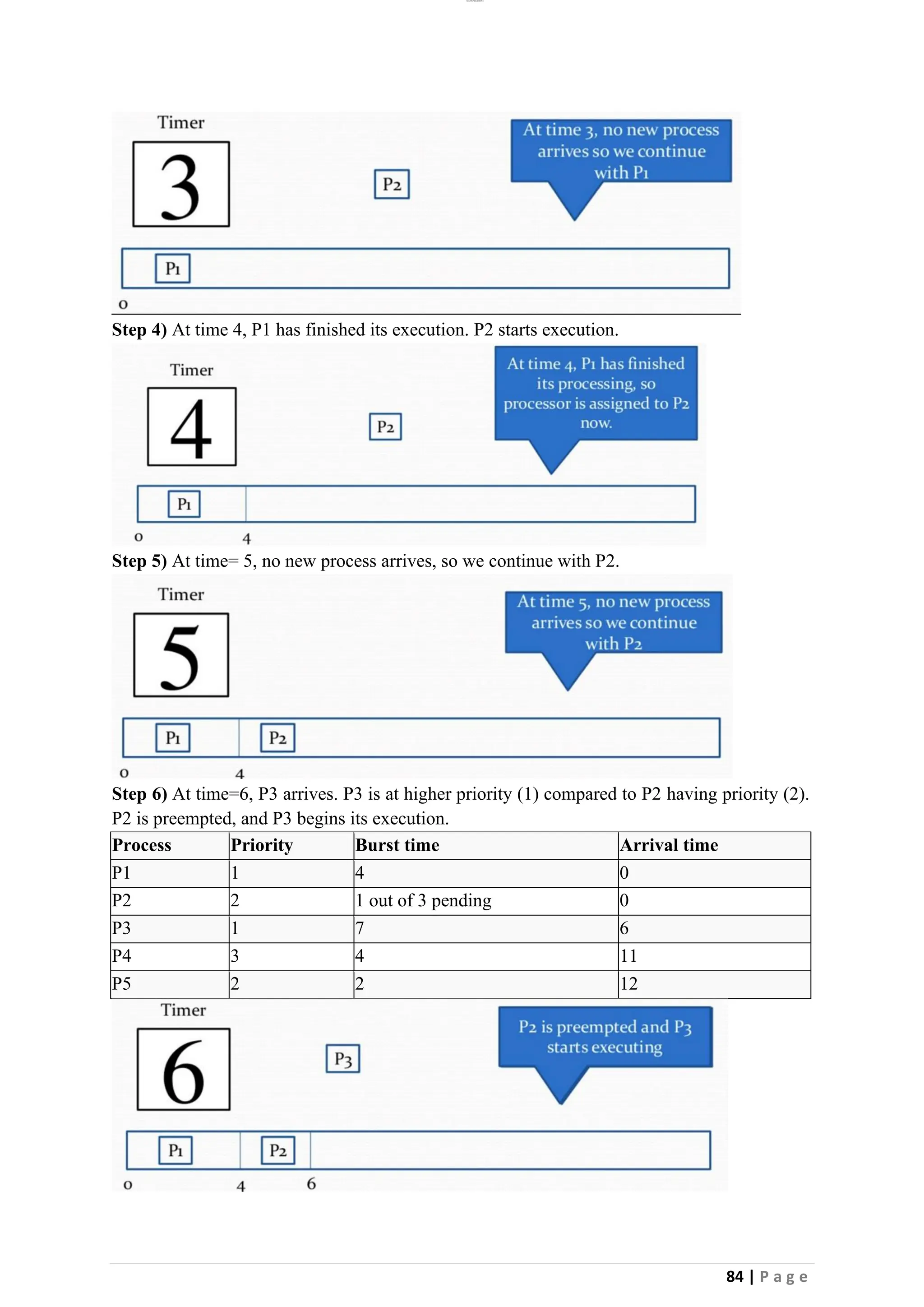
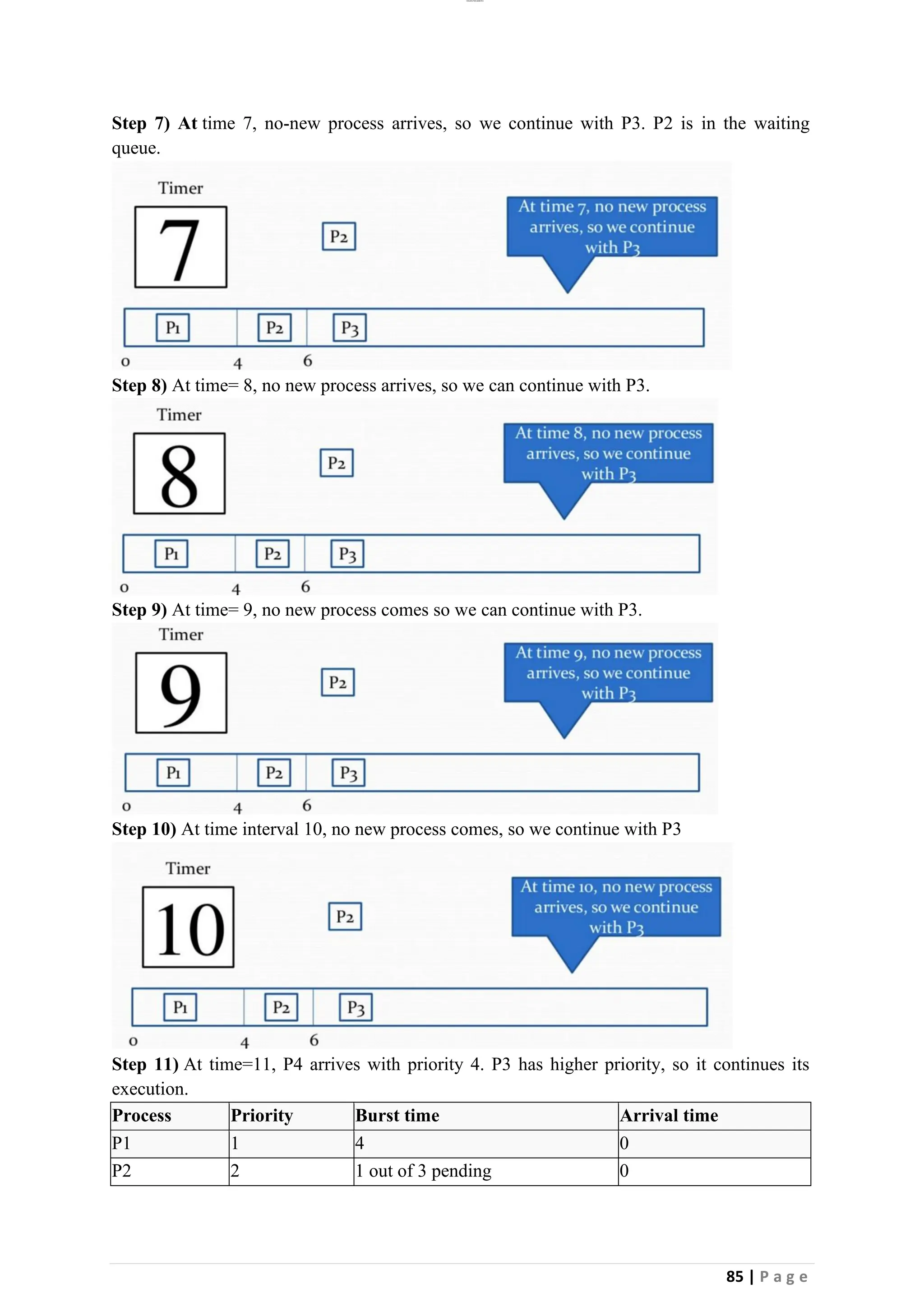
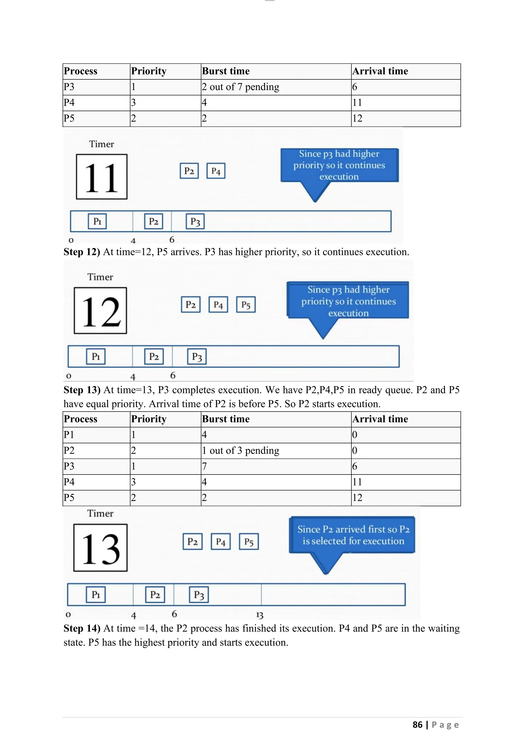
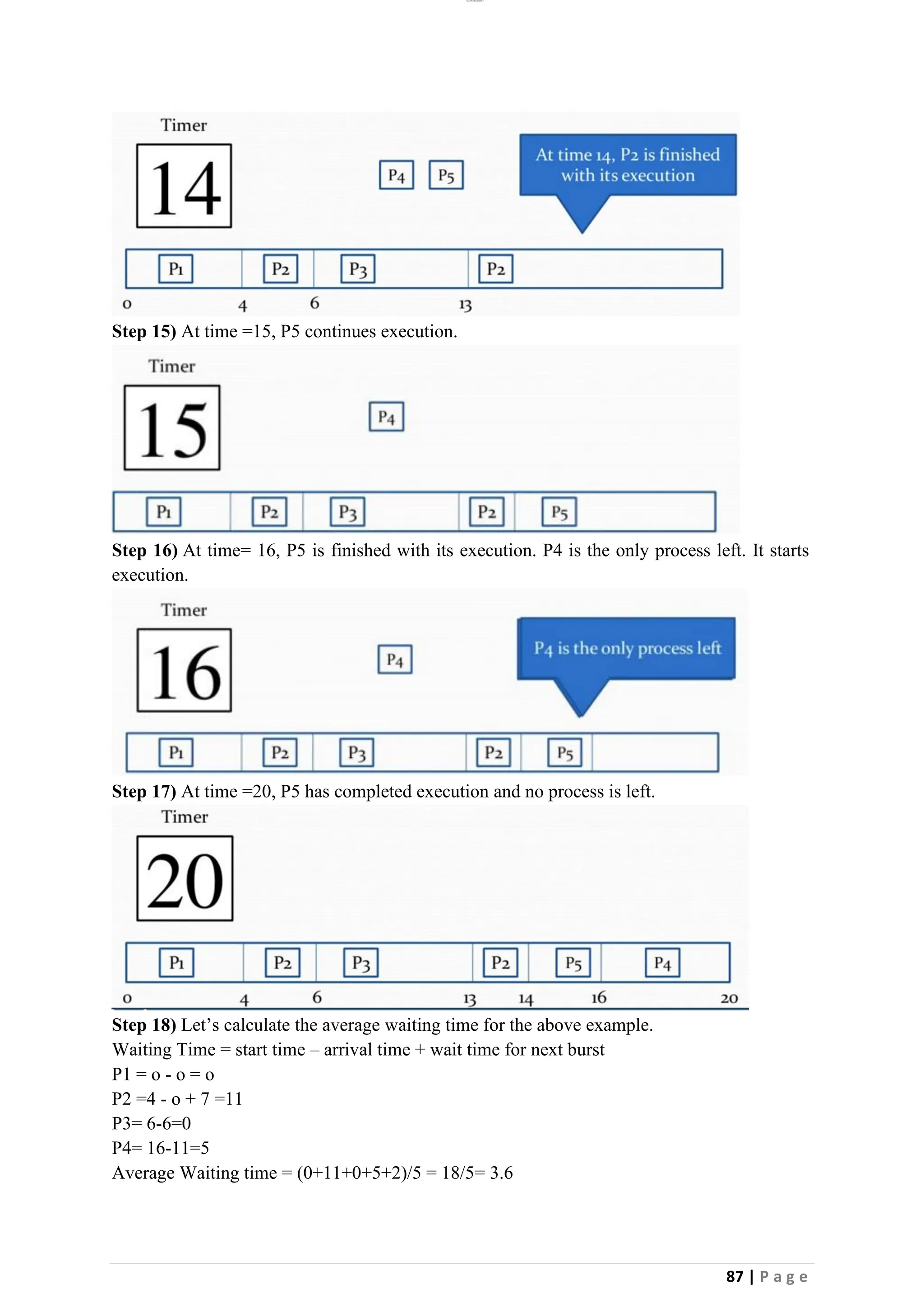
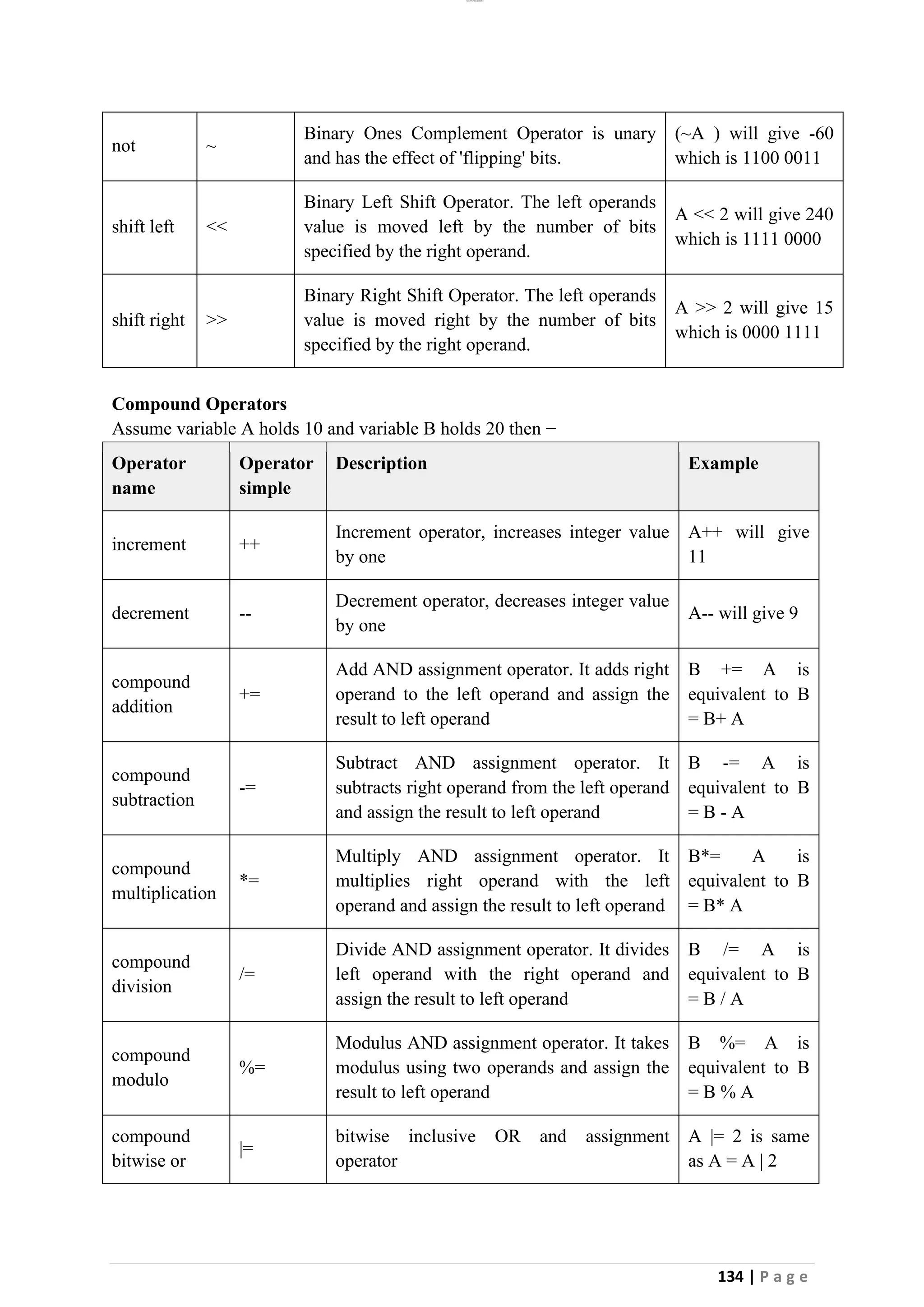
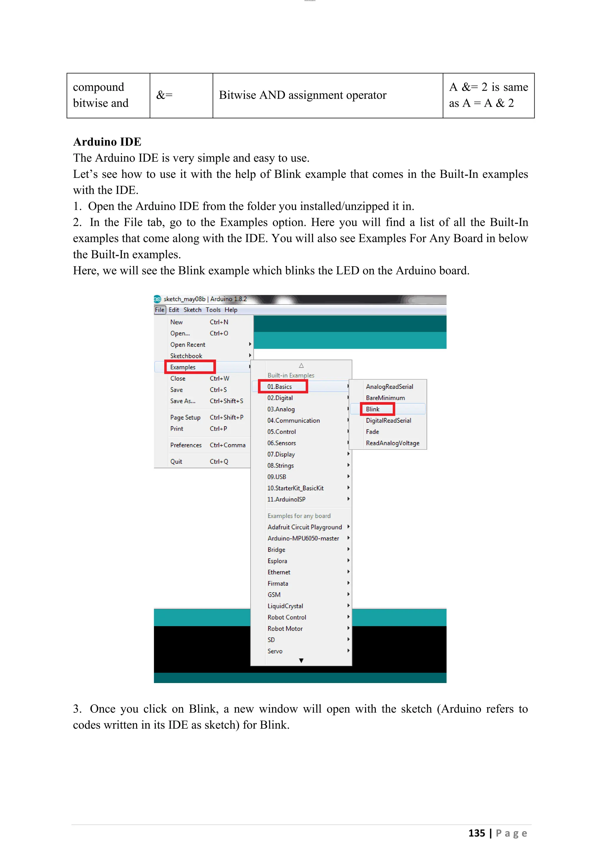
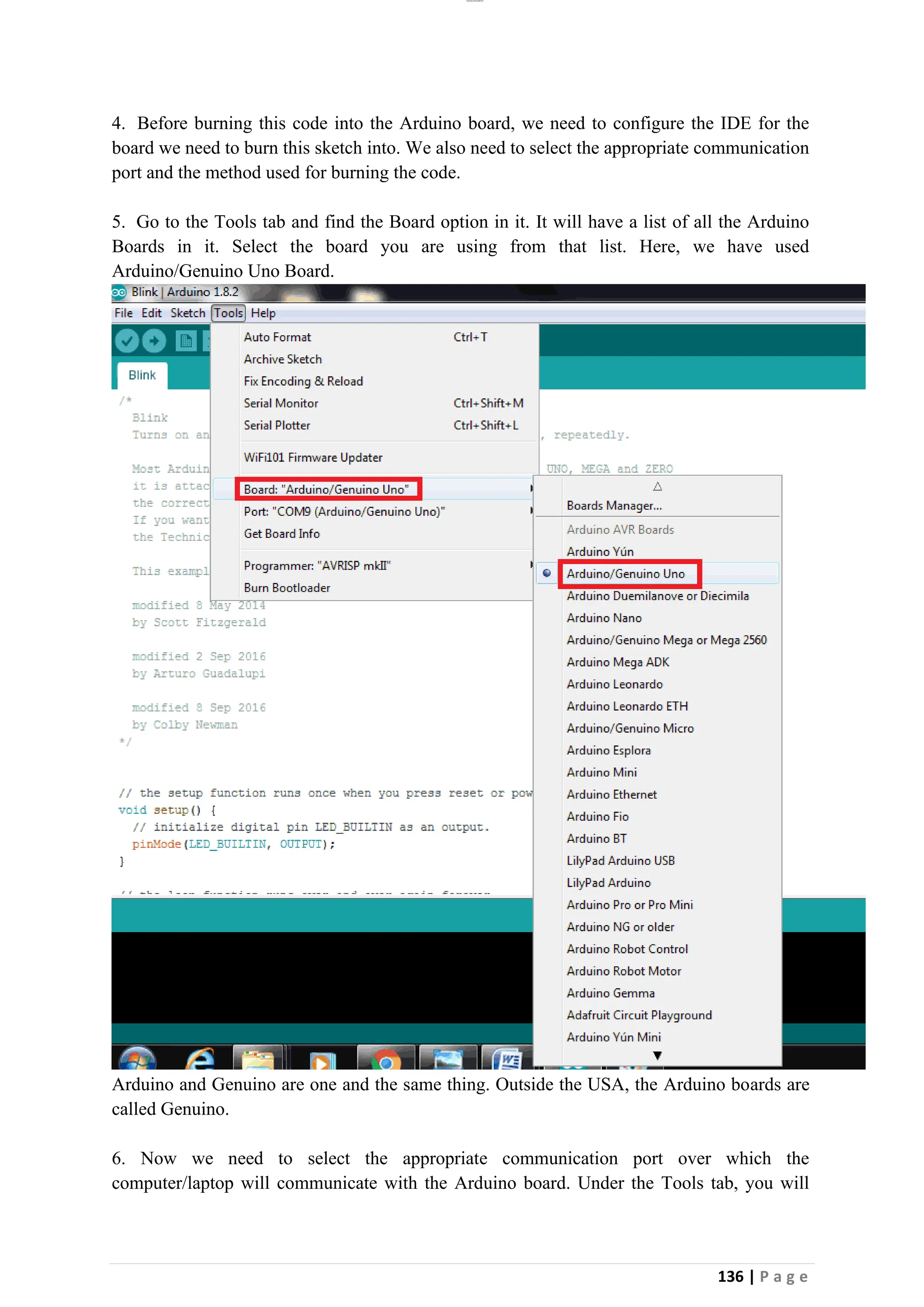
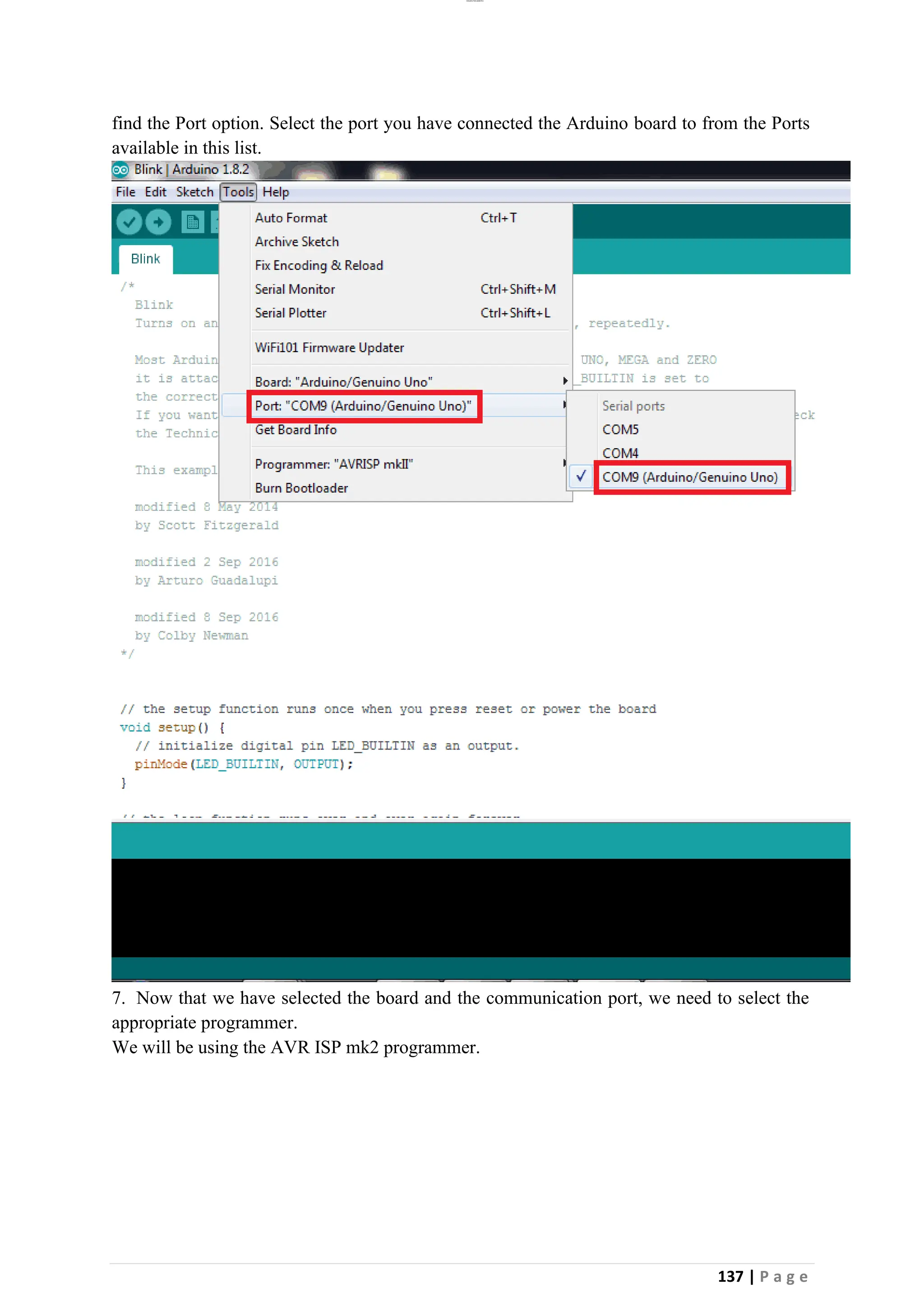
This document outlines the course objectives and units of an embedded systems and IoT course. The course aims to teach students about embedded processor architecture and programming, interfacing I/O devices, the evolution of the Internet of Things, and building low-cost embedded and IoT systems using platforms like Arduino and Raspberry Pi. The units cover topics like 8-bit embedded processors, embedded C programming, IoT and Arduino programming, IoT communication protocols, and applications development for home automation, smart agriculture, and smart cities.
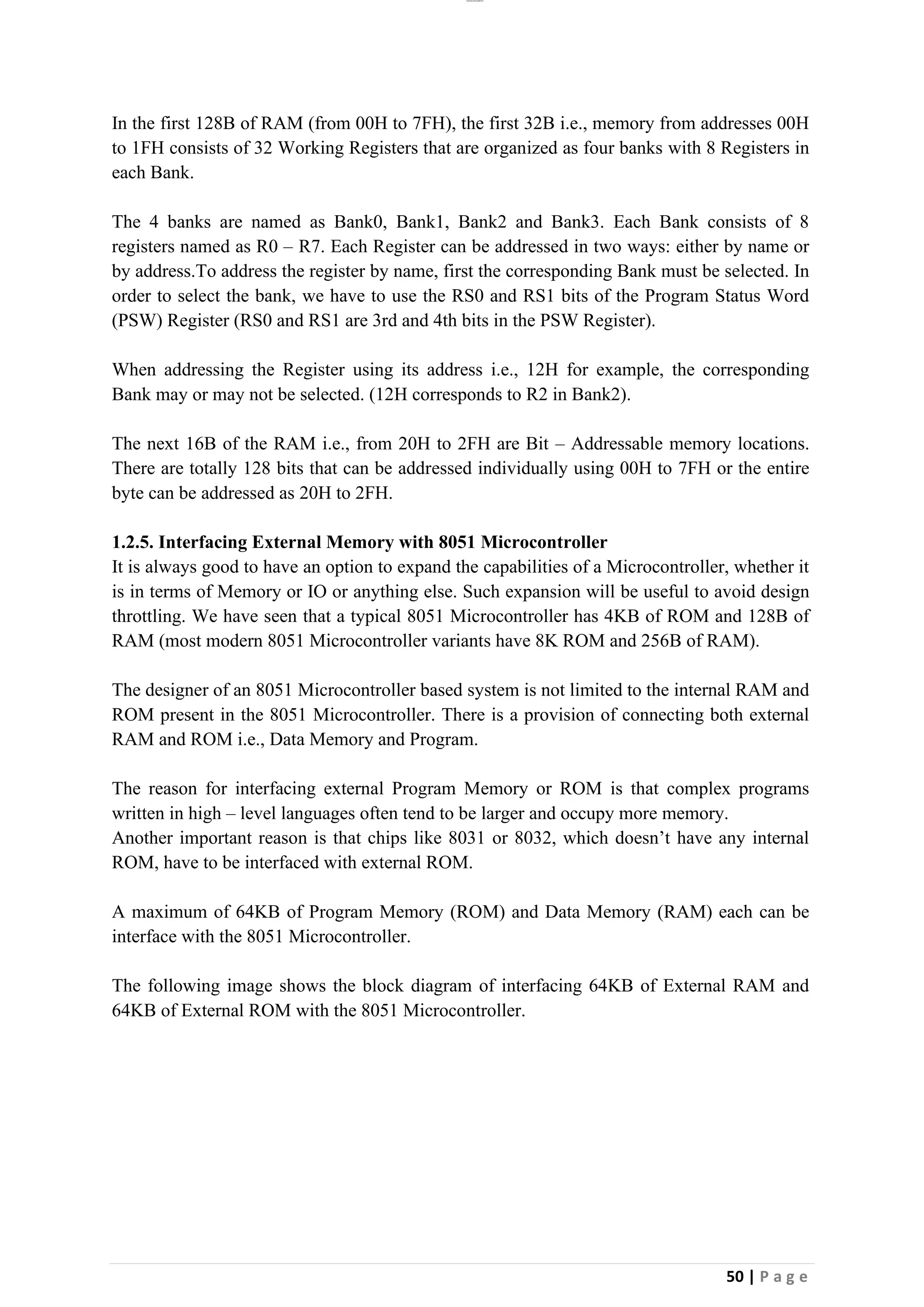
![lOMoAR cPSD|26885763
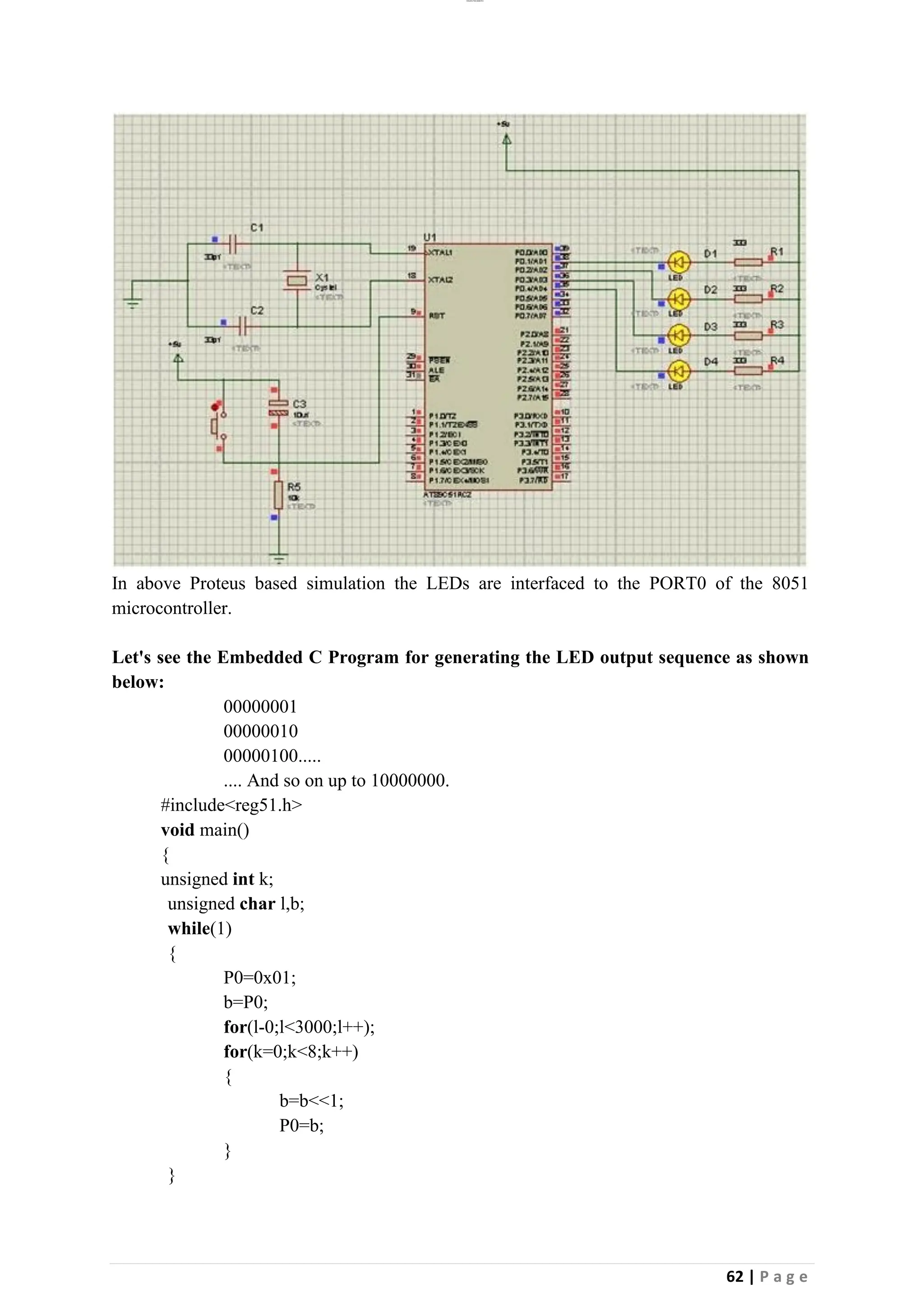
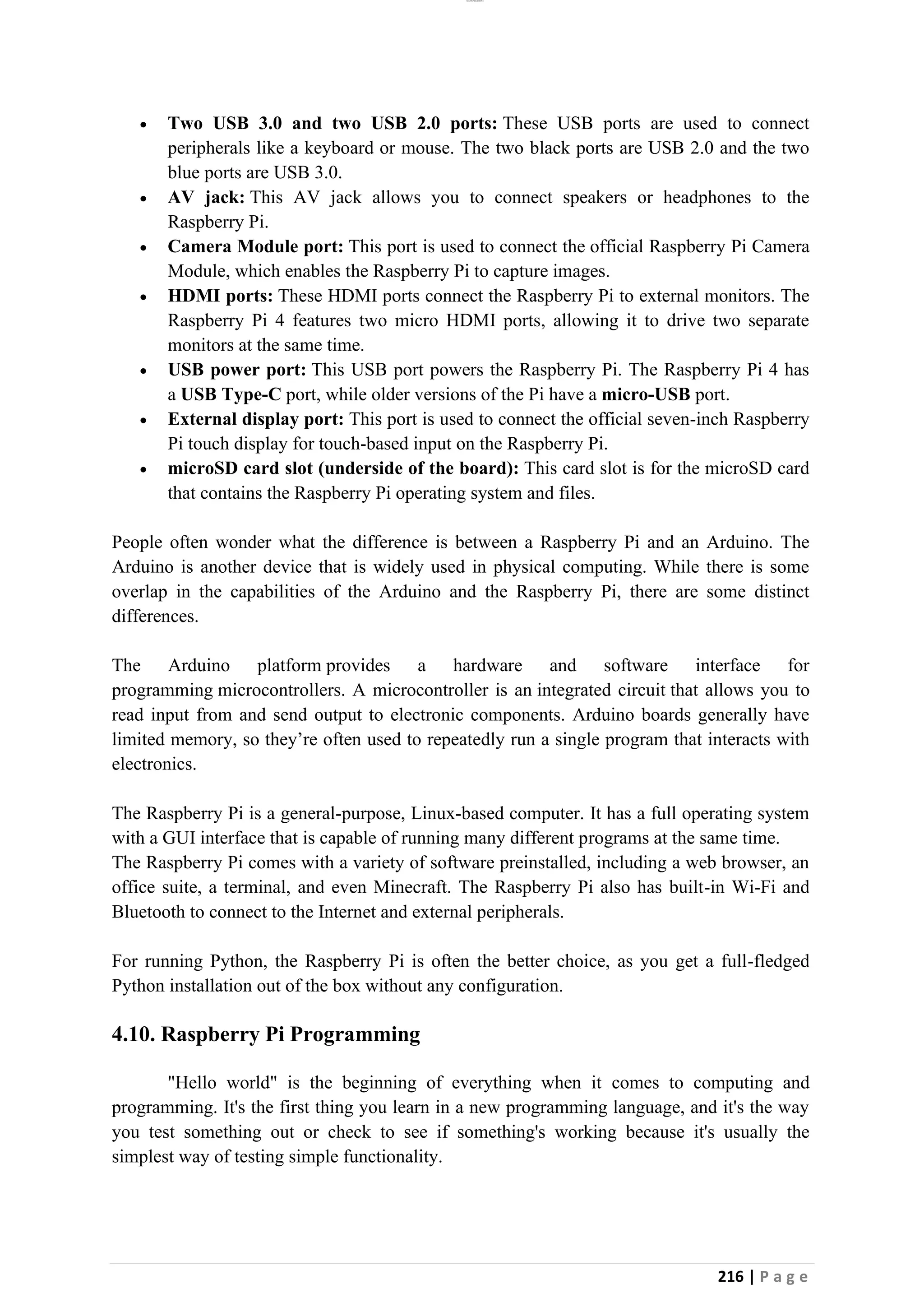
64 | P a g e
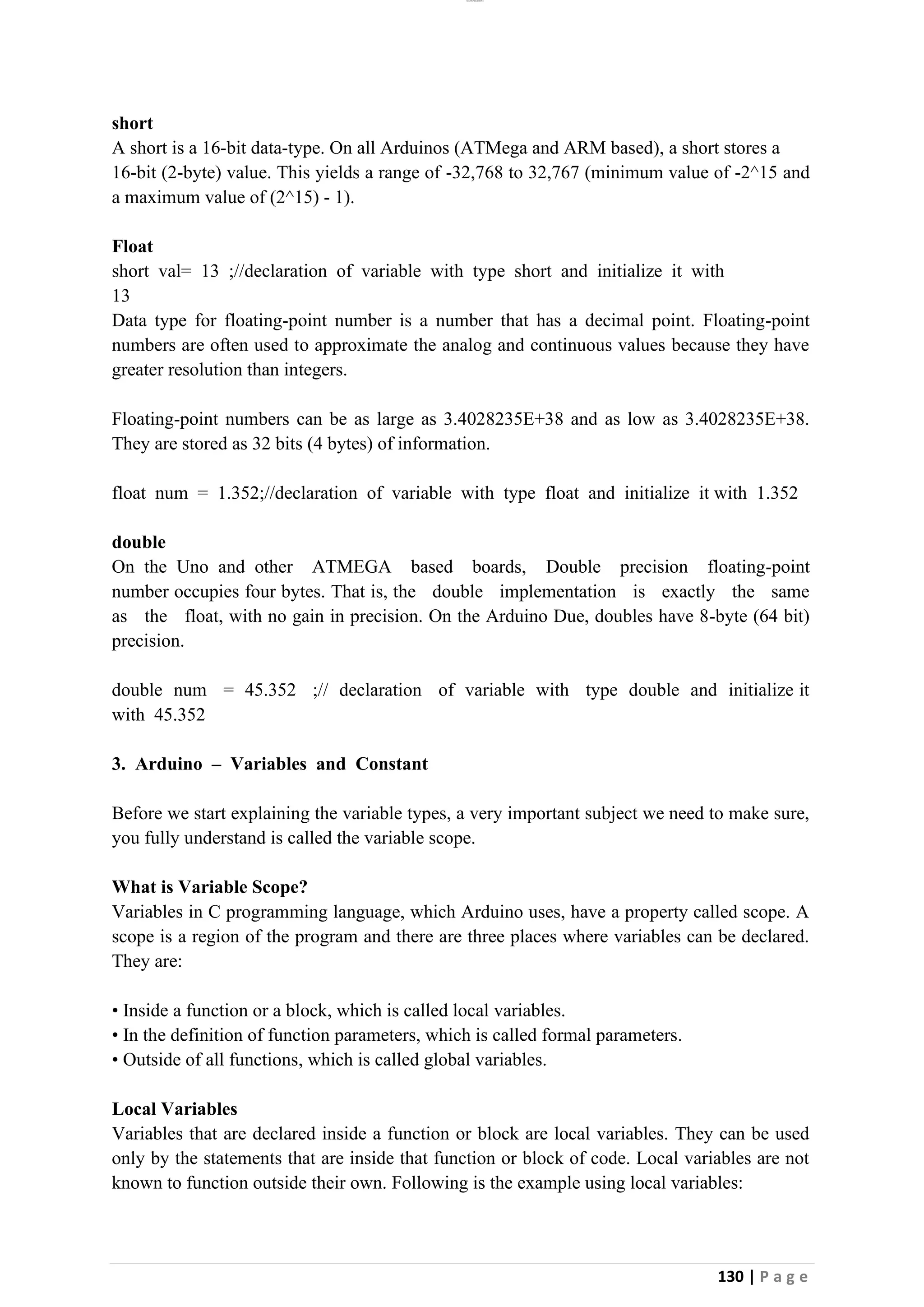
Consider the program for displaying the number from '0 to F' on 7-segment display is:-
10s
#include<reg51.h>
sbit a= P3^0;
sbit x= P3^1;
sbit y= P3^2;
sbit z= P3^3;
void main()
{
unsigned char m[10]={0?40,0xF9,0?24,0?30,0?19,0?12,0?02,0xF8,0xE00,0?10};
unsigned int i,j;
a=x=y=z=1;
while(1)
{
for(i=0;i<10;i++)
{
P2=m[i];
for(j=0;j<60000;j++);
}
}
}
Consider the program for displaying numbers from '00 to 10' on a 7segment display is:-
#include<reg51.h>
sbit x= P3^0;
sbit y= P3^1;
void display1();
void display2();
void delay();](https://image.slidesharecdn.com/cs3691embeddedsystemsandiot-240408083715-51420fb0/75/EMBEDDED-SYSTEMS-AND-IOT-lab-manual-for-enginnering-students-64-2048.jpg)
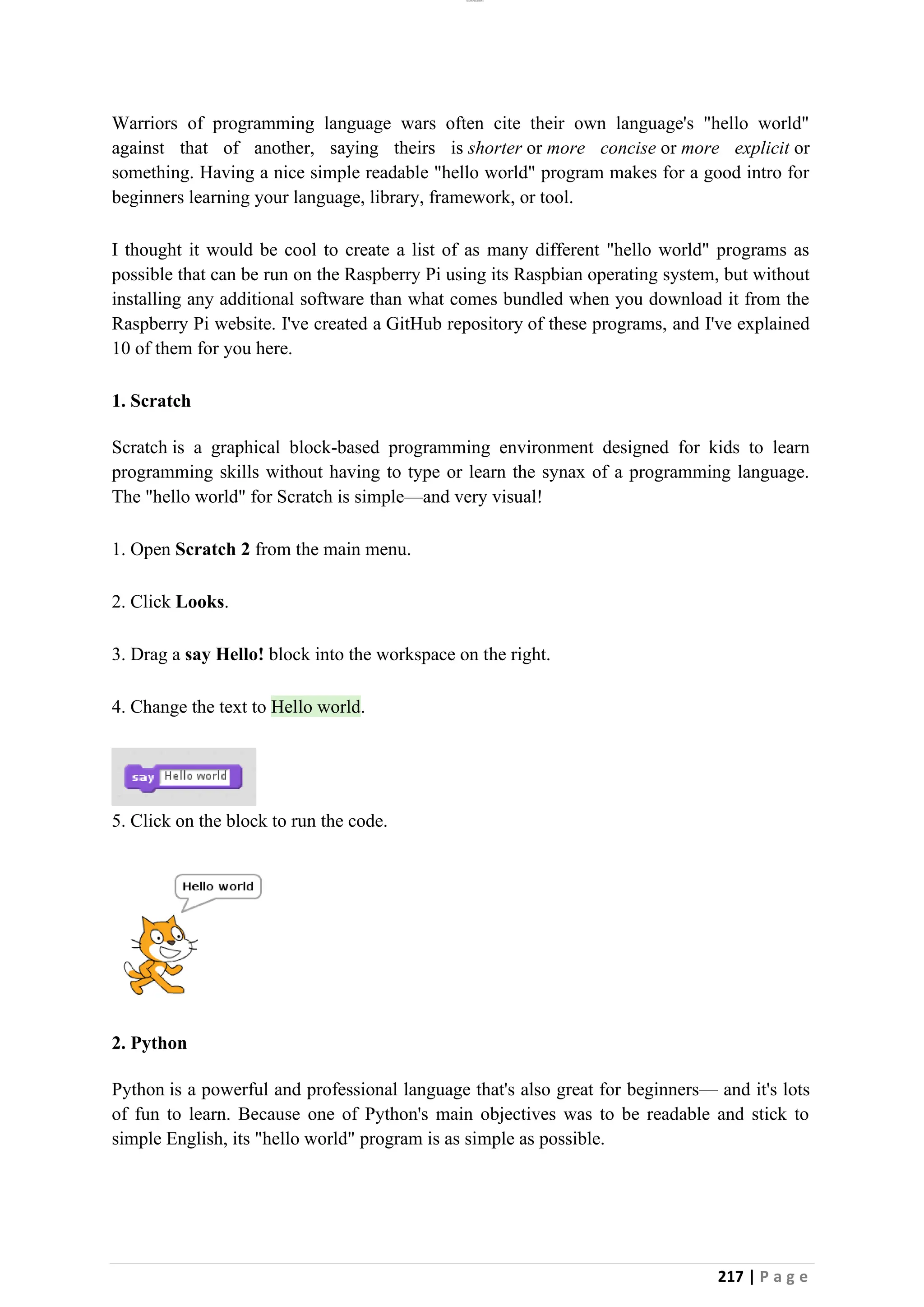
![lOMoAR cPSD|26885763
65 | P a g e
void main()
{
unsigned char m[10]={0?40,0xF9,0?24,0?30,0?19,0?12,0?02,0xF8,0xE00,0?10};
unsigned int i,j;
ds1=ds2=0;
while(1)
{
for(i=0,i<20;i++)
display1();
display2();
}
}
void display1()
{
x=1;
y=0;
P2=m[ds1];
delay();
x=1;
y=0;
P2=m[ds1];
delay();
}
void display2()
{
ds1++;
if(ds1>=10)
{
ds1=0;
ds2++;
if(ds2>=10)
{
ds1=ds2=0;
}
}
}
void delay()
{
unsigned int k;
for(k=0;k<30000;k++);
}
2.3. RTOS (Real-Time Operating Systems for Embedded Developers)](https://image.slidesharecdn.com/cs3691embeddedsystemsandiot-240408083715-51420fb0/75/EMBEDDED-SYSTEMS-AND-IOT-lab-manual-for-enginnering-students-65-2048.jpg)
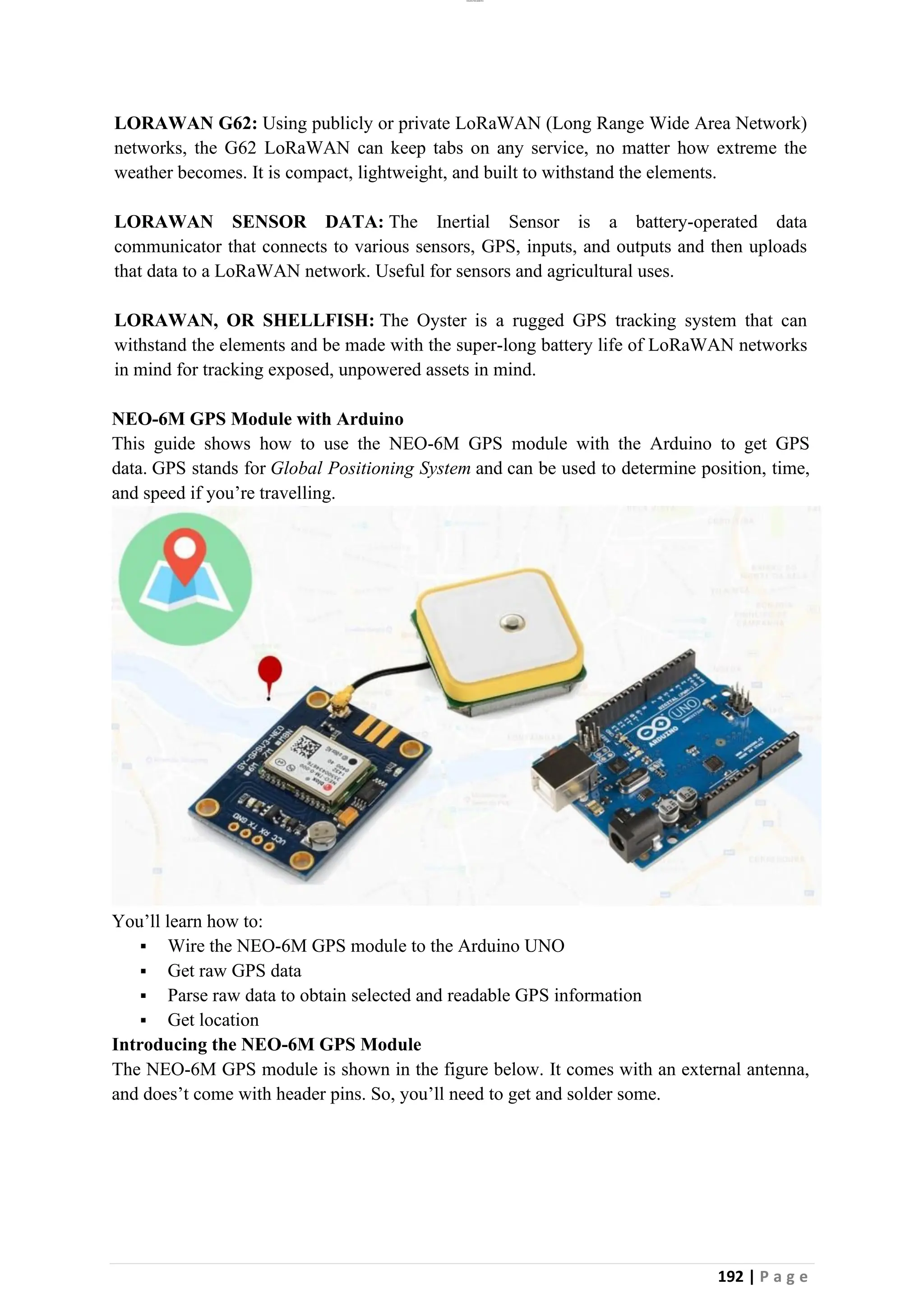
![lOMoAR cPSD|26885763
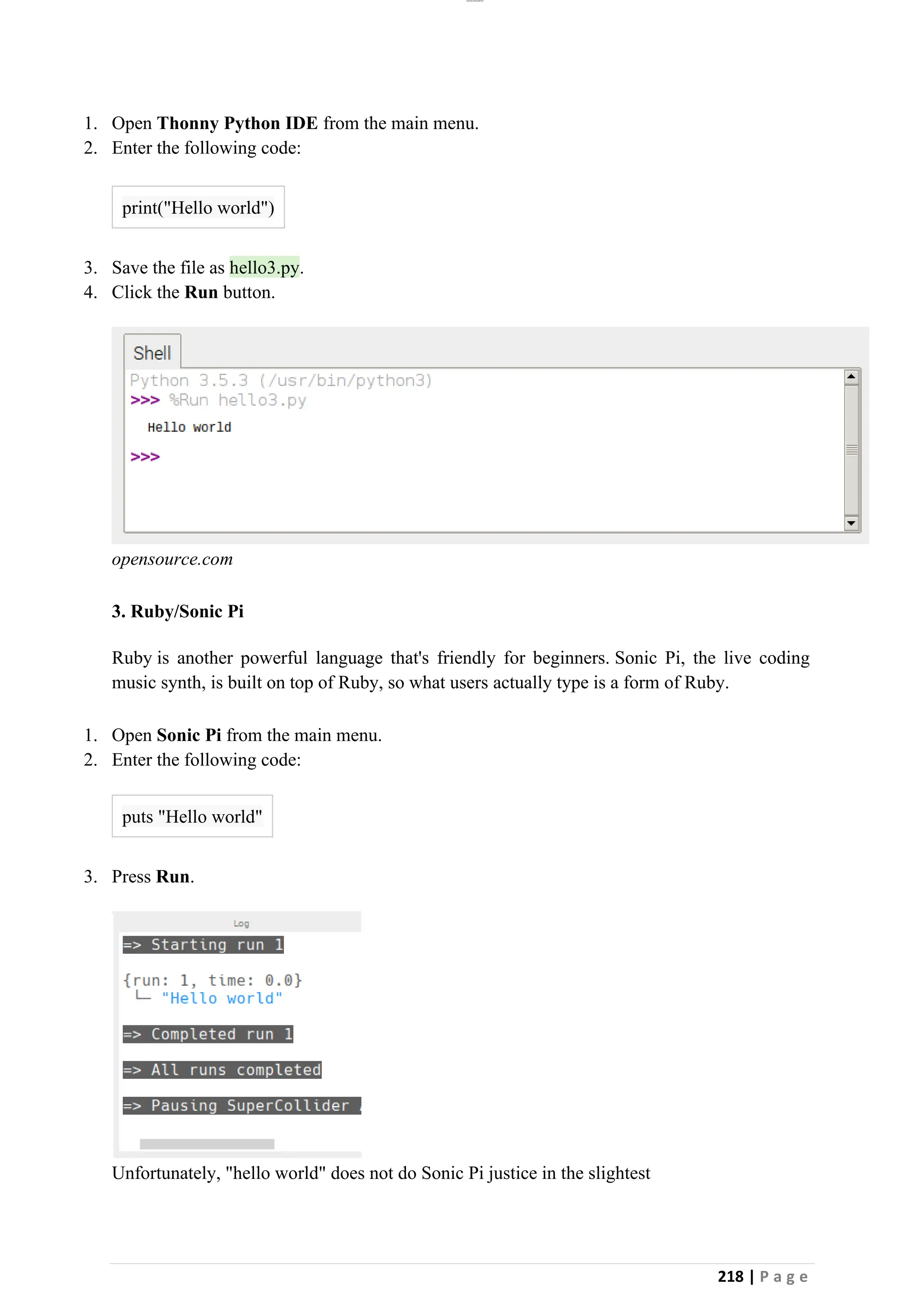
113 | P a g e
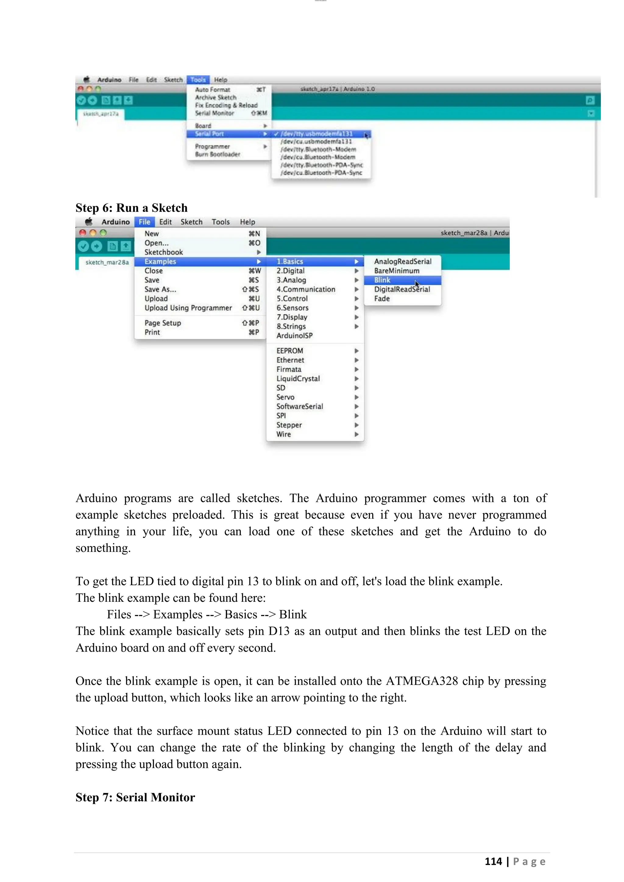
The Arduino Uno requires a male USB A to male USB B cable.
Step 5: Settings
Before you can start doing anything in the Arduino programmer, you must set the board-type
and serial port.
To set the board, go to the following:
Tools --> Boards
Select the version of board that you are using. Since I have an Arduino Uno plugged in, I
obviously selected "Arduino Uno."
To set the serial port, go to the following:
Tools --> Serial Port
Select the serial port that looks like:
/dev/tty.usbmodem [random numbers]](https://image.slidesharecdn.com/cs3691embeddedsystemsandiot-240408083715-51420fb0/75/EMBEDDED-SYSTEMS-AND-IOT-lab-manual-for-enginnering-students-113-2048.jpg)

![lOMoAR cPSD|26885763
183 | P a g e
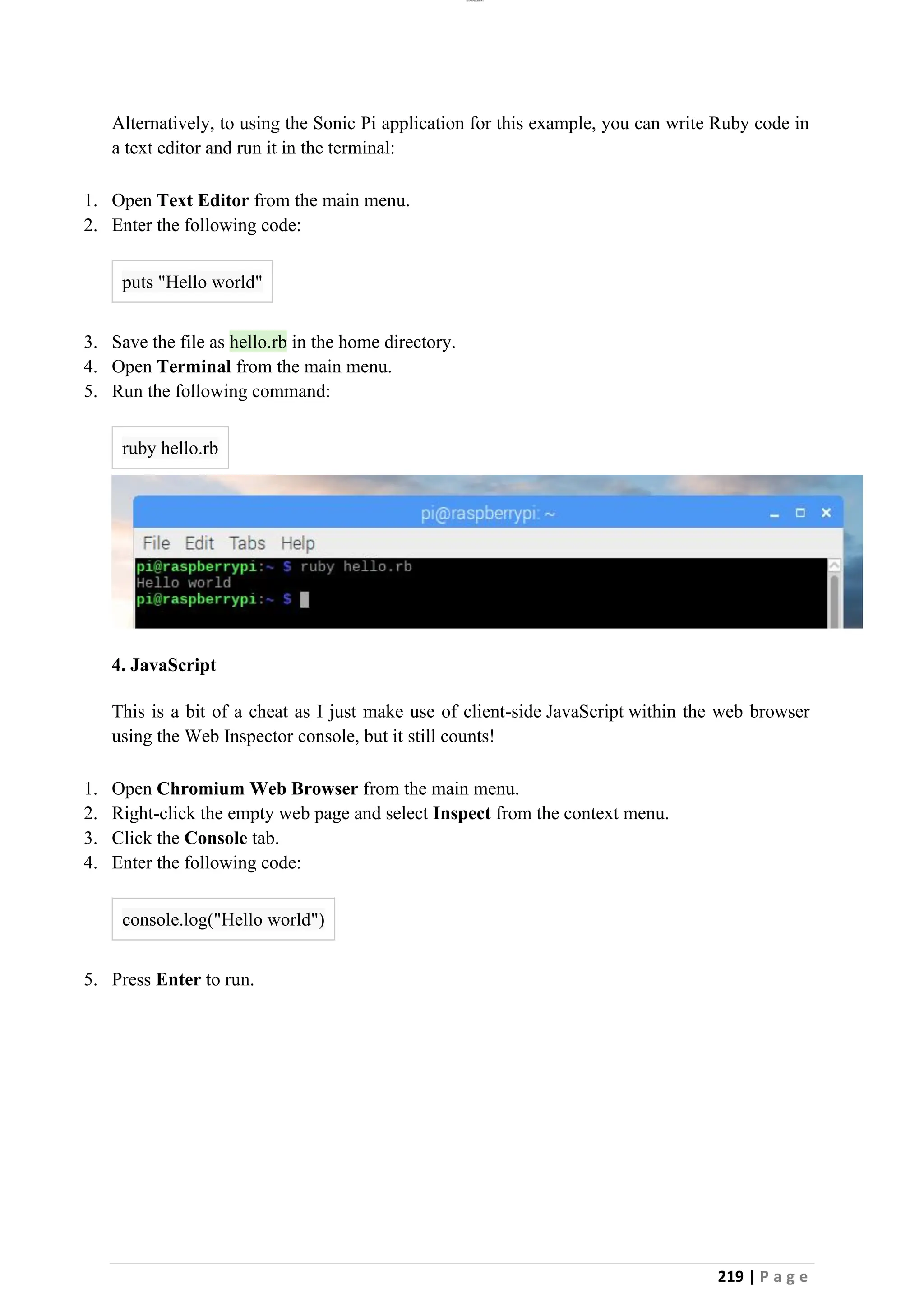
Protocol Frequency Signal Maximum data rate
Legacy 802.11 2.4 GHz FHSS or DSSS 2 Mbps
802.11a 5 GHz OFDM 54 Mbps
802.11b 2.4 GHz HR-DSSS 11 Mbps
802.11g 2.4 GHz OFDM 54 Mbps
802.11n 2.4 or 5 GHz OFDM 600 Mbps (theoretical)
802.11ac 5 GHz 256-QAM 1.3 Gbps
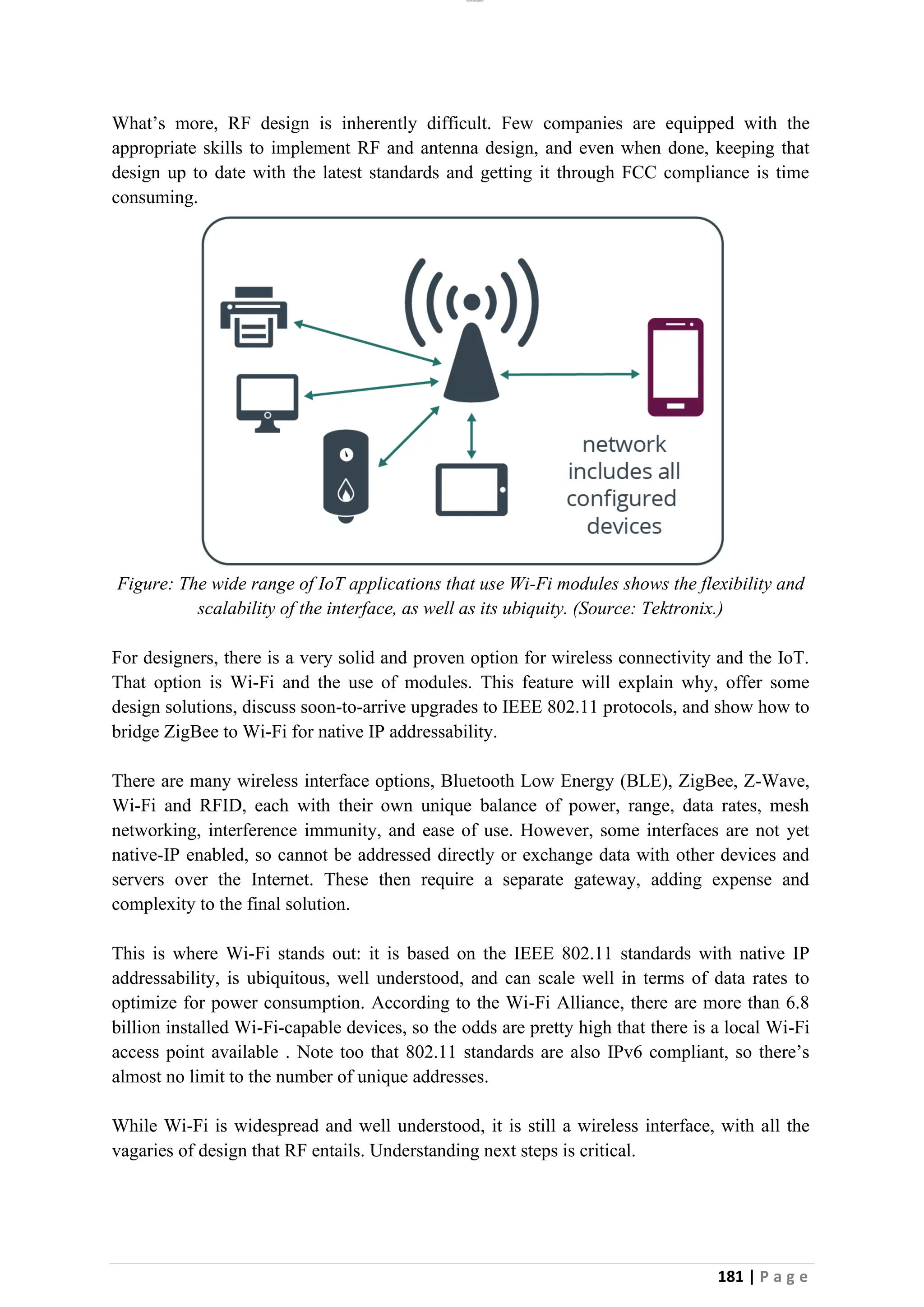
Table: A summary of different Wi-Fi protocols and data rates shows the progression of IEEE
802.11 from its early days of 2 Mbps to 1.3 Gbps today. (Source: Intel Corp.)
When designing for IoT applications, however, a higher data rate protocol is not always
preferable. Even though 802.11ac can crank it up to a maximum of 1.3 Gbps, most embedded
applications (e.g., machine to machine [M2M] data and control devices) are power
constrained and can get by with a much lower data rate.
One more good reason to choose Wi-Fi is that within the next year or so technology upgrades
will make it much more capable. For example, the Wi-Fi Alliance recently announced the
Wi-Fi HaLow (pronounced "halo") designation for products incorporating IEEE 802.11ah
technology. HaLow extends Wi-Fi into the 900 MHz band and offers improved range –
nearly twice that of today’s Wi-Fi – with scalable data rates from 150 Kbps to 2.1 Mbps;
IEEE 802.11ah also promises to provide low power consumption features and its use cases
are primarily for wireless sensor networks, a classic IoT application.
In February, at the 2016 International Solid-State Circuits Conference (ISSCC) the Holst
Centre of the Netherlands, in collaboration with Belgium’s IMEC Research Institute, showed
a HaLow transmitter running Wi-Fi over sub-GHz bands. The team cited a maximum power
consumption of 7.1 mW when delivering 0 dBm output power and operating from a 1 V
supply. This represents a 10x power reduction compared to state-of-the-art 802.11 OFDM
transceivers.
Also under development is IEEE 802.11ai, which will provide a fast initial link setup
(achieving a secure link setup in less than 100 ms) and IEEE 802.11aq, being developed to
provide a cellular-like automatic network-discovery experience.
Modules and dev kits
RF engineering can be a tricky business, especially for neophytes in the discipline.
Recognizing this, RF silicon suppliers are providing modules, dev kits and reference designs
that make adding wireless connectivity to a product much easier.](https://image.slidesharecdn.com/cs3691embeddedsystemsandiot-240408083715-51420fb0/75/EMBEDDED-SYSTEMS-AND-IOT-lab-manual-for-enginnering-students-183-2048.jpg)

![lOMoAR cPSD|26885763
221 | P a g e
Java is a popular language in industry, and is commonly taught to undergraduates studying
computer science. I learned it at university and have tried to avoid touching it since then.
Apparently, now I do (very small amounts of) it for fun...
1. Open Text Editor from the main menu.
2. Enter the following code:
3. publicclassHello {
4. publicstaticvoidmain(String[] args) {
5. System.out.println("Hello world");
6. }
7. }
8.
9. Save the file as Hello.java in the home directory.
10. Open Terminal from the main menu.
11. Run the following commands:
12. javac Hello.java
java Hello
I could almost remember the "hello world" for Java off the top of my head, but not quite. I
always forget where the String[] args bit goes, but it's obvious when you think about it...
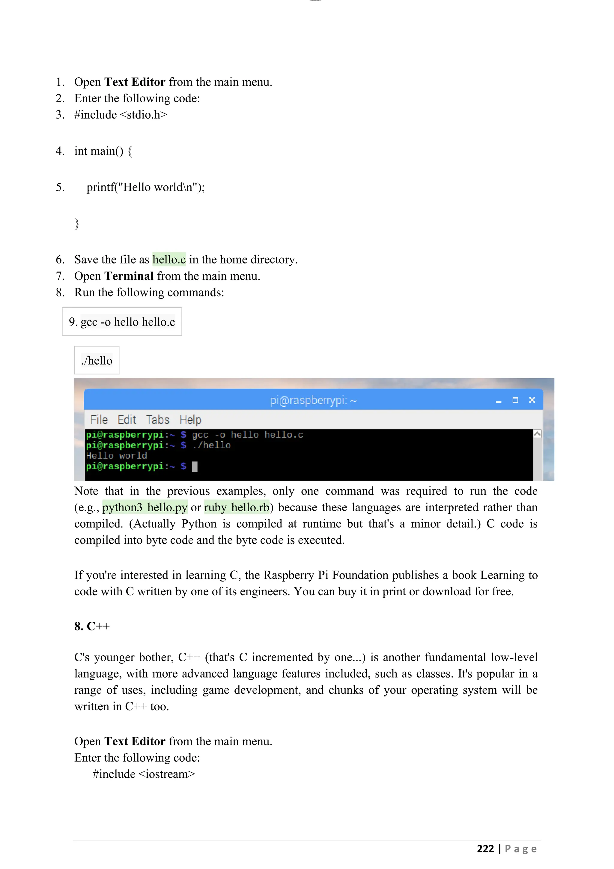
7. C
C is a fundamental low-level programming language. It's what many programming languages
are written in. It's what operating systems are written in. See for yourself&mdash:take a look
at the source for Python and the Linux kernel. If that looks a bit hazy, get started with "hello
world":](https://image.slidesharecdn.com/cs3691embeddedsystemsandiot-240408083715-51420fb0/75/EMBEDDED-SYSTEMS-AND-IOT-lab-manual-for-enginnering-students-221-2048.jpg)