The document provides an introduction to analog and digital electronics. It discusses:
1) The prerequisites for the course including basic electrical engineering, C programming, and basic electronics.
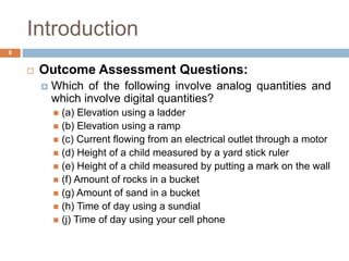
2) The differences between analog and digital representations, with analog being continuous and digital being discrete.
3) Some key aspects of digital electronics including binary numbers, parallel vs serial transmission, memory, and the major parts of a digital computer like input, output, memory, arithmetic/logic, and control units.
4) An overview of semiconductor devices like photodiodes, light emitting diodes (LEDs), and photocouplers along with their basic construction, working principles, and applications.
5) Different biasing
4. Introduction
Outcome Assessment Questions
What are the two numeric digits used to represent
states in a digital system?
What are the two terms used to represent the two
logic levels?
What is the abbreviation for binary digit?
4
5. Introduction
Digital Signals
The transition between the two states is called an
edge.
At dawn, when the signal proceeds from HIGH to
LOW, it is considered a falling edge, or negative
edge.
5
6. Introduction
Need for Timing Digital
To show the relationship between changes at the
input and changes at the output in order to
demonstrate the operation of the system.
This means the logic states must be observed
over time.
Timing diagrams show the relationship, over time,
between many digital “signals.”
6
7. Introduction
Analog and Digital Representations
Analog representation a quantity is represented by a
continuously variable, proportional indicator.
E.g.
Speedometer
Thermometers
Digital representation the quantities are represented not
by continuously variable indicators but by symbols called
digits.
E.g.
Digital Speedometer
Digital indoor/outdoor thermometer
The major difference between analog and digital quantities,
then, can be simply stated as follows:
Analog ≡ continuous
Digital ≡ discrete (step by step)
7
8. Introduction
Outcome Assessment Questions:
Which of the following involve analog quantities and
which involve digital quantities?
(a) Elevation using a ladder
(b) Elevation using a ramp
(c) Current flowing from an electrical outlet through a motor
(d) Height of a child measured by a yard stick ruler
(e) Height of a child measured by putting a mark on the wall
(f) Amount of rocks in a bucket
(g) Amount of sand in a bucket
(h) Time of day using a sundial
(j) Time of day using your cell phone
8
9. Introduction
Digital and Analog systems
A digital system is a combination of devices designed to
manipulate logical information or physical quantities that
are represented in digital form; that is, the quantities can
take on only discrete values.
These devices are most often electronic, but they can
also be mechanical, magnetic, or pneumatic.
An analog system contains devices that manipulate
physical quantities that are represented in analog form.
In an analog system, the quantities can vary over a
continuous range of values.
For example, the amplitude of the output signal to the
speaker in a radio receiver can have any value between
zero and its maximum limit.
9
10. Introduction
Advantages of Digital Techniques
Digital systems are generally easier to design
Information storage is easy
Accuracy and precision are easier to maintain throughout the
system
Operations can be programmed
Digital circuits are less affected by noise
More digital circuitry can be fabricated on IC chips
10
11. Introduction
Limitations of Digital Techniques
The real world is analog and digitizing always introduces
some error. Processing digitized signals takes time.
To take advantage of digital techniques when dealing with analog
inputs and outputs, four steps must be followed:
1. Convert the physical variable to an electrical signal (analog).
2. Convert the electrical (analog) signal into digital form.
3. Process (operate on) the digital information.
4. Convert the digital outputs back to real-world analog form.
11
13. Introduction
13
Digital Number Systems
Decimal System
The decimal system is composed of 10 numerals or
symbols. These 10 symbols are 0, 1, 2, 3, 4, 5, 6, 7, 8,
9. The decimal system, also called the base-10.
Decimal position values as powers of 10.
15. Introduction
15
Binary System
Unfortunately, the decimal number system does not
lend itself to convenient implementation in digital
systems.
For example, it is very difficult to design electronic
equipment so that it can work with 10 different voltage
levels (each one representing one decimal character, 0
through 9).
On the other hand, it is very easy to design simple,
accurate electronic circuits that operate with only two
voltage levels.
For this reason, almost every digital system uses the
binary (base-2) number system as the basic number
system of its operations
19. Introduction
19
Parallel and Serial Transmission
Parallel transmission uses one connecting line
per bit, and all bits are transmitted
simultaneously;
Serial transmission uses only one signal line,
and the individual bits are transmitted serially
(one at a time).
21. Introduction
21
Memory
When an input signal is applied to most devices or
circuits, the output somehow changes in response to
the input, and when the input signal is removed, the
output returns to its original state. These circuits do
not exhibit the property of memory because their
outputs revert back to normal.
Certain types of devices and circuits do have memory.
When an input is applied to such a circuit, the output
will change its state, but it will remain in the new state
even after the input is removed. This property of
retaining its response to a momentary input is called
memory.
25. Referred Books/Sources
Charles H Roth and Larry L Kinney, Analog
and Digital Electronics, Cengage Learning,
2019
Robert L. Boylestad Louis Nashelsky :
Electronic Devices and Circuit Theory,
Eleventh Edition, 2013.
Albert Malvino, David J. Bates : Electronic
principles, Eighth edition, 2016.
Thomas L. Floyd: Electronic Devices, Ninth
Edition, Prentice Hall, 2012
25
26. Objectives
OP-Amp
Peak Detector Circuit, Active Filters, Non-Linear
Amplifier, Relaxation Oscillator Current-To-
Voltage Converter, Voltage-To-Current Converter.
Multivibrator circuits configuration around
digital integrated circuits,
Multivibrator circuits configured around timer IC
555.
26
29. Photodiode
29
The photodiode is a semiconductor p – n
junction device whose region of operation is
limited to the reverse-bias region.
The reverse saturation current is normally limited
to a few microamperes.
It is due solely to the thermally generated minority
carriers in the n - and p -type materials.
The application of light to the junction will result in
a transfer of energy from the incident traveling
light waves (in the form of photons) to the atomic
structure, resulting in an increased number of
minority carriers and an increased level of reverse
current.
31. Photodiode
31
Construction
The surface of a layer of N type is bombarded with P type silicon
ions to produce a P type layer about 1 µm (micrometre) thick.
During the formation of the diode, electrons from the N type layer
are attracted into the P type material and holes from the P type are
attracted into the N type layer, resulting in the removal of free
charge carriers close to the PN junction, so creating a depletion
layer.
The (light facing) top of the diode is protected by a layer of Silicon
Dioxide (SiO2) in which there is a window for light to shine on the
semiconductor.
This window allow maximum absorption of light and an anode
connection of aluminium (Al) is provided to the P type layer.
Beneath the N type layer is a more heavily doped N+ layer to
provide a low resistance connection to the cathode.
33. Photodiode
33
Working Principle
Recall that when reverse-biased, a rectifier diode has a very small
reverse leakage current.
The same is true for a photodiode.
The reverse-biased current is produced by thermally generated
electron-hole pairs in the depletion region, which are swept across
the pn-junction by the electric field created by the reverse voltage.
In a rectifier diode, the reverse leakage current increases with
temperature due to an increase in the number of electron-hole
pairs.
A photodiode differs from a rectifier diode in that when its pn
junction is exposed to light, the reverse current increases with the
light intensity.
When there is no incident light, the reverse current, is almost
negligible and is called the dark current.
An increase in the amount of light intensity, expressed as irradiance
(mW/cm2), produces an increase in the reverse current,
35. Light Emitting Diode (LED)
35
The increasing use of digital displays in
calculators, watches, and all forms of
instrumentation has contributed to an extensive
interest in structures that emit light when properly
biased.
The light-emitting diode is a diode that gives off
visible or invisible (infrared) light when energized.
The energy converted during recombination at the
junction is dissipated in the form of heat within the
structure, and the emitted light.
Diodes constructed of GaAs emit light in the
infrared (invisible) zone during the recombination
process at the p–n junction.
36. Light Emitting Diode (LED)
36
The below table provides a list of common
compound semiconductors and the light they
generate.
37. Light Emitting Diode (LED)
37
Construction
Process of electroluminescence in the LED, graphic symbol and Parts of an
LED
38. Light Emitting Diode (LED)
38
Construction
The external metallic conducting surface
connected to the p -type material is smaller to
permit the emergence of the maximum number
of photons of light energy when the device is
forward-biased. Note in the figure that the
recombination of the injected carriers due to
the forward-biased junction results in emitted
light at the site of the recombination.
39. Light Emitting Diode (LED)
39
Working Principle
When the device is forward-biased, electrons cross the pn junction from the n-type material and
recombine with holes in the p-type material.
These free electrons are in the conduction band and at a higher energy than the holes in the
valence band.
The difference in energy between the electrons and the holes corresponds to the energy of visible
light.
When recombination takes place, the recombining electrons release energy in the form of
photons.
The emitted light tends to be monochromatic (one color) that depends on the band gap (and other
factors).
A large exposed surface area on one layer of the semiconductive material permits the photons to
be emitted as visible light.
This process, called electroluminescence,
40. Light Emitting Diode (LED)
40
Working Principle
• The forward voltage across an LED is considerably greater than for a silicon
diode.
• Typically, the maximum VD for LEDs is between 1.2 V and 3.2 V, depending
on the material.
• Reverse breakdown for an LED is much less than for a silicon rectifier diode
(3 V to 10 V is typical).
• The LED emits light in response to a sufficient forward current.
• The amount of power output translated into light is directly proportional to the
forward current.
• An increase in ID corresponds proportionally to an increase in light output.
• The light output (both intensity and color) is also dependent on temperature.
41. Light Emitting Diode (LED)
41
Applications
TV Remote, Calculator, Traffic Signals,
Watches and Automotive Head Lamps
42. Photocoupler (Optocoupler)
42
Construction
An optocoupler (also called an optoisolator) combines
an LED and a photodiode in a single package.
Figure shows an optocoupler.
It has an LED on the input side and a photodiode on
the output side.
The left source voltage and the series resistor set up a
current through the LED.
43. Photocoupler (Optocoupler)
43
Working Principle
Then the light from the LED hits the photodiode,
and this sets up a reverse current in the output
circuit.
This reverse current produces a voltage across
the output resistor.
The output voltage then equals the output supply
voltage minus the voltage across the resistor.
When the input voltage is varying, the amount of
light is fluctuating. This means that the output
voltage is varying in step with the input voltage.
This is why the combination of an LED and a
photodiode is called an optocoupler.
46. Introduction
46
The term biasing is an all-inclusive term for
the application of dc voltages to establish a
fixed level of current and voltage.
For transistor amplifiers the resulting dc
current and voltage establish an operating
point on the characteristics that define the
region that will be employed for amplification
of the applied signal.
Because the operating point is a fixed point on
the characteristics, it is also called the
quiescent point (abbreviated Q -point).
47. Introduction
47
Following important basic relationships for a
transistor:
VBE = 0.7 V
IE = (β + 1)IB ≈ IC
IC = βIB
Types of Biasing
Base Bias or Fixed Bias
Collector to Base Bias
Voltage Divider Bias
48. Base Bias or Fixed Bias
Circuit Diagram Apply KVL at input
side or Base Emitter
Side So,
+VCC – IBRB – VBE =
0
The current IB is :
Now IC = βIB
48
49. Base Bias or Fixed Bias
Circuit Diagram Apply KVL at output side or
Collector Emitter Side So,
VCE + ICRC – VCC = 0
and
VCE = VCC – ICRC
From Circuit
VCE = VC – VE
VBE = VB – VE
and VE = 0V
So
VCE = VC
VBE = VB
49
50. Collector to Base Bias
Circuit Diagram The current through
RC is not IC , but
I’C. where I’C = IC +
IB.
However, the level of
IC and I’C far
exceeds the usual
level of IB, and the
approximation IC≈I’C is
normally employed.
Substituting IC ≈ IC =
βIB and IE ≈ IC
50
51. Collector to Base Bias
Circuit Diagram From input side of the circuit
VCC – I’CRC – IBRF – VBE – IERE
= 0
So
VCC– βIBRC – IBRF – VBE –
βIBRE = 0
VCC – IBRF – VBE – βIB(RE +
RC)= 0
Now
51
52. Collector to Base Bias
Circuit Diagram Apply KVL at output side or
Collector Emitter Side So,
IERE + VCE + I’CRC – VCC =
0
I’C ≈ IC and IE ≈ IC
We have
IC(RC + RE) + VCE – VCC = 0
and
VCE = VCC – IC(RC + RE)
52
53. Voltage Divider Bias
Circuit Diagram Let I1 and I2 are
current through R1
and R2.
From circuit (apply
KCL)
I1 = IB + I2
The current IB is much
smaller than I2.
So I1 = I2
The voltage across
R2, which is actually
the base voltage can
be determined using
the voltage-divider
53
54. Voltage Divider Bias
Circuit Diagram VB is determined,
the level of VE can
be calculated from
VBE = VB – VE
VE = VB – VBE
and the emitter
current can be
determined from
and ICQ ≈ IE
54
55. Voltage Divider Bias
Circuit Diagram The collector-to-emitter
voltage is determined by
VCE = VCC – ICRC – IERE
but because IE ≈ IC,
VCEQ = VCC – IC(RC + RE)
55
57. Introduction to Operational
Amplifier
Ideal v/s practical Op-amp
57
Difference between Ideal and Practical Op-
Amp
Parameters Ideal Op-Amp
Practical Op-Amp
(E.g. LM 741)
Bandwidth (BW) Infinite 1MHz
Slew Rate (SR) Infinite 0.5 V / μs
Open loop gain (AOL) Infinite 200,000
Common Mode
Rejection Ratio (CMRR)
Infinite 90 dB
Power Supply Rejection
Ratio (PSRR)
Zero
120 dB (+Supply)
110 dB (-Supply)
Input impedance (Ri) Infinite 2 MΩ
Output impedance (Ro) Zero 75 Ω
Offset and Offset Drifts Zero 1mV, 20nA
61. Peak Detector Circuit
61
During +ve half cycle when the input voltage is positive, the diode is
conducting/ON and capacitor charges to the peak of the input
voltage.
Second, when the input voltage is negative during –ve half cycle,
the diode is non-conducting/OFF and the capacitor discharges
through the load resistor.
As long as the discharging time constant is much greater than the
period of the input signal (T), the output voltage will be
approximately equal to the peak value of the input voltage.
This can achieved by making discharging time constant RC can be
made much longer than the period of the input signal (RC ≥ 10 T),
will get almost perfect peak detection of low-level signals.
If the peak-detected signal has to drive a small load, to avoid
loading effects by connecting the voltage follower (op-amp buffer)
isolates the small load resistor from the peak detector. This
prevents the small load resistor from discharging the capacitor too
quickly.
62. Comparator
62
Comparator circuit compares a single voltage
on one input of op-amp with a known voltage
called reference voltage (Trip point or trigger
point) on the other input and produces high or
low output depending upon relative magnitude
of two input.
Comparators with Zero Reference
Comparators with Nonzero References
Comparators with Hysteresis or Schmitt Trigger
Window Comparator
63. Comparator
Comparators with Zero Reference
63
Non-Inverting Comparator
Because of the high open-loop voltage gain, a positive input voltage
produces positive saturation, and a negative input voltage produces
negative saturation.
Above circuit is called a zero-crossing detector because the
output voltage ideally switches from low to high or vice versa
whenever the input voltage crosses zero (input compares with zero
reference voltage).
65. Comparator
Comparators with Zero Reference
65
Inverting Comparator
The input signal drives the inverting input of the comparator.
In this case, a positive input voltage produces a maximum
negative saturation, as shown in above diagram. On the other
hand, a negative input voltage produces a maximum positive
saturation.
67. Comparator
Comparators with Nonzero
References
67
Non-Inverting Comparator: Positive reference
When Vin is greater than Vref, the differential input voltage is
positive and the output voltage is high (+Vsat). When Vin is less
than Vref, the differential input voltage is negative and the output
voltage is low (-Vsat).
Vin > Vref then Vout = +Vsat
Vin < Vref then Vout = - Vsat
71. Comparator
Schmitt Trigger or Regenerative Feedback
71
If the input to a comparator contains a large amount of noise, the output will be
erratic when Vin is near the trip point.
When the noise peaks are large enough, they produce unwanted changes in the
comparator output. In diagram observe that producing unwanted transitions from low
to high. When an input signal is present, the noise is superimposed on the input
signal and produces erratic triggering.
One way to reduce the effect of noise is by using a comparator with positive
feedback.
The positive feedback produces two separate trip points that prevent a noisy input
from producing false transitions.
72. Comparator
Schmitt Trigger or Regenerative Feedback
72
Inverting Schmitt trigger
When the comparator is positively saturated, a
positive voltage is fed back to the noninverting
input. This positive feedback voltage holds the
output in the high state.
Similarly, when the output voltage is negatively
saturated, a negative voltage is fed back to the
noninverting input, holding the output in the
low state.
75. Comparator
Schmitt Trigger or Regenerative Feedback
75
Inverting Schmitt trigger
The output voltage will remain in a given state until the
input voltage exceeds the reference voltage for that
state.
For instance, if the output is positively saturated, the
reference voltage is +BVsat. The input voltage must
be increased to slightly more than +BVsat to switch
the output voltage from positive to negative, as shown
in input/output response has hysteresis.
Once the output is in the negative state, it will remain
there indefinitely until the input voltage becomes more
negative than -BVsat. Then, the output switches from
negative to positive shown in input/output response
has hysteresis.
76. Comparator
Schmitt Trigger or Regenerative Feedback
76
Inverting Schmitt trigger
The trip points are defined as the two input voltages
where the output voltage changes states. The upper
trip point (UTP) has the value:
UTP = + BVsat
and the lower trip point (LTP) has the value:
LTP = - BVsat
The difference between these trip points is defined as
the hysteresis (also called the deadband ):
VH = UTP - LTP
which equals:
VH = 2BVsat
77. Comparator
Schmitt Trigger or Regenerative Feedback
77
Inverting Schmitt trigger
Lab experiment:
a) Design and construct a Schmitt trigger using
Op-Amp for given UTP and LTP values and
demonstrate its working. (Wired Experiment)
b) Design and implement a Schmitt trigger using
Op-Amp using a simulation package for two sets
of UTP and LTP values and demonstrate its
working. (Simulation Experiment)
79. Comparator
Schmitt Trigger or Regenerative Feedback
79
Non-Inverting Schmitt trigger
Let current through the R1 is Iin (In coming) and R2 is Iout (Out
going)
So Iin = Iout
Vin
R1
=
Vout
R2
𝑉𝑖𝑛 =
𝑅1
𝑅2
𝑉𝑜𝑢𝑡
When Vin becomes positive and greater that
𝑅1
𝑅2
𝑉𝑜𝑢𝑡 then the
output switches to +Vsat. Therefore UTP is
𝑈𝑇𝑃 =
𝑅1
𝑅2
+𝑉𝑠𝑎𝑡
Similarly
𝐿𝑇𝑃 =
𝑅1
𝑅2
−𝑉𝑠𝑎𝑡
80. Comparator
Schmitt Trigger or Regenerative Feedback
80
Non-Inverting Schmitt trigger
Assume that the output is negatively saturated.
The feedback voltage will hold the output in
negative saturation until the input voltage
becomes slightly more positive than UTP.
When this happens, the output switches from
negative to positive saturation.
Once in positive saturation, the output stays
there until the input voltage becomes slightly
less than LTP. Then, the output can change
back to the negative state.
81. Comparator
Schmitt Trigger or Regenerative Feedback
81
Application of Schmitt trigger
Digital to analog conversion
One bit DAC
Level Detection
Hysteresis voltage
Line reception
Output level is only changed as the data chnages
82. Comparator
Window Comparator
82
An ordinary comparator indicates when the
input voltage exceeds a certain limit or
threshold.
A window comparator (also called a double-
ended limit detector) detects when the input
voltage is between two limits called the
window. To create a window comparator, will
use two comparators with different thresholds.
84. Comparator
Window Comparator
84
Low Output between Limits
Circuit shows a window comparator that can produce a low
output voltage when the input voltage is between a lower and
an upper limit.
When Vin is less than LTP or greater than UTP, the output is
high. When Vin is between LTP and UTP, the output is low.
Operation:
When Vin < LTP, comparator A1 has a positive output and A2
has a negative output. Diode D1 is on and D2 is off. Therefore,
the output voltage is high.
Similarly, when Vin > UTP, comparator A1 has a negative output
and A2 has a positive output. Diode D1 is off, D2 is on, and the
output voltage is high.
When LTP < Vin < UTP, A1 has a negative output, A2 has a
negative output, D1 is off, D2 is off, and the output voltage is low.
85. Active Filters
85
An electric filter is often a frequency selective circuit that passes a
specified band of frequency and blocks or attenuates signals of
frequencies outside this band.
Active filters employs transistor or op-amp in addition to resistor and
capacitor.
RC network are used for filter.
The most commonly used filters are follows:
Low pass filters
High pass filter
Band pass filter
Band reject filter.
All pass filter
Next slide shows the frequency response characteristics of the five
types of filter. The ideal response is shown by dashed line. While
the solid lines indicates the practical filter response.
87. Active Filters
87
A filter that provides a constant output from dc up
to a cut-off frequency fH and then passes no signal
above that frequency is called an ideal low-pass
filter.
A filter that provides or passes signals above a
cutoff frequency fL is a high-pass filter, as shown
in previous slide.
When the filter circuit passes signals that are
above one ideal cutoff frequency (fL) and below a
second cutoff frequency, (fH) it is called a
bandpass filter.
Two types of filters
First Order Filter – One capacitor used
Second Order Filter – Two or more capacitor used
88. Active Filters
88
Attenuation refers to a loss of signal.
The order of a passive filter equals the
number of inductors and capacitors in the filter.
The quality factor (Q) is the measure of
“frequency selectivity" of a filter circuit.
High the Q narrower the bandwidth
Lower the Q wider the bandwidth
89. Active Filters- Low-pass filter
89
Non-Inverting unity gain
It is nothing more than an RC lag circuit and a voltage
follower. The voltage gain is: Av = 1.
When the frequency increases above the cutoff frequency,
the capacitive reactance decreases and reduces the
noninverting input voltage.
Since the R1C1 lag circuit is outside the feedback loop, the
output voltage rolls off. As the frequency approaches
infinity, the capacitor becomes a short and there is zero
input voltage.
90. Active Filters- Low-pass filter
90
Non-Inverting with voltage gain
Although it has two additional resistors, it has the
advantage of voltage gain.
91. Active Filters- Low-pass filter
91
Inverting with voltage gain
As the frequency increases, the capacitive reactance decreases
and reduces the impedance of the feedback branch. This implies
less voltage gain.
As the frequency approaches infinity, the capacitor becomes a
short and there is no voltage gain.
92. Active Filters- High-pass filter
92
Noninverting unity gain
When the frequency decreases below the cutoff frequency,
the capacitive reactance increases and reduces the
noninverting input voltage.
Since the R1C1 circuit is outside the feedback loop, the
output voltage rolls off. As the frequency approaches zero,
the capacitor becomes an open and there is zero input
voltage.
95. Active Filters- Second Order Filter
Low Pass/High Pass Filter
95
Generalized form of second order filter
If Z1=Z2=R and Z3=Z4=C get second order low pass
filter
If Z1=Z2=C and Z3=Z4=R get second order high pass
filter
96. Active Filters- Band-pass Filter
96
Two types of band pass filter
Wide band pass filter
Narrow band pass filter
97. Active Filters- Band-pass Filter
97
Wide Band Pass Filters
Cascade of low-pass and high-pass filter
98. Active Filters- Band-pass Filter
98
Narrow Band Pass Filters
In the circuit the input signal goes to the inverting
input rather than the noninverting input. Also the
circuit has two feedback paths, one through a
capacitor and another through a resistor.
99. Active Filters- Band-pass Filter
99
Narrow Band Pass Filters
At low frequencies, the capacitors appear to be
open. Therefore, the input signal cannot reach the
op amp, and the output is zero.
At high frequencies, the capacitors appear to be
shorted. In this case, the voltage gain is zero
because the feedback capacitor has zero
impedance.
Between the low and high extremes in frequency,
there is a band of frequencies where the circuit
acts like an inverting amplifier.
100. Active Filters- Band-Reject/Stop
Filter
100
Two types of Band Reject Filter:
Wide/Broad Band Reject filter
Narrow/Notch Band Reject Filter
Wide/Broad Band Reject filter
Summing together the output of the low pass and
high pass filter produces broad reject filter.
102. Active Filters- Band-Reject/Stop/Notch
Filter
102
Narrow/Notch Band Reject Filter
At low frequencies, all capacitors are open. As a
result, all the input signal reaches the noninverting
input of op-amp and passes to the output.
At very high frequencies, the capacitors are
shorted. Again, all the input signal reaches the
noninverting input and passes to the output.
Between the low and high extremes in frequency
the feedback signal returns with the correct
amplitude and phase to attenuate the signal on
the noninverting input. Because of this, the output
voltage drops to a very low value.
103. Active Filters- All Pass Filter
103
Also called phase filter because the filter shifts
the phase of the output signal without
changing the magnitude.
104. Active Filters- All Pass Filter
104
All-pass lag filter
R<< (1/2πfC) then phase shift Ø= 0º
R>> (1/2πfC) then phase shift Ø= -180º
R= (1/2πfC) then phase shift Ø= -90º
Where f is the input frequecy
105. Active Filters- All Pass Filter
105
All-pass lead filter
R<< (1/2πfC )then phase shift Ø= 90º
R>> (1/2πfC )then phase shift Ø= 180º
R= (1/2πfC) then phase shift Ø= 0º
Where f is the input frequecy
106. Non-Linear Amplifier
106
In this amplifier the gain value is non-linear
function of the amplitude of the input signal.
The gain may be large for weak signal and
very small for large signal this can achieved
using non-linear device such as PN junction
diode as shown below. Also called log
amplifier.
107. Non-Linear Amplifier
107
Working:
For small value of input signal, diodes act as
open circuit and the gain is high due to minimum
feedback.
When the amplitude of input signal is large,
diodes offer very small resistance and thus gain is
low.
109. Relaxation Oscillator
109
In circuit, there is no input signal.
Nevertheless, the circuit produces a rectangular output
signal. This output is a square wave that swings between –
Vsat and +Vsat. How is this possible?
Assume that the output is in positive saturation. Because of
feedback resistor R, the capacitor will charge exponentially
toward +Vsat, as shown in waveform. But the capacitor
voltage never reaches +Vsat because the voltage crosses the
UTP. When this happens, the output square wave switches to
–Vsat.
With the output now in negative saturation, the capacitor
discharges, as shown in waveform. When the capacitor
voltage crosses through zero, the capacitor starts charging
negatively toward –Vsat. When the capacitor voltage crosses
the LTP, the output square wave switches back to +Vsat. The
cycle then repeats.
110. Relaxation Oscillator
110
Lab Experiment:
a) Design and construct a square waveform
generator (Op-Amp relaxation oscillator) for given
frequency and demonstrate its working. (Wired
Experiment)
b) Design and implement a square waveform
generator (Op-Amp relaxation oscillator) using a
simulation package and demonstrate the change
in frequency when all resistor values are doubled.
(Simulation Experiment)
111. Current-To-Voltage Converter
Also called Transimpedance amplifier
Fig-1can also be represent as Fig-2
From Fig-2 Voltage gain of the
amplifier is
𝐴 = −
𝑅𝑓
𝑅1
or
𝑉𝑂𝑢𝑡
𝑉𝑖𝑛
= −
𝑅𝑓
𝑅1
𝑉𝑜𝑢𝑡 = −
𝑉𝑖𝑛
𝑅1
𝑅𝑓-------------------(1)
From Fig-2 circuit
𝑖𝑖𝑛 =
𝑉𝑖𝑛
𝑅1
So equation (1) becomes
𝑉𝑜𝑢𝑡 = −𝑖𝑖𝑛𝑅𝑓
So input current converted to output
voltage.
Application: DAC, Sensing Current from
photodetector
111
Fig-
1
Fig-
2
112. Voltage-To-Current Converter
Also called
Transconductance
amplifier.
Apply KVL at input side
𝑉𝑖𝑛 − 𝑖𝑜𝑢𝑡𝑅1 = 0
𝑉𝑖𝑛 = 𝑖𝑜𝑢𝑡𝑅1
𝑖𝑜𝑢𝑡 =
𝑉𝑖𝑛
𝑅1
Form equation the input
voltage is converted into
output current.
Application: DC and AC
voltmeter, LED, Zener
Diode tester.
112
114. Integrated Circuit(IC)
Multivibrators
114
A multivibrator circuit oscillates between a “HIGH” state and a
“LOW” state producing a continuous output.
It generates square, rectangular, pulse waveforms, also
called nonlinear oscillators or function generators.
There are basically three types of clock pulse generation
circuits:
Astable – A free-running multivibrator that has NO stable
states but switches continuously between two states this
action produces a train of square/rectangular wave pulses
at a fixed frequency.
Monostable – A one-shot multivibrator that has
only ONE stable state and is triggered externally with it
returning back to its first stable state.
Bistable – A flip-flop that has TWO stable states that
produces a single pulse either positive or negative in value.
116. Integrated Circuit(IC)
Multivibrators
116
The NE555 (also LM555, CA555) is a widely used IC
timer, a circuit that can run in either of two modes:
monostable (one stable state) or astable (no stable
states).
117. Integrated Circuit(IC)
Multivibrators
Functional Block
Diagram of IC 555
The 555 timer contains a
voltage divider, two
comparators, an RS flip-
flop, and an npn transistor.
Since the voltage divider
has equal resistors, the top
comparator (C1) has a trip
point of:
𝐔𝐓𝐏 =
𝟐
𝟑
𝐕𝐂𝐂
The lower comparator (C2)
has a trip point of:
𝐋𝐓𝐏 =
𝟏
𝟑
𝐕𝐂𝐂
117
118. Integrated Circuit(IC)
Multivibrators
118
Pin-1 (Ground)
Pin-2 (Trigger) Is connected to the lower comparator. The trigger voltage that is
used for the monostable operation of the 555 timer. When the timer is inactive,
the trigger voltage is high. When the trigger voltage falls to less than the LTP,
the lower comparator (C2) produces a high output.
Pin-3 (Output)
Pin-4 (Reset) Pin 4 may be used to reset the output voltage to zero. If Pin 4 is
not in used so it should connected to +VCC.
Pin-5 (Control) Pin 5 may be used to control the output frequency when the 555
timer is used in the astable mode. If not in use then pin 5 is bypassed to ground
through a capacitor
Pin-6 (Threshold) Pin 6 is connected to the upper comparator. The voltage on
pin 6 is called the threshold. When the threshold voltage is greater than the
UTP, the upper comparator (C1) has a high output.
Pin-7 (Discharge) To discharge the external connected capacitor when
transistor in ON.
Pin-8 (+VCC)
119. Integrated Circuit(IC)
Multivibrators
119
SR Flip-Flop
Duty cycle (D) is the proportion of time during which the device is
operated.
In terms of square wave signal it defines the percentage of time for
which signal is at logic high level.
For square wave it can be calculated as (high time / (high time +
low time))
Duty cycle of 50% means that the low time and high time of the
signal is same.
S R 𝑸 𝑸
0 0 No Change
0 1 0 1
1 0 1 0
1 1 Invalid
120. Integrated Circuit(IC) Multivibrators
Astable Operation of the 555
Timer
Circuit Diagram Charge time (High
Time)
𝑡𝑐 = 0.693 𝑅1 + 𝑅2 𝐶
Discharge time (Low
Time)
𝑡𝑑 = 0.693𝑅2𝐶
Total Time period T is
𝑇 = 𝑡𝑐 + 𝑡𝑑
The frequency is given
by
𝑓𝑂 =
1
𝑇
The duty cycle is
𝑡𝑐
120
122. Integrated Circuit(IC) Multivibrators
Astable Operation of the 555
Timer
122
Capacitor and output waveforms
When output 𝑄= High, so
the transistor is OFF and
capacitor C starts charging
through R1 and R2 till
reaches to UTP
123. Integrated Circuit(IC) Multivibrators
Astable Operation of the 555
Timer
123
Capacitor and output waveforms
When output 𝑄= Low, so
the transistor is ON and
capacitor C starts
discharging through R2 till
reaches to LTP
124. Integrated Circuit(IC) Multivibrators
Astable Operation of the 555
Timer
124
When Q is low, the transistor is cut off and the capacitor is charging through R1
and R2 resistance. Because of this, the charging time constant is (R1+R2)C. As
the capacitor charges, the threshold voltage (pin 6) increases. Eventually, the
threshold voltage exceeds
2
3
VCC. Then, the upper comparator sets the flip-flop.
With Q high, the transistor saturates and grounds pin 7. The capacitor now
discharges through R2. Therefore, the discharging time constant is R2C. When
the capacitor voltage drops to slightly less than
1
3
VCC, the lower comparator
resets the flip-flop.
The output is a rectangular wave that swings between 0 and VCC. Since the
charging time constant is longer than the discharging time constant, the output
is nonsymmetrical. Depending on resistances R1 and R2, the duty cycle is
between 50 and 100 percent.
When R1 is much smaller than R2, the duty cycle approaches 50 percent.
Conversely, when R1 is much greater than R2, the duty cycle approaches 100
percent.
To make the duty cycle to become less than 50 percent. By placing a diode in
parallel with R2 (anode connected to pin 7), the capacitor will effectively charge
through R1 and the diode. The capacitor will discharge through R2.
125. Integrated Circuit(IC) Multivibrators
Astable Operation of the 555
Timer
125
Lab Experiment:
Design and implement an Astable multivibrator
circuit using 555 timer for a given frequency and
duty cycle.
126. Integrated Circuit(IC) Multivibrators
Monostable Operation of the 555
Timer
Circuit Diagram Pulse Width is
W=1.1RC
The circuit has an
external resistor R and
a capacitor C.
The voltage across the
capacitor is used for the
threshold voltage to pin
6.
When the trigger
arrives at pin 2, the
circuit produces a
rectangular output
pulse from pin 3.
126
128. Integrated Circuit(IC) Multivibrators
Monostable Operation of the 555
Timer
128
Initially, the Q output of the RS flip-flop is high. This turn ON
the transistor and the capacitor discharge to ground through
pin 7. The circuit will remain in this state until a trigger arrives
at pin 2.
When the trigger input falls to slightly less than
1
3
VCC the
lower comparator resets the flip-flop. Since Q has changed to
low, the transistor goes OFF, allowing the capacitor to charge.
At this time, 𝑄 has changed to high.
The capacitor now charges exponentially through R as shown
in waveform. When the capacitor voltage is slightly greater
than
2
3
VCC, the upper comparator sets the flip-flop. The high
Q turns ON the transistor, which discharges the capacitor
almost instantly. At the same instant, 𝑄 returns to the low
state and the output pulse ends.
𝑄 remains low until another input trigger arrives.
131. Introduction
131
A voltage regulator provides a constant dc
output voltage that is essentially independent
of the input voltage, output load current, and
temperature.
The voltage regulator is one part of a power
supply.
Its input voltage comes from the filtered output
of a rectifier derived from an ac voltage or from
a battery in the case of portable systems.
132. Need for Regulator
132
Power supply circuits built using filters, rectifiers,
and then voltage regulators.
Starting with an ac voltage, we obtain a steady dc
voltage by rectifying the ac voltage, then filtering
to a dc level, and, finally, regulating to obtain a
desired fixed dc voltage.
The regulation is usually obtained from an IC
voltage regulator unit, which takes a dc voltage
and provides a somewhat lower dc voltage, which
remains the same even if the input dc voltage
varies or the output load connected to the dc
voltage changes.
134. Need for Regulator
134
The ac voltage, typically 230V, 50Hz, is connected to a
transformer, which steps that ac voltage down to the level for
the desired dc output.
A diode rectifier then provides a full-wave rectified voltage,
which is initially filtered by a basic capacitor filter to produce a
dc voltage.
This resulting dc voltage usually has some ripple or ac
voltage variation.
A regulator circuit can use this dc input to provide a dc
voltage that not only has much less ripple voltage, but also
remains at the same dc value even if the input dc voltage
varies somewhat or the load connected to the output dc
voltage changes.
Regulator keeps the output voltage constant under variable
load conditions and even in varying input voltage conditions.
135. Need for Regulator
135
Factors Affecting the Load Voltage
Load Current (IL)
Load current is the current that the load is drawing at that
instant.
The output voltage should remains constant in spite of the
change in the load current.
Line Voltage
Input AC 230V is line voltage
The output voltage must remain constant irrespective of
any change in the line voltage.
Temperature
The overall performance of the power supply is
temperature dependent.
136. Need for Regulator
136
Performance Parameters of Power Supply
Line Regulation
Load Regulation
Voltage Stability factor (SV)
Temperature Stability Factor (ST)
Ripple Rejection (RR)
137. Need for Regulator
137
Performance Parameters of Power Supply
Line Regulation (Source Regulation)
Line regulation can be defined as the percentage
change in the output voltage for a given change in
the input voltage.
Ideally the line regulation should be zero
138. Need for Regulator
138
Performance Parameters of Power Supply
Load Regulation
When the amount of current through a load
changes due to a varying load resistance, the
voltage regulator must maintain a nearly constant
output voltage across the load.
Load regulation can be defined as the percentage
change in output voltage for a given change in
load current. One way to express load regulation
is as a percentage change in output voltage from
no-load (NL) to full-load (FL).
139. Need for Regulator
139
Performance Parameters of Power Supply
Voltage Stability factor (SV)
Dependency of output voltage on the input line
voltage is called Voltage Stability factor.
Its is defined as percentage change in the output
voltage which occurs per volt change in input
voltage where load current and temperature are
constant.
Ideally its should be zero.
140. Need for Regulator
140
Performance Parameters of Power Supply
Temperature Stability Factor (ST)
The stability of the power supply will be
determined by temperature coefficient of various
temperature sensitive semiconductor devices.
Better choose the low temperature coefficient
devices.
E.g. Zener Diodes
141. Need for Regulator
141
Performance Parameters of Power Supply
Ripple Rejection (RR)
It is defined as how effectively the regulator
rejects the ripples and attenuate it from input to
output.
RR is very small and in dB
142. Adjustable voltage regulator
142
Voltage regulators comprise a class of widely
used ICs.
Regulator IC units contain the circuitry for
reference source, comparator amplifier, control
device, and overload protection all in a single
IC.
IC units provide regulation of either a fixed
positive voltage, a fixed negative voltage, or
an adjustably set voltage.
143. Adjustable voltage regulator
143
Voltage regulators are also available in circuit
configurations that allow the user to set the
output voltage to a desired regulated value.
The LM317, for example, can be operated with
the output voltage regulated at any setting
over the range of voltage from 1.2 V to 37 V.
145. Adjustable voltage regulator
145
For LM317
The load regulation is 0.1 %
Line regulation is 0.01 %
RR is 80dB
LM337 is a Adjustable Negative Linear Voltage
Regulators
Advantage of Adjustable Voltage Regulators is
Voltage range from 1.2V to 37V
Output current 0.1A to 1.5A
Better load and line regulation
Improve system performance, reliability and thermal
overloading
Good overload protection